Optics and Photonics Journal
Vol.2 No.2(2012), Article ID:20405,6 pages DOI:10.4236/opj.2012.22018
Status of Selective Emitters for p-Type c-Si Solar Cells
Department of Electrical and Electronic Engineering, Ahsanullah University of Science and Technology, Dhaka, Bangladesh
Email: ziaur.eee@aust.edu
Received April 5, 2012; revised May 4, 2012; accepted May 12, 2012
Keywords: Solar Cell; Selective Emitter; Efficiency; c-Si
ABSTRACT
Crystalline silicon (c-Si) solar cells have the lion share in world PV market. Solar cells made from crystalline silicon have lower conversion efficiency, hence optimization of each process steps are very important. Achieving low-cost photovoltaic energy in the coming years will depend on the development of third-generation solar cells. Given the trend towards these Si materials, the most promising selective emitter methods are identified to date. Current industrial monocrystalline Cz Si solar cells based on screen-printing technology for contact formation and homogeneous emitter have an efficiency potential of around 18.4%. Limitations at the rear side by the fully covering Al-BSF can be changed by selective emitter designs allowing a decoupling and separate optimization of the metallised and non-metallised areas. Several selective emitter concepts that are already in industrial mass production or close to it are presented, and their specialties and status concerning cell performance are demonstrated. Key issues that are considered here are the costeffectiveness, added complexity, additional benefits, reliability and efficiency potential of each selective emitter techniques.
1. Introduction
Cost and the energy conversion efficiency of solar cells are the primary barriers of preventing them from becoming a bigger player in the world energy market. Cost reduction depends largely on the improvement of cell efficiency and choice of fabrication technology. Therefore, most cell manufacturers try to optimize their solar cell processes to increase the cell’s efficiency while costs remain as low as possible. Increased light trapping effect by improving surface structuring and texturization, redistributing the emitter profile on the front surface, upgrading or changing metallization processes in order to get thinner contacts with excellent electrical properties, and optimizing the passivation layer on both surfaces to reduce the recombination losses are the four different ways to improve c-Si solar cells efficiency.
Emitter formation is the very basic step of solar cell process sequences. The higher conversion efficiency of a solar cell much more depends on the type and quality of the emitter. There are two types of emitters which are currently under practice both in industries and in laboratories. One is conventional homogeneous emitter that is formed over the whole surface area of the silicon wafer, and the other is selectively doped emitter.
A significant reduction in the production costs of solar cells can be achieved mainly by two ways, either by decreasing the thickness of the wafers or by increasing the cell efficiency. The latter can be achieved with selective emitter solar cells, which can be manufactured by screenprinting of dopant pastes in industrial mass production.
This study emphasized on the present status of emitter optimization techniques of p-type c-Si solar cells.
2. Basic Properties of Emitter
The most commonly used solar cell device structure in crystalline silicon is a planar diode structure, where a thin layer of heavily doped silicon (n+ or p+) is present at the front surface (exception is Interdigitated Back Contact, IBC solar cell where highly doped region is present at the rear of the device) of a moderately doped wafer of the opposite type (p or n). The heavily doped region is often called the emitter, while the moderately doped wafer is referred to as the base. The emitter area is the region that emits or injects most of the charge carriers under dark operation. In the current standard process, the emitter is formed by in-diffusion at high temperature of an n-type dopant (phosphorous, p) into the surface region of p-type wafer doped with boron (B). Besides diffusion, emitter can be formed by exploiting ion implantation and epitaxy, or by using inversion layer junctions or heterojunctions as emitter. For a good emitter design, following aspects should be taken into account [1]:
• Efficient collection of photogenerated carriers by light absorption in the emitter which is a measure of the internal quantum efficiency for short-wavelength light.
• Low-loss lateral transport of majority carriers from the location where they are collected to nearby metallized area. This translates to an emitter sheet resistance in relation to the distance between metal fingers, which in turns determined by the minimum width of fingers that can be made to avoid excessive shadow losses.
• Maximum output voltage by optimum doping concentration.
From the view of carrier collection, the best emitter is a very thin emitter. The collection efficiency achieved in the regions under the emitter, such as, depletion region and moderately doped base is normally better than that achieved in the highly doped emitter. In specific cases the extremely high emitter dopant concentration may be used to enhance cell performance. The high doping concentration at the surface reduces the contact resistance. Moreover, highly doped layers act as a sink for impurities during gettering, and will lead to enhance cell performance [2].
3. Status of Selective Emitters
Solar cell efficiency of 18.4% on CZ-large area cells following standard solar cell processes was reported for full area homogeneous emitter [3]. Further optimization of this homogeneous emitter approach required the development of such pastes that can contact the emitters with higher sheet resistance Rsheet and/or the so-called seedand-plate approach where a paste optimized for contacting high Rsheet emitters is used as a seed for an additional plating step which provides very good grid conductivity [4,5].
On today’s industrial type solar cells the front side is homogeneously doped to a level of typically 50 Ω/square which is a compromise between emitter performance and sufficiently low contact resistance [6]. This compromise can be overcome by a selective emitter (SE). The SE is normally formed by heavily doped the underneath of the contact grid and by weakly doped in the illuminated area. This leads to a reduced contact resistance as well as lower Augerand SRH recombination; hence results in improved blue response and a higher open circuit voltage. For successful implementation of a selective emitter process into industrial mass production, several aspects have to be considered such as: 1) a minimum of extra steps; 2) possibility of implementation into existing cell lines; 3) no yield losses (high stability and reliability); 4) higher efficiencies (also for mc Si); 5) higher efficiency not only on cell but also on module level. As a rule of thumb, efficiency should be increased by 0.2% absolute for every extra step needed [3]. Several SE technologies have been developed within the last few years for the purpose of implementation in industrial mass production. In this section, several of them are presented, with the restriction to those which are already in production (or close to) and where recent published academic information is available.
3.1. Etch-Back Emitter
The etch-back process can be realized with high homogeneity on large area wafers by forming porous silicon in a wet-chemical solution and removing the porous silicon afterwards [7]. Etch-back emitters can decouple the emitter saturation current densities and sheet resistances to a certain degree. The phosphorous concentration on the surface can be lowered while the emitter depth is still sufficient to reach a good lateral conductivity. This high efficiency selective emitter is suitable for a screen printing metallization process, and the finger distance can be chosen wide enough to not increase shading losses [8].
First published results using 5 inch Cz-Si wafers (1.5 Ωcm) showed an efficiency increase of 0.3% absolute compared to reference cell with homogeneous emitter [7]. The efficiency of 18.7% for the solar cell employing the etch-back selective emitter was confirmed by FhG-ISE CalLab (stable efficiency under illumination). By changing the initial POCl3 diffusion to 20 Ω/square and etching back to 95 Ω/square, a maximum efficiency of a selective emitter solar cell was measured to 19.0% [8]. The etchback process in combination with a masking step is an industrially feasible scheme to form a selective emitter structure on p-type wafers. This process has already been commercialized by Schmid [7].
3.2. Inline Selective Emitter Concept-INSECT
In the recent years the concept of in-line processing has become more attractive with different techniques emerging, suitable to replace methods requiring the handling of large batches of wafers. An inline diffusion system usually consists of a doper that coats the wafers with a defined amount of phosphorus containing dopant before they are transported through a conveyor belt furnace in a controlled ambient at standard pressure.
Applying inline selective emitter concept, an increase in VOC by 18.6 mV and an increase in JSC by 1.2 mA/cm2 were obtained followed by an average efficiency gain of 1.4% and a fill factor (FF) improvement by 1.3% compared to homogeneous inline emitters [9]. The improved FF originated from the choice of a higher doping level beneath the grid fingers. The rise in open circuit voltage comes from the better emitter saturation current. This means that less Auger recombination takes place in the emitter region. An increase in the overall charge carrier lifetime has resulted due to less Auger recombination. Consequently, the larger number of unhampered carriers allows their quasi-Fermi-levels to spread further. As a result, we have an increase in VOC. On the other hand, the rise in current density originated from the better blue response of the emitter due to absence of the so called “dead layer” (which is the topmost layer of the emitter containing very high quantities of phosphorus in the range of 1021 cm–3). Short wavelength photons (i.e. photons of blue ray of sun-spectrum) cannot penetrate silicon very deeply and are usually absorbed within the emitter region [10,11]. Moreover, the in-line doping technique overcomes the intricate and complex handling of large number of wafers by so called batch process, results in less wafer breakage, and offers an excellent stable doping homogeneity.
3.3. Add-On Laser Tailored SE
An add-on laser tailored selective emitter process developed and patented by Institute of Physical Electronics (IPE), University of Stuttgart [12]. This particular scanned laser doping add-on process avoids the complex masking steps for selective diffusion [13] or emitter etch back [9] and hence is very compatible for industrial mass production as well as in a research environment. This patented laser doping process for SE could be realized by using a pulsed Nd:YAG laser with 532 nm wavelength, 20 kHz pulse repetition rate, and 65 ns pulse duration having a Gaussian beam shape which melts the wafer surface locally and enables the fast incorporation of phosphorus atoms from the PSG-layer, up to 800 nm deep into the molten silicon within a few hundred nanoseconds. The molten silicon cools, re-crystallizes epitaxially, and forms a highly phosphorus doped selective n-type emitter without incorporation of any grain boundaries and dislocations [14].
Applying this add-on laser doping process for SE emitter formation on 170 μm thick, p-type CZ wafers of 12.5 cm × 12.5 cm in size, an efficiency gain of 0.5% absolute is obtained [15]. The ipeLD process reached a record solar cell efficiency of 18.9% [14]. It had reported that the increase in gain by 0.5% results from a higher short circuit current, JSC and an improved open circuit voltage, VOC due to less auger recombination and better blue response. The reported value for JSC is 37.1 mA/cm2 and for VOC is 629 mV. This technology adds only one extra step in industrial process line of silicon solar cell fabrication, and is commercialized via Manz [3].
3.4. Laser Doped SE via LCP/Plating
The Fraunhofer ISE developed a SE approach which is based on simultaneous ablation of the PECVD SiNx layer and melting of the emitter layer underneath the ablated region (~120 Ω/square) using a liquid-guided (liquid contains P-atoms serving as P-source) laser beam (laser chemical processing, LCP) [16]. Only one extra step is added and plating allows for thinner, highly conductive grid lines compared to screen printed contacts.
University of New South Wales (UNSW) developed a process similar to the one described above. Instead of the LCP the doping source can be phosphoric acid deposited on the wafer prior to laser doping. Two extra steps are added and the approach allows for thinner, highly conductive grid lines as well. Roth & Rau are working on commercialization of this technique [17].
3.5. Doped Si Inks
Innovalight Inc. developed a technology based on highly doped Si nano-particles which can be deposited onto the Si wafer surface via screen-printing prior to P-diffusion [18]. Hereby the ink is deposited only in the areas where the screen-printed front contact is located afterwards. In the following P-diffusion step a lowly doped emitter is realized in the uncovered areas (80 - 100 Ω/sq) whereas the areas with the highly doped Si nano-particles serve for contacting (30 - 50 Ω/sq). This technology adds only one additional step to the cell process prior to P-diffusion.
3.6. Oxide Mask Process
Centrotherm presented a SE technology based on a masked P-diffusion, where a thin SiO2-layer slows down the diffusion of P-atoms from the surface into the Si bulk underneath the SiO2 [19]. The structuring of the SiO2 is done via laser ablation of the areas where the contacts are formed afterwards. A wet chemical etching step removes the damage induced by the laser. The heavily doped region (300 μm wide) results in 45 Ω/sq and the masked area in 110 Ω/sq. This technology offers a certain degree of freedom in emitter formation and uses technologies already established in PV.
3.7. Ion Implantation Process
Varian recently introduced a new technology for selective emitter formation based on ion implantation through a mask which reduces the implanted dose in the areas between the contacts [20]. An annealing step in oxidizing ambient is carried out for crystal damage removal caused during implantation and forms a thin SiO2-layer on the wafer surface, which acts as surface passivation. The process continues with SiNx:H deposition. Advantages of this approach are the dry processing for emitter formation, the lack of P-glass formation (which normally has to be removed) and of junction isolation, as the emitter is formed only on the front side. In addition, the amount of process steps is not increased.
4. Qualitative Comparison of Emitter Formation
The emitter can be formed either by batch deposition in a tube using liquid POCl3 source or by inline spray deposition of phosphoric acid (P2O5). The POCl3 process has been optimized over the years to give reproducible performance, whereas the inline diffusion has not been systematically optimized. The silicon solar cell performance is controlled by the quality of the p-n junction and its impact on the bulk lifetime during the phosphorus deposition and drive-in. Phosphorus emitters for solar cells can be formed by spray, spin, or print deposition of dopant followed by a belt furnace drive-in or by a liquid source using POCl3 source in a conventional tube furnace. The POCl3 process is clean and works in batch, but limits the high throughput. In addition, handling of the thin wafers can be challenging because of the vertical stacking in the boat during the POCl3 diffusion. Inline process allows continuous feed of wafers and easy handling of thin wafers because the wafers are placed horizontally on the belt furnace during drive-in. However, this type of arrangement needs extra care to preserve the bulk lifetime in the substrate to achieve similar efficiencies as the POCl3 counterparts.
Inline emitters are generally shallower than their POCl3 counterpart. As with all shallow emitters, shunting can occur if the emitter is not uniform or the front silver paste is not compatible. Therefore, the choice of front silver paste as well as the contacts co-firing is critical to forming high quality contacts with low junction leakage current. To avoid shunting of an emitter with shallow junction, the front silver paste must not contain aggressive glass frit because it can etch the emitter fast and deep to destroy the junction [21]. The silver particle size in the front silver paste must result in silver crystallites that do not penetrate too deep and get too close to the junction. That means complete silicon nitride etching, grid line sintering, dissolution of silver and silicon, and silver crystallites formation must synchronize [22,23].
There are many critical issues that should be considered when results of the different SE technologies are compared. Some of them are differing cell formats, different I-V testers with different calibration cells, Ag/Al pads on the rear side, differing wafer resistivities, and Measurement before or after BO-related degradation (Cz Si). Nevertheless, some conclusions can be drawn from the results given in Table 1. For the best cells efficiencies are in the high 18% range, with typical values of Jsc = 37.5 mA/cm2, Voc = 640 mV, FF = 79% limiting efficiency to η = 19.0%.
5. Conclusions and Outlook
Solar cells made from crystalline silicon have lower conversion efficiency, hence optimization of each process steps are very important. Increasing the efficiency of crystalline silicon solar cells relies on the understanding and optimization of each individual processing step, as well as of the interplay between the material properties and the processing conditions. Our focus was to review the recent advances in existing emitter optimization techniques in an industrial process line as well as in the research laboratories over the world. Every c-Si solar cell fabricated to date features one or more of these selective emitter methods. Furthermore, the full potential of selective emitters with their low emitter saturation current values can be exploited when improved rear side concepts are available for industrial application.
High throughput, low cost, and high efficiency are the keys to reducing the cost of photovoltaic electricity. To realize high efficiency, the quality of emitter is critical. The big game changers right now within the c-Si segment come under the heading of “selective emitter”—a somewhat generalized term that actually encompasses varying approaches (and process flows/production tooling) toward the same end goal. Selective emitters provide an immediate efficiency boost to the standard c-Si cell type, anywhere from 0.3% to >2% depending on other efficiency-enhancement steps implemented alongside (improved passivation, metallization, etc.). The efficiency increased by selective emitter formation is higher for inline emitters, but selective emitters based on POCl3 show the highest absolute efficiency. By decreasing the phosphorous surface concentration, selective emitters are more sensitive to surface passivation and the use of a
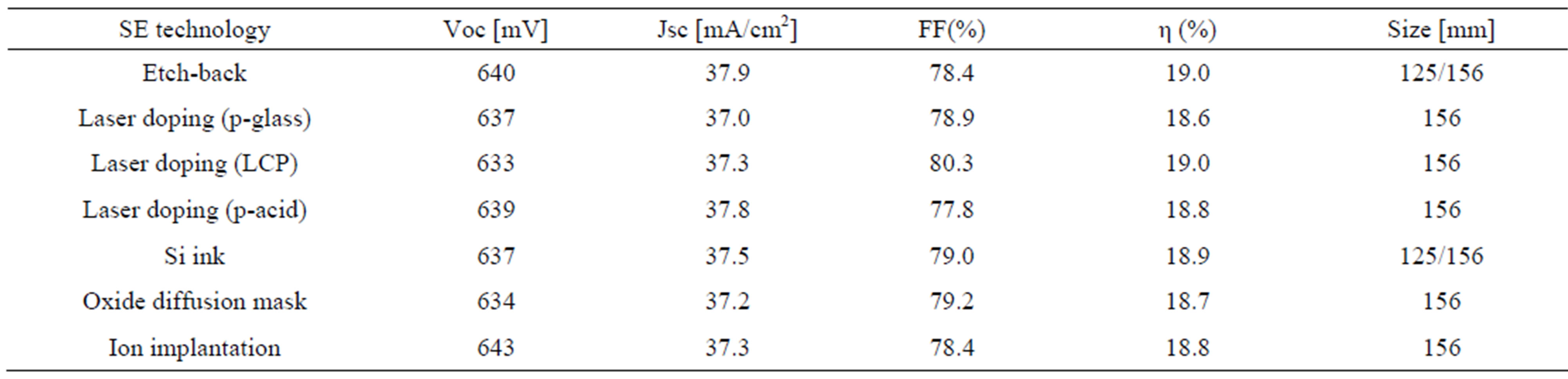
Table 1. I-V results for SE technologies (B-doped Cz, full Al-BSF). Given is best cell I-V parameters [after ref. 3].
SiNx: H layer with a higher refractive index increases implied VOC values even further. The full benefit of the improved front side in terms of a selective emitter structure will be achieved when local rear contacts are used.
However, whenever a particular process is required to be optimized, the amount of extra steps should be kept to an absolute minimum and ideally the general cell line concept should not be changed drastically to make the approach cost-effective and easy to implement.
6. Acknowledgements
My sincere thanks go to Dr. A. R. Mollah for giving me the opportunity to write this article here at AUST.
REFERENCES
- J. Bultman, I. Cesar, B. Geerlings, Y. Komatsu and W. Sinke, “Methods of Emitter Formation for Crystalline Silicon Solar Cells,” Photovoltaics International, Petten, 2010.
- Y. Komatsu, et al., “Innovative Diffusion Processes for Improved Efficiency on Industrial Solar Cells by Doping Profile Manipulation,” Proceedings of the 24th European Photovoltaic Solar Energy Conference and Exhibition, Hamburg, 21-25 September 2009, pp. 1063-1067.
- G. Hahn, “Status of Selective Emitter Technologies,” 25th European Photovoltaic Solar Energy Conference and Exhibition/5th World Conference on Photovoltaic Energy Conversion, Valencia, 6-10 September 2010, pp. 1091-1096.
- A. Ebong, A. Rohatgi, W. Zhang and M. Neidert, “Understanding the Role of Glass Frit in the Front Ag Paste for High Sheet Resistance Emitters,” Proceedings of the 22nd European Photovoltaic Solar Energy Conference and Exhibition, Milan, 3-7 September 2007, p. 1734.
- M. Hörteis and S. Glunz, “Progress in Photovoltaics: Research and Applications,” Vol. 16, No. 7, 2008, pp. 555- 560. doi:10.1002/pip.850
- F. Book, A. Dastgheib-Shirazi, B. Raabe, H. Haverkampl, G. Hahn and P. Grabitz, “Detailed Analysis of High Sheet Resistance Emitters for Selectively Doped Silicon Solar Cells,” Proceedings of the 24th European Photovoltaic Solar Energy Conference and Exhibition, Hamburg, 21-25 September 2009, pp. 1719-1722.
- B. Raabe, F. Book, A. Dastgheib-Shirazi and G. Hahn, “The Development of Etch-Back Processes for Industrial Silicon Solar Cells,” Proceedings of the 25th European Photovoltaic Solar Energy Conference and Exhibition/5th World Conference on Photovoltaic Energy Conversion, Valencia, 6-10 September 2010, pp. 1174-1178.
- H. Haverkamp, A. Shirazi, B. Raabe, F. Book and G. Hahn, “Minimizing the Electrical Losses on the Front Side: Development a Selective Emitter Process from a Single Diffusion,” The 33rd IEEE Photovoltaic Solar Energy Conference and Exhibition, San Diego, 11-16 May 2008, pp. 430-433.
- T. Lauermann, A. Dastgheib-Shirazi, F. Book, B. Raabe, G. Hahn, H. Haverkamp, D. Habermann, C. Demberger and C. Schmid, “Insect: An Inline Selective Emitter Concept with High Efficiencies at Competitive Process Costs Improved with Inkjet Masking Technology,” The 24th European Photovoltaic Solar Energy Conference and Exhibition, Hamburg, 21-25 September 2009, pp. 1767-1770.
- A. Dastgheib-Shirazi, H. Haverkamp, B. Raabe, F. Book and G. Hahn, “Selective Emitter for Industrial Solar Cell Production: A Wet Chemical Approach Using a Single Side Diffusion Process,” Proceedings of the 23rd European Photovoltaic Solar Energy Conference and Exhibition, Valencia, 1-5 September 2008, pp. 1197-1199.
- T. Lauermann, F. Book, A. Dastgheib-Shirazi, G. Hahn, H. Haverkamp, R. Bleidiessel and M. Fleuster, “The Optimal Choice of the Doping Levels in an Inline Selective Emitter Design for Screen Printed Multicrystalline Silicon Solar Cells,” Proceedings of the 24th European Photovoltaic Solar Energy Conference and Exhibition, Hamburg, 21-25 September 2009, pp.1795-1797.
- J. Werner, J. Kohler and A. Esturo Breton, “A Method of Laser Doping of Solids with a Laser Line Focused,” German Patent No. DE 10 2004 036 220 B 4, 2009.
- P. Engelhart, S. Hermann, T. Neubert, H. Plagwitz, R. Grischke, R. Meyer, U. Klug, A. Schoonderbeek, U. Stute and R. Brendel, “Laser Ablation of SiO2 for Locally Contacted Si Solar Cells with Ultra-Short Pulses,” Progress in Photovoltaics: Research and Applications, Vol. 15, No. 6, 2007, pp. 521-527. doi:10.1002/pip.758
- S. J. Eisele, T. C. Röder, J. R. Köhler and J. H. Werner, “18.9% Efficient Full Area Laser Doped Silicon Solar Cell,” Applied Physics Letters, Vol. 95, No. 13, 2009, pp. 133501-133504. doi:10.1063/1.3232208
- J. Köhler, P. Grabitz, S. Eisele, T. Röder and J. Werner, “Laser Doped Selective Emitters Yield 0.5% Efficiency Gain,” Proceedings of the 24th European Photovoltaic Solar Energy Conference and Exhibition, Hamburg, 21-25 September 2009, pp. 1847-1850.
- D. Kray, N. Bay, G. Cimiotti, S. Kleinschmidt, Kösterke, A. Lösel, M. Sailer, A. Träger, H. Kühnlein, Nussbaumer, C. Fleischmann and F. Granek, “Industrial LCP Selective Emitter Solar Cells with Plated Contacts,” 35th IEEE Photovoltaic Solar Energy Conference and Exhibition, Honolulu, 20-25 June 2010.
- B. Tjahjono, S. Wang, A. Sugianto, L. Mai, Hameiri, N. Borojevic, A. Ho-Baillie and S. R. Wenham, “Application of Laser Doped Contact Structure on Multicrystalline Solar Cells,” Proceedings of the 23rd European Photovoltaic Solar Energy Conference and Exhibition, Valencia, 1-5 September 2008, pp. 1995-2000.
- H. Antoniadis, F. Jiang, W. Shan and Y. Liu, “All Screen Printed Mass Produced Silicon Ink Selective Emitter Solar Cells,” Proceedings of the 35th IEEE Photovoltaic Solar Energy Conference and Exhibition, Honolulu, 20- 25 June 2010.
- A. Esturo-Breton, F. Binaie, M. Breselge, T. Friess, M. Geiger, E. Holbig, J. Isenberg, S. Keller, T. Kühn, J. Maier, A. Münzer, R. Schlosser, A. Schmid, C. Voyer, P. Winter, K. Bayer, J. Krümberg, S. Henze, I. Melnyk, M. Schmidt, S. Klingbeil, F. Walter, R. Kopecek and K. Peter, “Crystalline Si Solar Cells with Selective Emitter for Industrial Mass Production,” Proceedings of the 24th European Photovoltaic Solar Energy Conference and Exhibition, Hamburg, 21-25 September 2009, p. 1068.
- R. Low, A. Gupta, N. Bateman, D. Ramappa, P. Sullivan, W. Skinner, J. Mullin and S. Peters, “High Efficiency Selective Emitter Enabled through Patterned Ion Implantation,” Proceedings of the 35th IEEE Photovoltaic Solar Energy Conference and Exhibition, Honolulu, 20-25 June 2010.
- A. Ebong, I. B. Cooper, B. Rounsaville, K. Tate, A. Rohatgi, B. Bunkenburg, J. Cathey, S. Kim and D. Ruf, “High Efficiency Inline Diffused Emitter (ILDE) Solar Cells on Mono-Crystalline CZ Silicon,” Progress in Photovoltaics: Research and Applications, Vol. 18, No. 8, 2010, pp. 590-595. doi:10.1002/pip.982
- D. S. Kim, B. Rounsaville, A. Pandey, A. Ebong, V. Upadhyaya, A. Upadhyaya, K. Tate, V. Yelundur, A. Rohatgi and J. Simpson, “Low-Cost, High-Throughput Emitter Formation Technologies Using a Ceramic Roller Hearth Metal-Free Diffusion Furnace for Crystalline Silicon Solar Cells,” Proceedings of the 16th Workshop on Crystalline Silicon Solar Cell Material and Process, Vail, 6-9 August 2006.
- M. M. Hilali, M. M. Al-Jassim, B. To, H. Moutinho, A. Rohatgi and S. Asher, “Understanding the Formation and Temperature Dependence of Thick-Film Ag Contacts on High-Sheet-Resistance Si Emitters for Solar Cells,” Journal of the Electrochemical Society, Vol. 152, No. 10, 2005, pp. G742-G749. doi:10.1149/1.2001507