Materials Sciences and Applications
Vol. 3 No. 11 (2012) , Article ID: 24930 , 5 pages DOI:10.4236/msa.2012.311116
Sulphurization of the Electrochemically Deposited Indium Sulphide Oxide Thin Film and Its Photovoltaic Applications
![]()
1Fayoum University, Fayoum, Egypt; 2Tokyo University of Science, Tokyo, Japan; 3Nagoya Institute of Technology, Nagoya, Japan.
Email: *ama05@fayoum.edu.eg
Received August 23rd, 2012; revised September 21st, 2012; accepted October 18th, 2012
Keywords: Indium Sulphide Oxide; Electrochemical Depositon; Thin Films; Sulphurization; Cd-Free Buffer Layer; Solar Cells
ABSTRACT
The post-deposition heat treatment (annealing) for the electrochemically deposited thin film is often necessary in order to improve its crystallinity. In the present study, the electrochemically deposited indium sulfide oxide thin film was annealed in sulphure atmosphere for 60 min at 150˚C and 300˚C. The impact of the annealing process on the composition, crystal structure, and surface morphology of the thin film was investigated. In addition, superstrate heterojunction solar cells based on the annealed film as a buffer layer and tin sulphide as an active layer were fabricated and characterized. They showed diode-like behavior under dark condition and a relatively small photovoltaic effect under AM1.5 illumination condition.
1. Introduction
There is a great interest to replace the cadmium sulphide (CdS) thin film by a cadmium-free wide band gap buffer layer in solar cell applications, for environmental reasons and possible gains in efficiency associated with an increase in the short circuit current. Indium-based thin film buffers are good candidates, and thus they have been successfully synthesized by numerous techniques [1-10]. Thin films based on indium sulphide have been already utilized as Cd-free buffer layers for solar cell applications [11-16].
In previous reports we deposited indium sulphide oxide (InSxOy) thin films using the electrochemical deposition technique (ECD) [17,18]. The as-deposited films were amorphous in nature and included elemental indium in a polycrystalline structure. In order to improve their crystalline structure, the deposited films were annealed in nitrogen atmosphere at 100˚C, 200˚C, 300˚C and 400˚C [19]. Phase transition happened only at 400˚C and the structure of the 400˚C-annelaed film was polycrystalline. Due to annealing at such relatively high temperature (400˚C), almost all the sulphure content escaped from the film and oxygen, from the atmosphere, partly replaced it. This might be inversely affected the electrical properties of the annealed films.
In the present study, the deposited films were annealed in sulphure atmosphere (sulphurization) in order to improve their structure without sulphure deficiency; escaped sulphure is compensated from the atmosphere. Additionally, solar cells were fabricated using the sulphurized InSxOy thin films as buffer layers and tin sulphide (SnS) thin films as absorber layers. SnS thin film was chosen due to its promising advantages as an absorber layer for solar cell applications. SnS is a p-type semiconductor that possesses a band gap of 1.1 - 1.5 eV that is close to the optimum value required for efficient light absorption [20]. In addition, its constituent elements, Sn and S are non-toxic and abundant in earth crust. Moreover, SnS can be easily deposited even using simple techniques such as chemical bath deposition [21,22], and ECD [23-25].
2. Experimental Methods
2.1. Films Deposition and Annealing
The InSxOy thin films were deposited onto glass substrate coated with fluorine doped tin oxide (FTO) thin film. The films were deposited by the ECD technique from an aqueous bath that contained 10 mM of In2(SO4)3 and 100 mM of Na2S2O3 at room temperature without intentional adjustment of the pH value (pH ~ 2.5) of the bath. The power supply of the ECD apparatus was adjusted to generate voltage in the two-step periodic-pulse form, The first voltage-step equal to –1.15 V and the second one equal to –0.4 V and the time-interval of each pulse equal to 10 sec. The deposited film was ~0.2 μm in thickness. More details about the deposition apparatus and conditions are mentioned elsewhere [17,26]. A post-deposition heat treatment was performed for the deposited films in sulphure atmosphere for 60 min at two different temperatures, namely 150˚C and 300˚C.
The structural, compositional, and optical properties of the as-deposited as well as the annealed films were characterized by various techniques. The structure of the films was studied using the desktop X-ray diffractometer (Rigaku, MiniFlex II). The compositional analysis was carried out by energy dispersive X-ray spectroscope (EDX; Hitachi Miniscope TM-1000) keeping the acceleration voltage at 15 kV and Auger electron spectroscopy (AES) using the model JEOL JAMP 7800 Auger microprobe at probe voltage 10 kV and current 2 × 10⁻⁸ A. In the AES machine an argon-ion sputtering with acceleration voltage 3 kV and current 20 mA was used to sputter the film surface. Based on AES measurements, the S/In and O/In atomic ratios were calculated using standard In2S3 and In2O3 compounds, respectively. The surface morphology of the film was analyzed by scanning electron microscope (SEM; Hitachi Miniscope TM-1000), keeping the acceleration voltage at 15 kV and magnification at 10,000.
Finally, the chemical bonds among the constituent elements were investigated by the X-ray photoelectron spectroscope (XPS, PHI 5000 VersaProbe). Sputtering was accomplished at 3 mA emission current and a 3 kV beam energy using an Argon ion gun at vacuum pressure equal to 1.1 × 10⁻⁷ Torr.
2.2. Solar Cell Fabrication
The solar cell was fabricated in the form of superstrate heterjunction configuration. A 0.8-μm-thick SnS thin film was electrochemically deposited onto the annealed InSxOy thin film and then the indium metal electrodes were deposited as back contacts by thermal evaporation. Thus the structure of the fabricated solar cell could be represented by [glass/FTO/InSxOy/SnS/In] form. The SnS thin film was deposited from an aqueous bath that contained SnSO4 (25 mM) and Na2S2O3 (100 mM). The pH value of the bath was not intentionally adjusted (pH = 3). A three-step pulse voltage was applied to the substrate, V1 = 0, V2 = –0.6, and V3 = –1.0 V vs SCE, they are applied for 10, 10, and 6 sec, respectively [25]. The size of each indium electrode is 1 mm2 and the distance between two adjacent electrodes is 1 mm.
3. Results and Discussions
Figures 1(a) and (b) showed the SEM measurements of
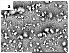
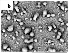
Figure 1. SEM measurements that show the surface morphology of films annealed at 150˚C (a) and 300˚C (b).
films annealed at 150˚C and 300˚C, respectively. The figures revealed that films cover the substrate without cracks or voids. It is noticeable that the white particles distributed at the film surface became little bigger after annealing at 300˚C.
Figures 2(a) and (b) showed the energy dispersive X-ray spectroscopy (EDX) measurements that were performed at the white particles distributed at the surface of the as-deposited and 300˚C-annealed InSxOy thin films, respectively. Figure 2(a) revealed that the white particles are very indium-rich. However, those white particles became sulphure-rich for the film annealed at 300˚C, as shown in Figure 2(b). This means that the excess indiumatoms of the white particles were sulphurized due to annealing at 300˚C.
A quantitative study, shown in Table 1, of the film composition was performed based on the Auger electron spectra taken at the flat part of the film surface not at white particles. The spectra were taken after 20 sec of argon-ion etching to remove the contamination that may present at the film surface. The study revealed that annealing at 150˚C slightly increased the sulphure content of the film. However, annealing at 300˚C significantly changed the film composition. The sulphure content obviously increased and the oxygen content almost disappeared as clearly shown in Figure 3. During annealing at such high temperature, 300˚C, oxygen was replaced by sulphure; the oxygen contained in the bulk of the film recombined with the hydrogen presented in the atmosphere to produce the water vapor. However, the [S/In] ratio of the 300˚C-annealed film was 2.2 instead 1.5 as of β-In2S3 thin film. This means that the film consisted of β-In2S3 and another secondary InxSy phase. The XRD measurements confirmed only the presence of the β-In2S3. This means that the secondary phase may present in the amorphous or nanocrystalline structure.
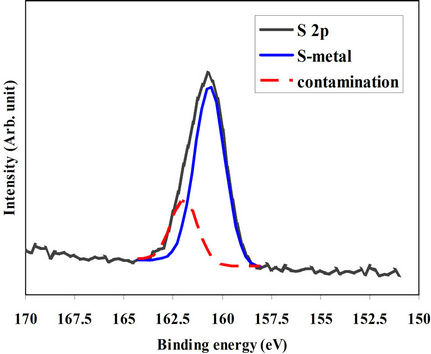
The XPS spectrum of S 2p energy level of the 300˚Cannealed film was measured at the film surface and after different time intervals of sputtering. Figures 4(a) and (b) showed the spectra of S 2p measured at the surface and after 30 sec of sputtering of the 300˚C-annealed film, respectively. The peak of the spectrum taken at the surface could be represented by two separate peaks. The
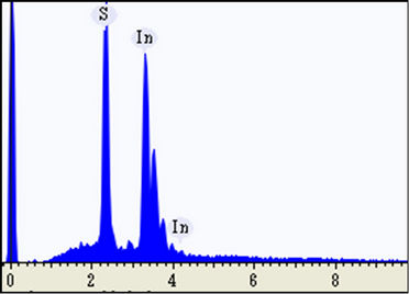
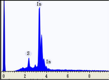
Figure 2. EDX measurement taken at one of the white particles distributed over the surface of the as-deposited (a) and 300˚C-annealed (b) thin films.
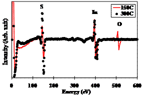
Figure 3. AES spectra of the films annealed at 150 and 300˚C after 20 sec of Argon-ion sputtering.
major peak belongs to the sulphure-to-indium pond and the minor one refers to the sulphure contamination (oxidized sulphure). After 30 sec of sputtering the contamination peak completely disappeared and the only remained peak is that of S-In pond. 300˚C-annealed films are bonded only to indium atoms and the contamination layer is tiny and superficial.
Concerning the crystal structure of the film, we confirmed in the previous report that the as-deposited InSxOy thin film was amorphous in nature and contained polycrystalline indium metal in its bulk [18]. However, phase transition happened after annealing at 400˚C in nitrogen atmosphere; polycrystalline β-In2S3 phase is formed in
 (a)
(a)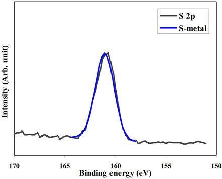 (b)
(b)
Figure 4. (a) XPS spectrum of S 2p energy level taken at the surface (a) and after 30 sec of Argon-ion sputtering (b) of the film annealed at 300˚C.
the bulk of the film and the indium metal was totally disappeared. The XRD spectra of films annealed at 150 and 300˚C in sulphure atmosphere are shown in Figure 5. The figure revealed that the film became polycrystalline β-In2S3 due to annealing at 300˚C. This means that the presence of sulphure in the atmosphere, instead of nitrogen, during the annealing process resulted in phase transition at 300˚C instead of 400˚C and thus a considerable amount of energy could be conserved.
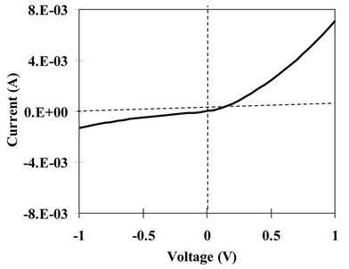
The indium sulfide oxide thin film annealed at 300˚C was incorporated in a SnS-based heterojunction solar cell [glass/FTO/InSxOy/SnS/In]. Figures 6(a) and (b) showed the I-V characteristics under dark and illumination (AM1.5) conditions, respectively. The figures revealed that the solar cell has a rectification property (diode-like behavior) and a noticeable photovoltaic effect. Nevertheless, the photovoltaic conversion efficiency of this solar cell is still very low and it needs more improvement. The reason behind the poor efficiency is not clear, however,
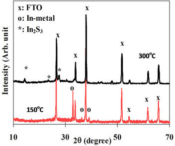
Figure 5. XRD spectra of films annealed at 150˚C and 300˚C.
 (a)
(a)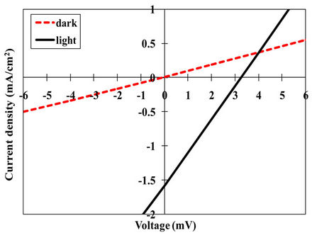 (b)
(b)
Figure 6. I-V characteristic of the [Glass/FTO/300˚C-annealed InSxOy/SnS/In] solar cells under dark (a) and illumination (b) conditions (solid line); dashed line is under dark.
it may be due to the relatively large grains at the surface of the bottom layer (InSxOy) that inversely affect the electrical properties at the interface.
4. Conclusions
The electrochemically deposited InSxOy thin films were annealed in sulphure atmosphere at 150˚C and 300˚C for 60 minutes. The properties; namely composition, crystal structure, and surface morphology of the annealed films were studied. Annealing at 150˚C did not introduce a noticeable modification to those properties. However, annealing at 300˚C resulted in a considerable modification for the film properties. Sulphure content was increased in the film bulk replacing oxygen. The structure of the film became polycrystalline instead of amorphous. Moreover, XRD peaks of the indium metal were completely disappeared; excess indium-atoms might be get sulphurized to form β-In2S3. The surface morphology of the film annealed at 300˚C is almost similar to that of the film annealed at 150˚C except the white particles distributed at the surface of the 300˚C-annealed film are little bigger. The EDX measurements revealed that the white particles distributed at the film surface are in-rich particles that get sulphurized due to annealing at 300˚C. The XPS measurements revealed that the sulphure atoms incorporated in the bulk of the film are bonded to indium atoms.
The [glass/FTO/InSxOy/SnS/In] heterojunction solar cell showed diode-like behavior and photovoltaic effect. However, the conversion efficiency still very low and needs further improvement.
5. Acknowledgements
We would like to thank Dr. M. Kato for his useful discussions.
REFERENCES
- S. Gall, N. Barreau, S. Harel, J. C. Bernede and J. Kessler, “Material Analysis of PVD-Grown Indium Sulphide Buffer Layers for Cu(In,Ga)Se2-Based Solar Cells,” Thin Solid Films, Vol. 480-481, 2005, pp. 138-141. doi:10.1016/j.tsf.2004.11.017
- D. Abou-Ras, G. Kostorz, D. Hariskos, R. Menner, M. Powalla, S. Schorr and A. N. Tiwari, “Structural and Chemical Analyses of Sputtered InxSy Buffer Layers in Cu(In,Ga)Se2 Thin-Film Solar Cells,” Thin Solid Films, Vol. 517, No. 8, 2009, pp. 2792-2798. doi:10.1016/j.tsf.2008.10.138
- S. Spiering, L. Bürkert, D. Hariskos, M. Powalla, B. Dimmler, C. Giesen and M. Heuken, “MOCVD Indium Sulphide for Application as a Buffer Layer in CIGS Solar Cells,” Thin Solid Films, Vol. 517, No. 7, 2009, pp. 2328- 2331. doi:10.1016/j.tsf.2008.11.004
- S. Spiering, A. Eicke, D. Hariskos, M. Powalla, N. Naghavi and D. Lincot, “Large-Area Cd-Free CIGS Solar Modules with In2S3 Buffer Layer Deposited by ALCVD,” Thin Solid Films, Vol. 451-452, 2004, pp. 562-566. doi:10.1016/j.tsf.2003.10.090
- T. Asikainen, M. Ritala and M. Leskelä, “Growth of In2S3 Thin Films by Atomic Layer Epitaxy,” Applied Surface Science, Vol. 82-83, 1994, pp. 122-125. doi:10.1016/0169-4332(94)90206-2
- N. A. Allsop, A. Schönmann, A. Belaidi, H.-J. Muffler, B. Mertesacker, W. Bohne, E. Strub, J. Röhrich, M. C. LuxSteiner and Ch.-H. Fischer, “Indium Sulfide Thin Films Deposited by the Spray Ion Layer Gas Reaction Technique,” Thin Solid Films, Vol. 513, No. 1-2, 2006, pp. 52- 56. doi:10.1016/j.tsf.2006.01.019
- K. Ernits, D. Brémaud, S. Buecheler, C. J. Hibberd, M. Kaelin, G. Khrypunov, U. Müller, E. Mellikov and A. N. Tiwari, “Characterisation of Ultrasonically Sprayed InxSy Buffer Layers for Cu(In,Ga)Se2 Solar Cells,” Thin Solid Films, Vol. 515, No. 15, 2007, pp. 605-6054. doi:10.1016/j.tsf.2006.12.168
- M. T. Herrero, C. Gutierrez, J. M. Guillen, M. A. Dona, A. M. Martinez, R. Chaparro and R. Bayon, “Photovoltaic Windows by Chemical Bath Deposition,” Thin Solid Films, Vol. 361-362, 2000, pp. 28-33. doi:10.1016/S0040-6090(99)00830-5
- J. F. Trigo, B. Asenjo, J. Herrero and M. T. Gutierrez, “Optical Characterization of In2S3 Solar Cell Buffer Layers Grown by Chemical Bath and Physical Vapor Deposition,” Solar Energy Materials and Solar Cells, Vol. 92, No. 9, 2008, pp. 1145-1148. doi:10.1016/j.solmat.2008.04.002
- T. Todorov, J. Carda, P. Escribano, A. Grimm, J. Klaer and R. Klenk, “Electro Deposited In2S3 Buffer Layers for CuInS2 Solar Cells,” Solar Energy Materials and Solar Cells, Vol. 92, No. 10, 2008, pp. 1274-1278. doi:10.1016/j.solmat.2008.04.022
- E. B. Yousfi, T. Asikainen, V. Pietu, P. Cowache, M. Powalla and D. Lincot, “Cadmium-Free Buffer Layers Deposited by Atomic Later Epitaxy for Copper Indium Diselenide Solar Cells,” Thin Solid Films, Vol. 361-362, 2000, pp. 183-186. doi:10.1016/S0040-6090(99)00860-3
- D. Braunger, D. Hariskos, T. Walter and H. W. Schock, “An 11.4% Efficient Polycrystalline Thin Film Solar Cell Based on CuInS2 with a Cd-Free Buffer Layer,” Solar Energy Materials and Solar Cells, Vol. 40, No. 2, 1996, pp. 97-102. doi:10.1016/0927-0248(95)00069-0
- S. Spiering, D. Hariskos, M. Powalla, N. Naghavi and D. Lincot, “CD-Free Cu(In,Ga)Se2 Thin-Film Solar Modules with In2S3 Buffer Layer by ALCVD,” Thin Solid Films, Vol. 431-432, 2003, pp. 359-363. doi:10.1016/S0040-6090(03)00151-2
- E. B. Yousfi, B. Weinberger, F. Donsanti, P. Cowache and D. Lincot, “Atomic Layer Deposition of Zinc Oxide and Indium Sulfide Layers for Cu(In,Ga)Se2 Thin-Film Solar Cells,” Thin Solid Films, Vol. 387, No. 1-2, 2001, pp. 29-32. doi:10.1016/S0040-6090(00)01838-1
- D. Hariskos, M. Ruckh, U. Ruhle, T. Walter, H. W. Schock, J. Hedstrom and L. Stolt, “A Novel Cadmium Free Buffer Layer for Cu(In,Ga)Se2 Based Solar Cells,” Solar Energy Materials and Solar Cells, Vol. 41-42, 1996, pp. 345-353. doi:10.1016/0927-0248(96)80009-2
- H. W. Schock, “Solar Cells Based on CuInSe2 and Related Compounds: Recent Progress in Europe,” Solar Energy Materials and Solar Cells, Vol. 34, No. 1-4, 1994, pp. 19-26. doi:10.1016/0927-0248(94)90020-5
- A. M. A. Haleem and M. Ichimura, “Wide Bandgap InSBased Thin Film: Deposition Characterization and Application in SnS Solar Cells,” Japanese Journal of Applied Physics, Vol. 48, 2009, Article ID: 035506. doi:10.1143/JJAP.48.035506
- A. M. A. Haleem and M. Ichimura, “Electrochemical Deposition of Indium Sulfide Thin Films Using Two-Step Pulse Biasing,” Thin Solid Films, Vol. 516, No. 21, 2008, pp. 7783-7789. doi:10.1016/j.tsf.2008.03.009
- A. M. A. Haleem, M. Kato and M. Ichimura, “Annealing Study of the Electrochemically Deposited InSxOy Thin Film and Its Photovoltaic Application,” IEICE Transactions on Electronics, Vol. E92-C, No. 12, 2009, pp. 1464- 1469.
- A. Goetzberger and C. Hebling, “Photovoltaic Materials, Past, Present, Future,” Solar Energy Materials and Solar Cells, Vol. 62, No. 1-2, 2000, pp. 1-19. doi:10.1016/S0927-0248(99)00131-2
- M. T. S. Nair and P. K. Nair, “Simplified Chemical Deposition Technique for Good Quality SnS Thin Films,” Semiconductor Science and Technology, Vol. 6, 1991, p. 132.
- A. Tanusevski, “Optical and Photoelectric Properties of SnS Thin Films Prepared by Chemical Bath Deposition,” Semiconductor Science and Technology, Vol. 18, 2003, p. 501. doi:10.1088/0268-1242/18/6/318
- Z. Zainal, M. Z. Hussein and A. Ghazali, “Cathodic Electrodeposition of SnS Thin Films from Aqueous Solution,” Solar Energy Materials and Solar Cells, Vol. 40, No. 4, 1996, pp. 347-357. doi:10.1016/0927-0248(95)00157-3
- N. Sato, M. Ichimura, E. Arai and Y. Yamazaki, “Characterization of Electrical Properties and Photosensitivity of SnS Thin Films Prepared by the Electrochemical Deposition Method,” Solar Energy Materials and Solar Cells, Vol. 85, No. 2, 2005, pp. 153-165. doi:10.1016/j.solmat.2004.04.014
- K. Omoto, N. Fathy and M. Ichimura, “Deposition of SnSxOy Films by Electrochemical Deposition Using ThreeStep Pulse and Their Characterization,” Japanese Journal of Applied Physics, Vol. 45, 2006, pp. 1500-1505. doi:10.1143/JJAP.45.1500
- A. M. A. Haleem and M. Ichimura, “Electrochemical Deposition of Wide Bandgap InGaxSyOz Thin Films for Solar Cell Applications,” Materials Science and Engineering B, Vol. 164, No. 3, 2009, pp. 180-185. doi:10.1016/j.mseb.2009.09.013
NOTES
*Corresponding author.