Circuits and Systems
Vol. 3 No. 4 (2012) , Article ID: 23645 , 6 pages DOI:10.4236/cs.2012.34048
Grounded and Floating Inductance Simulation Circuits Using VDTAs
Department of Electronics and Communication Engineering, Faculty of Engineering and Technology, Jamia Millia Islamia, New Delhi, India
Email: *dprasad@jmi.ac.in, dbhaskar@jmi.ac.in
Received August 14, 2012; revised September 10, 2012; accepted September 17, 2012
Keywords: VDTA; Inductance Simulation; Filters
ABSTRACT
New electronically-controllable lossless grounded and floating inductance simulation circuits have been proposed employing Voltage Differencing Transconductance Amplifiers (VDTA). The proposed grounded inductance (GI) circuit employs a single VDTA and one grounded capacitor whereas the floating inductance (FI) circuit employs two VDTAs and one grounded capacitor. The workability of the new circuits has been verified using SPICE simulation with TSMC CMOS 0.18 μm process parameters.
1. Introduction
Several circuits and techniques for the simulation of grounded and floating inductance employing different active elements such as operational amplifiers, current conveyors, current controlled conveyors, current feedback operational amplifiers, operational mirrored amplifiers, differential voltage current conveyors, current differencing buffered amplifiers, current differencing transconductance amplifiers, operational transconductance amplifiers (OTAs) have been reported in the literature see [1-33] and the references cited therein. Many active elements have been introduced by Biolek, Senani, Biolkova and Kolka in [34], VDTA is one of them. A CMOS realization of VDTA and its filter application have also been reported in [35]. The purpose of this paper is, to propose new electronically-controllable VDTAbased lossless GI and FI circuits employing a grounded capacitor. The GI uses only one VDTA along with a grounded capacitor and does not require any matching condition whereas FI employs two VDTAs, a grounded capacitor and requires matching conditions. The workability of the proposed new circuits has been verified using SPICE simulation with TSMC CMOS 0.18 μm process parameters.
2. The Proposed New Configurations
The symbolic notation of the VDTA is shown in Figure 1, where VP and VN are input terminals and Z, X+ and X– are output terminals. All terminals of VDTA exhibit high impedance values [35]. The VDTA can be described by the following set of equations:
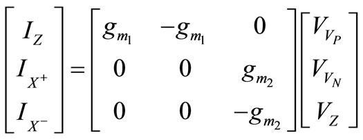 (1)
(1)
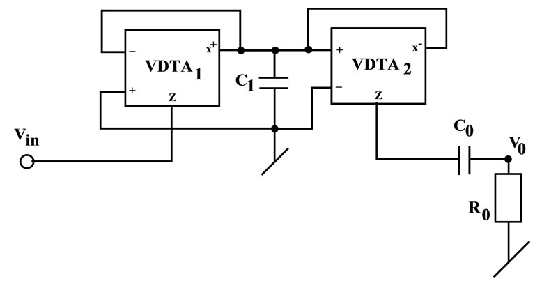
The proposed grounded and floating inductance circuits are shown in Figures 2 and 3 respectively.
A routine circuit analysis of the circuit shown in Figure 2 results in the following expression for the input impedance
 (2)
(2)
The circuit, thus, simulates a grounded inductance with the inductance value given by
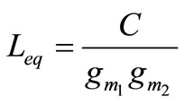 (3)
(3)
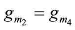
which is electronically controllable by either  or
or .
.
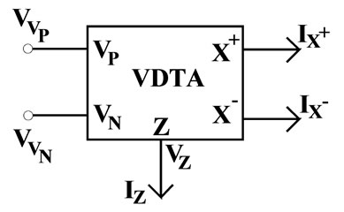
Figure 1. The symbolic notation of VDTA.
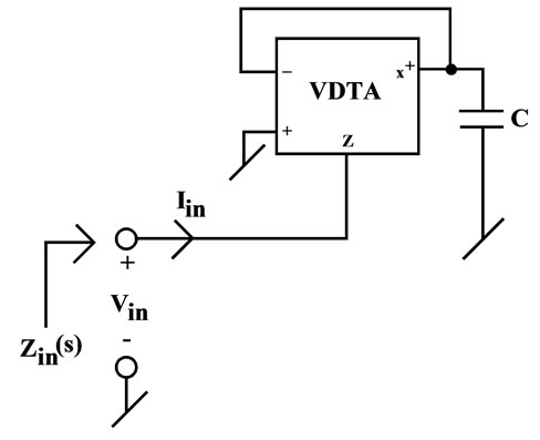
Figure 2. Proposed grounded inductance simulation configuration.
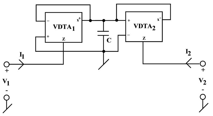
Figure 3. Proposed floating inductance simulation configuration.
On the other hand, analysis of the new FI circuit shown in Figure 3 yields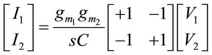 with
with 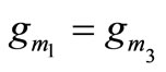 and
and
 (4)
(4)
which proves that the circuit simulates a floating lossless electronically-controllable inductance with the inductance value given by
 (5)
(5)
3. Non-Ideal Analysis and Sensitivity Performance
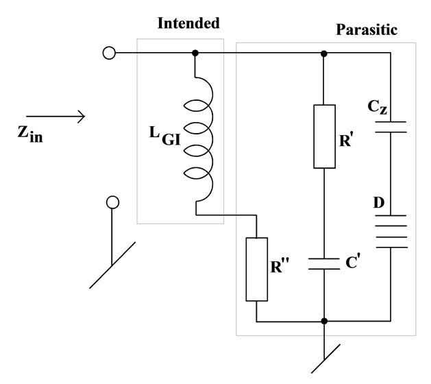
Considering the various VDTA non-ideal parasitics i.e., the finite X-terminal parasitic impedance consisting of a resistance  in parallel with capacitance
  and the parasitic impedance at the Z-terminal consisting of a resistance
  in parallel with capacitance
 .
.
The non-ideal input impedance for the circuit shown in Figure 2 is given by
 (6)
(6)
From Equation (6) a non-ideal equivalent circuit of the grounded inductor is derivable which is shown in Figure 4.
Where ,
,  ,
, 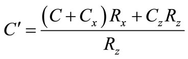 ,
,  and
and 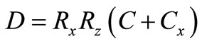
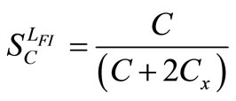
From the above, the sensitivities of LGI with respect to various active and passive elements are found to be
 ,
,  ,
, 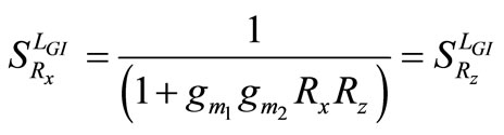 ,
, (7)
(7)
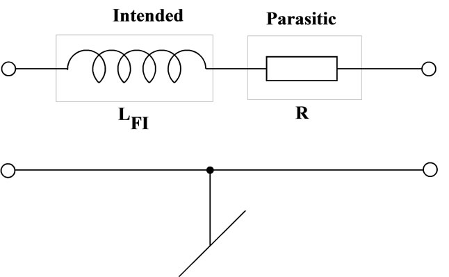
Similarly, for the circuit shown in Figure 3, the input-output current and voltage relationships are given by:
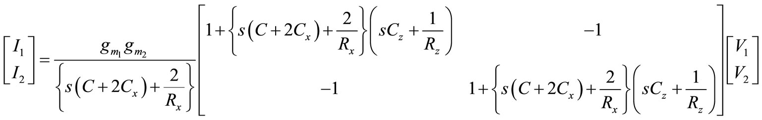
with
 and
and 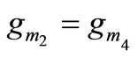 (8)
(8)
The non-ideal equivalent circuit of floating inductor of Figure 3 is derivable from Equation (8) and is shown in Figure 5.
where  and
and 
The various sensitivities of LFI with respect to active and passive elements are:
 ,
,  ,
,
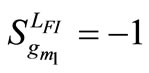 ,
, (9)
(9)
Taking gm1 = gm2 = 631.702 μA/V, Cz = CZ = 0, Rx = Rz = ∞ and C = 0.01nF, these sensitivities are found to be (1, 0, 0, 0, 1, 1) and (1, 0, –1, –1) for Equations (7) and (9) respectively. Thus, all the passive and active sensitivities of both grounded and floating inductance circuits are low.
4. Simulation Results of the New Proposed Grounded/Floating Inductance Configurations
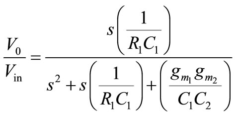
The workability of the proposed simulated inductors has been verified by realizing a band pass filter (BPF) as shown in Figures 6 and 7.
The transfer function realized by this configuration is given by
 (10)
(10)
from where it is seen that bandwidth and centre frequency both are independently tunable, the former by R1 and the latter by any of the transconductances gm1, gm2 and C2.
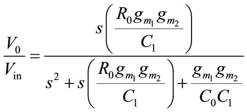
The transfer function realized by the configuration shown in Figure 7 is given by
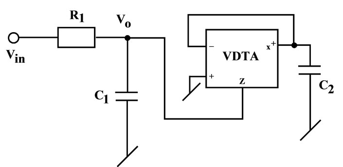
Figure 6. Band pass filter realized by the new grounded simulated inductor.
 with
with 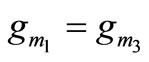
and
 (11)
(11)
In this case, bandwidth is tunable by R0 whereas centre frequency can be tuned by C0.
Performance of the new simulated inductors was verified by SPICE simulations. CMOS-based VDTA from [35] was used to determine the frequency responses of the grounded and floating simulated inductors. The following values were used for grounded as well as floating inductor: C = 0.01 nF, gm1 = gm2 = 631.7 μA/V. From the frequency response of the simulated grounded inductor (Figure 8) it has been observed that the inductance value remains constant upto 10 MHz. Similarly, from the frequency response of the simulated floating inductor (Figure 9) the inductance value also remains constant up to 10 MHz.
To verify the theoretical analysis of the application circuits shown in Figures 6 and 7, these configurations have also been simulated using CMOS VDTAs. The component values used were for Figure 6: C1 = 5 pF, C2 = 0.01 nF, R1 = 1.58 kΩ and for Figure 7: C0 = 0.01 nF, C1 = 5 pF, R0 = 1.58 kΩ. The VDTAs were biased with ±0.9 volts D.C. power supplies with IB1 = IB2 = IB3 = IB4 = 150 μA. Figures 10 and 11 show the simulated filter responses of the BP filters. A comparison of the other

Figure 8. Frequency response of the simulated grounded inductor.

Figure 9. Frequency response of the simulated floating inductor.
previously known grounded and floating inductance simulators has been presented in Table 1.

Figure 10. Frequency response of BPF using the proposed simulated GI.

Figure 11. Frequency response of BPF using the proposed simulated FI.
Table 1. Comparison with other previously known grounded and floating simulators.
The above results, thus, confirm the validity of the applications of the proposed grounded and floating simulated inductance circuits.
5. Conclusion
New electronically-controllable circuits of lossless grounded and floating inductance have been proposed employing VDTAs. The proposed grounded inductance circuit employs only one VDTA and one grounded capacitor. On the other hand, the floating inductance configuration uses two VDTAs and one grounded capacitor, requires realization conditions for floatation. A comparison of the other previously known grounded and floating inductance simulators has been presented in Table 1. The SPICE simulation results have confirmed the workability of the new proposed circuits.
REFERENCES
- R. Senani, “New Single-Capacitor Simulations of Floating Inductors,” ElectroComponent Science and Technology, Vol. 10, No. 1, 1982, pp. 7-10. doi:10.1155/APEC.10.7
- A. Antoniou, “Gyrators Using Operational Amplifiers,” Electronics Letters, Vol. 3, No. 8, 1967, pp. 350-352. doi:10.1049/el:19670270
- A. Antoniou, “Realization of Gyrators Using Op-Amps and Their Use in RC Active Network Synthesis,” Proceedings of the IEEE, Vol. 116, 1969, pp. 1838-1850.
- R. Senani, “Realization of Single Resistance-Controlled Lossless Floating Inductance,” Electronics Letters, Vol. 14, No. 25, 1978, pp. 828-829. doi:10.1049/el:19780560
- R. Senani, “New Tunable Synthetic Floating Inductors,” Electronics Letters, Vol. 16, No. 10, 1980, pp. 382-383. doi:10.1049/el:19800270
- T. S. Rathore and B. M. Singhi, “Active RC Synthesis of Floating Immittances,” International Journal of Circuit Theory and Applications, Vol. 8, No. 2, 1980, pp. 184- 188. doi:10.1002/cta.4490080212
- R. Nandi, “Lossless Inductor Simulation: Novel Configurations Using DVCCs,” Electronics Letters, Vol. 16, No. 17, 1980, pp. 666-667. doi:10.1049/el:19800472
- R. Senani, “Some New Synthetic Floating Inductance Circuits,” International Journal of Electronic and Communications, Vol. 35, 1981, pp. 307-310.
- R. Senani, “Canonic Synthetic Floating-Inductance Circuits Employing Only a Single Component-Matching Condition,” Journal of IETE, Vol. 27, No. 6, 1981, pp. 201-204.
- K. Pal, “Novel Floating Inductance Using Current Conveyors,” Electronics Letters, Vol. 17, No. 18, 1981, p. 638. doi:10.1049/el:19810447
- V. Singh, “Active RC Single-Resistance-Controlled Lossless Floating Inductance Simulation Using Single Grounded Capacitor,” Electronics Letters, Vol. 17, No. 24, 1981, pp. 920-921. doi:10.1049/el:19810641
- R. Senani, “Novel Lossless Synthetic Floating Inductor Employing a Grounded Capacitor,” Electronics Letters, Vol. 18, No. 10, 1982, pp. 413-414. doi:10.1049/el:19820283
- R. Senani, “Three Op-Amp Floating Immittance Simulators: A Retrospection,” IEEE Transactions on Circruits and Systems, Vol. 36, No. 11, 1989, pp. 1463-1465. doi:10.1109/31.41305
- A. Fabre, “Gyrator Implementation from Commercially Available Trans Impedance Operational Amplifiers,” Electronics Letters, Vol. 28, No. 3, 1992, pp. 263-264. doi:10.1049/el:19920162
- R. Senani and J. Malhotra, “Minimal Realizations of a Class of Operational Mirrored Amplifier Based Floating Impedance,” Electronics Letters, Vol. 30, No. 14, 1994, pp. 1113-1114. doi:10.1049/el:19940791
- S. A. Al-Walaie and M. A. Alturaigi, “Current Mode Simulation of Lossless Floating Inductance,” International Journal of Electronics, Vol. 83, No. 6, 1997, pp. 825-830. doi:10.1080/002072197135094
- W. Kiranon and P. Pawarangkoon, “Floating Inductance Simulation Based on Current Conveyors,” Electronics Letters, Vol. 33, 1997, pp. 1748-1749. doi:10.1049/el:19971202
- P. V. Anand Mohan, “Grounded Capacitor Based Grounded and Floating Inductance Simulation Using Current Conveyors,” Electronics Letters, Vol. 34, No. 11, 1998, pp. 1037-1038. doi:10.1049/el:19980783
- O. Cicekoglu, “Active Simulation of Grounded Inductors with CCII+s and Grounded Passive Elements,” International Journal of Electronics, Vol. 85, No. 4, 1998, pp. 455-462. doi:10.1080/002072198134003
- M. T. Abuelma’atti, M. H. Khan and H. A. Al-Zaher, “Simulation of Active-Only Floating Inductance,” Journal of RF-Engineering and Telecommunications, Vol. 52, 1998, pp. 161-164.
- H. Sedef and C. Acar, “A New Floating Inductor Circuit Using Differential Voltage Current Conveyors,” Journal of RF-Engineering and Telecommunications, Vol. 54, 2000, pp. 123-125.
- D. Biolek and V. Biolkova, “Tunable Ladder CDTABased Filters,” 4th Multiconference WSEAS, Spain, 2003, pp. 1-3.
- A. U. Keskin and H. Erhan, “CDBA-Based Synthetic Floating Inductance Circuits with Electronic Tuning Properties,” ETRI Journal, Vol. 27, No. 2, 2005, pp. 239- 242. doi:10.4218/etrij.05.0204.0055
- E. Yuce, S. Minaei and O. Cicekoglu, “A Novel Grounded Inductor Realization Using a Minimum Number of Active and Passive Components,” ETRI Journal, Vol. 27, No. 4, 2005, pp. 427-432. doi:10.4218/etrij.05.0104.0149
- W. Tangsrirat and W. Surakampontorn, “Electronically Tunable Floating Inductance Simulation Based on Current-Controlled Current Differencing Buffered Amplifiers,” Thammasat International Journal of Science and Technology, Vol. 11, No. 1, 2006, pp. 60-65.
- E. Yuce, “On the Realization of the Floating Simulators Using Only Grounded Passive Components,” Analog Integrated Circuits and Signal Processing, Vol. 49, 2006, pp. 161-166. doi:10.1007/s10470-006-9351-7
- T. Parveen and M. T. Ahmed, “Simulation of Ideal Grounded Tunable Inductor and Its Application in High Quality Multifunctional Filter,” Microelectronics Journal, Vol. 23, No. 3, 2006, pp. 9-13. doi:10.1108/13565360610680703
- E. Yuce, “Grounded Inductor Simulators with Improved Low Frequency Performances,” IEEE Transactions on Instrumentation and Measurement, Vol. 57, No. 5, 2008, pp. 1079-1084. doi:10.1109/TIM.2007.913822
- K. Pal and M. J. Nigam, “Novel Active Impedances Using Current Conveyors,” Journal of Active and Passive Electronic Devices, Vol. 3, 2008, pp. 29-34.
- D. Prasad, D. R. Bhaskar and A. K. Singh, “New Grounded and Floating Simulated Inductance Circuits using Current Differencing Transconductance Amplifiers,” Radioengineering, Vol. 19, No. 1, 2010, pp. 194- 198.
- D. Biolek and V. Biolkova, “First-Order Voltage-Mode All-Pass Filter Employing One Active Element and One Grounded Capacitor,” Analog Integrated Circuits and Signal Processing, Vol. 65, No. 1, 2010, pp. 123-129. doi:10.1007/s10470-009-9435-2
- D. Prasad, D. R. Bhaskar and K. L. Pushkar, “Realization of New Electronically Controllable Grounded and Floating Simulated Inductance Circuits Using Voltage Differencing Differential Input Buffered Amplifiers,” Active and Passive Electronic Components, Vol. 2011, 2011, Article ID: 101432. doi:10.1155/2011/101432
- R. Senani and D. R. Bhaskar, “New Lossy/Loss-Less Synthetic Floating Inductance Configuration Realized with Only two CFOAs,” Analog Integrated Circuits and Signal Processing, 2012. doi:10.1007/s10470-012-9897-5
- D. Biolek, R. Senani, V. Biolkova and Z. Kolka, “Active Elements for Analog Signal Processing; Classification, Review and New Proposals,” Radioengineering, Vol. 17, No. 4, 2008, pp. 15-32.
- A. Yesil, F. Kacar and H. Kuntman, “New Simple CMOS Realization of Voltage Differencing Transconductance Amplifier and Its RF Filter Application,” Radioengineering, Vol. 20, No. 3, 2011, pp. 632-637.
NOTES
*Corresponding author.