Journal of Modern Physics
Vol.4 No.11(2013), Article ID:40050,3 pages DOI:10.4236/jmp.2013.411183
The Conductivity of Indium Phosphide Irradiated by Fast Electrons
Institute of Physics, Azerbaijan National Academy of Sciences, Baku, Azerbaijan
Email: sh.sh.rashidova@gmail.com
Copyright © 2013 Sh. Sh. Rashidova. This is an open access article distributed under the Creative Commons Attribution License, which permits unrestricted use, distribution, and reproduction in any medium, provided the original work is properly cited.
Received May 27, 2013; revised June 29, 2013; accepted July 24, 2013
Keywords: Antistructural Defects; Activation Energy; Indium Phosphide; Radiothermoluminescence Method
ABSTRACT
In this work, studied electrical conductivity(s) and annealing of radiation defects in crystals of n-InP are irradiated by electrons energy of 6 MeV and doses of 1017 el/cm2 (centimeter) and 2 × 10¹⁷ el/cm2 (centimeter). It is shown that alongside point defects (in the form of complexes with impurity atoms in crystals of n-InP) also form the complex defects of the type of disordered areas, annealing of which proceeds at T > 300˚C that binds accumulating radiation defects.
1. Introduction
Investigations of the effects of fast electrons irradiation on the electrical properties of InP are of scientific and practical interest. From the scientific point of view, such investigations give information about the origin of radiation—induced defects in InP. From the practical viewpoint, it should note the technology of fabrication of transistors, solar elements and solar cells on InP.
The introduction of high-energy ions in the crystal impurities is accompanied by disordering of the crystal lattice. For elimination of radiation defects and electrical activation impurities, annealing crystals were applied.
2. Experimental Procedure
Results of researches of electric conductivity of irradiated by electrons 6 MeV with concentrations of n = 1018 cm−3 crystals of n-InP. Irradiation was performed on a linear accelerator type EBA-6 MeV (EBA-Electron beam acceleration). Accelerator worked at a frequency of 50 Hz in the impulsive mode.
Pulse duration equal to 2.5 ISS. The samples had thickness 1000 - 2000 mkm (micrometer). Samples of single crystals of n-InP were obtained by Czochralski method. Irradiation was performed at room temperature. Carry out measurement of electric conductivity(s) before and after irradiation in the temperature range from 80 K to 300 K.
Afterwards, the samples underwent isochronal annealing (heating time 10 min.) in the temperature range from 50˚C to 480˚C.
3. Results and Their Discussion
In Figure 1, it is shown that the temperature dependence of the conductivity in InP crystals with concentration n = 1018 cm−3 before (curve 1) and after electrons irradiation E = 6 MeV, doses D = 1017 el/cm2 (curve 2) and D = 2 × 10¹⁷ el/cm2 (curve 3).
As can be seen from the temperature dependence of the electrical conductivity of crystals in n-InP irradiated by fast electrons with a high dose of conductivity reaches a minimum of about T = 170 K. Decrease of the electrical conductivity in the temperature interval from 100 to 170 K cannot determine mobility. This behavior conductivity might be due to the deep-lying levels of radiation entered defects. At higher temperatures (above 170 K) capture of electrons is reduced. The activation energy is estimated by the high temperature of part E = 0.12 eV which is in good agreement with literature data [1].
The electron irradiation by high-energy enters into crystals InP a high number of donors and acceptors of the high degree of their concentration also influence of irradiation formed stable of interstitial phosphorus [2].
As can be seen from figure irradiation dose 1017 el/cm2 (centimeter) conductivity decreases the slope of the curve disappears completely. But on the second stage of irradiation, the dose D = 2 × 10¹⁷ el/cm2 (centimeter) reduce conductivity increases, observed the minimum (curve 3) at a temperature of 170 K - 180 K. This is probably due to the deep-lying levels of radiation defects caused by irradiation [3] which compensates for the electrical conductivity of the crystal. At higher temperatures about 180 K electronic traps are exempt. Activation energy is estimated from the high temperature part (Figure 1 curve 3) E = 0.14 eV, which agrees well with the temperature data [4].
This is confirmed in work [5] a model where the electron irradiation produces M centers in n-InP. These centers are located in two charging status with the activation energy E = 0.09 eV and E = 0.14 eV. These levels have been detected earlier us [6,7] by method RTL in these crystals irradiated with gamma quanta at a temperature of 170 K, 182 K with the activation energies Ea = 0.09 eV and 0.14 eV respectively. Levels with Ea = 0.09 eV lie within 0.1 eV from the edges of the conduction and valence band are associated with the formation of the complex migration of these vacancy in the material with the admixture in the form of a vacancy is impurity. Level with the energy of activation 0.14 eV appeared in the crystal InP
This phenomenon can be associated with the formation of complexes entered defects and interstitial phosphorus atoms IP.
At annihilation of radiation defect also may decrease the nature of the lattice, however, when the concentration of antistructural defects donors type РІn (atoms R nodes sub lattice In) greater concentration of charge carriers in the InP. It can be noted that non-structure defects formed during the irradiation of particles single crystals А3B5 have a more complex structure than those formed during the crystal growth.
These defects can significantly affect the electrical properties of these materials. Figure 2 shows the temperature dependence of the electrical conductivity (σ) for sample InP before and after 6 MeV irradiation with D = 2 × 10¹⁷ el/cm2 and after isochronal annealing in the temperature range from 50˚C to 480˚C.
As is seen from figure 2 after irradiation, the sharp decrease of the electrical conductivity in the beginning (170 K), and then increase with the increase of temperature independence σ (T) (curves 3,4).
The first slope (E = 0.33 eV) corresponds to a deeper level, the second one (E = 0.41) is probably connected with the of conduction due the formation of disordered regions or to conpensation (after irradiation).
The disordered regions in irradiated semiconductors which modulates the energy bands and strongly effects in the temperature dependence of electrical conductivity. It can be assumed that after the irradiation the disordered regions formed in the sample overlap, and this reduce the efficiency of disordered regions are released as the an-
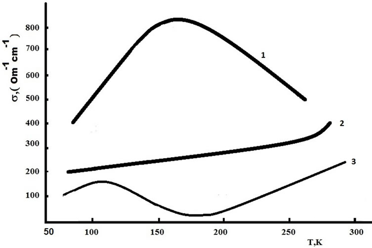
Figure 1. Temperature dependence of the conductivity for crystals n-InP before irradiation; (curve 1) after irradiation with 6 MeV electrons with doses 1017 el/cm2 (curve 2) and 2 × 10¹⁷ el/cm2 (curve 3).
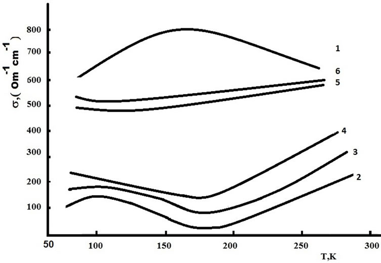
Figure 2. Temperature dependency of the electrical conductivity for sample InP: (1) before irradiation; (2) after irradiation with electron energy E = 6 MeV with dose D = 2 × 10¹⁷ el/cm2 (centimeter); after 10 min isochronal annealing at T = 330˚С (3), 380˚С (4), 430˚С (5), 480˚С (6).
nealing temperature increases.
The isochronal annealing of the irradiated sample gradually recovers the electrical conductivity.
Annealing was performed in quartz ampoules. As is seen from Figure 2 radiation enters the crystal InP a large number of donors and acceptors, also the influence of irradiation is formed stable interstitial atom of phosphorus, the high degree of their compensation. Irradiation is formed by point defects and is stable at room temperature. With the increase of the annealing temperature degree of compensation is reduced.
Deep levels of the created pairs vacancy-antistructural defects (VInInP) the nature belong to defects in crystals with the structure of zinc blende. These deeper levels are within the width of the forbidden zone.
In the presence of crystals of dopants or radiation defects own point defects can form with them complexes.
When ionization defect is a leap nearest phosphorus atom to place vacancies India and complex turns into a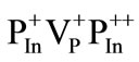 . PIn is antistructural defects of donors’ type.
4. Conclusions
By measuring electrical conductivity, we have found that after irradiation of n-InP crystals with 6 MeV electrons, there arise disordered regions with a space charge, radiation—induced charged defects.
It is also assumed that after electron irradiation, owing to compensation, there appears hopping conduction in InP at T ˂ 170 K, in n-InP to the recharging of the radiation defects available and to the deformation of secondary defects.
Apart from the processes described above, during annealing, secondary defects are formed which would lead to the reverse annealing of conductivity.
REFERENCES
- P. K. Chakraborty and K. P. Ghatak, Journal of Applied Physics, Vol. 89, 2001, pp. 1075-1081. http://dx.doi.org/10.1063/1.1330253
- N. Q. Kolin, D. I. Merkurisov and S. P. Solovyev, FTS, Vol. 34, 2000, in press.
- N. P. Kekelidze, Radiation Effects, 1977, Vol. 32, pp. 113-119. http://dx.doi.org/10.1080/00337577708237465
- J. L. Benton, M. Levinson, A. T. Macrander, H. Tenikin and L. C. Kimerling, Applied Physics Letters, Vol. 45, 1984, p. 566. http://dx.doi.org/10.1063/1.95282
- J. Suski and J. C. Boiurgoins, Journal Applied of Physics, Vol. 54, 1983, p. 2852. http://dx.doi.org/10.1063/1.332277
- Y. W. Zhao, Z. Y. Dong, M. L. Duan and W. R. Sun, European Physical Journal Applied Physics, Vol. 27, 2004, pp. 167-169. http://dx.doi.org/10.1051/epjap:2004096
- Sh. Sh. Rashidova, Journal of Engineering Physics and Thermophysics, Vol. 84, 2011, pp. 479-482. http://dx.doi.org/10.1007/s10891-011-0494-8