Optics and Photonics Journal
Vol.3 No.2(2013), Article ID:32731,6 pages DOI:10.4236/opj.2013.32030
Impact of the Opto-Geometric Parameters on the Band Diagram and Transmission and Reflection Spectrum of the Bragg Structure
Telecommunications and Digital Signal Processing Laboratory, Institute of Electronic,
University Djillali Liabes, Sidi Bel Abbes, Algerie
Email: ouahab_dz@yahoo.fr
Copyright © 2013 Iman Ouahab et al. This is an open access article distributed under the Creative Commons Attribution License, which permits unrestricted use, distribution, and reproduction in any medium, provided the original work is properly cited.
Received March 28, 2012; revise February 17, 2013; accepted February 25, 2013
Keywords: Bragg Structure; PWM; CMM; Graphic User Interface; Photonic Band Gap; Spectrum of Transmission and Reflection
ABSTRACT
Knowledge of the band gap and transmission and reflection spectrum of a photonic crystal is essential elements for their design. A graphical interface that quickly determines the banding pattern and spectrum based on the Plane Wave Method (PWM) and coupled modes method (CMM) respectively is created. It is used to explore the behavior of a Bragg structure with the ability to easily vary the important parameters such as refractive indices, number and thickness of layers.
1. Introduction
Photonic crystals, also known as Photonic Band Gap (PBG) are composed of periodic materials that affect the propagation of electromagnetic waves (EM).
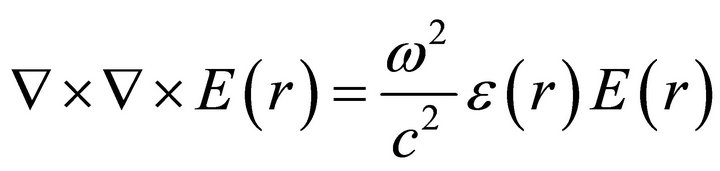
These concepts of photonic band gap structure are derived directly from the numerical solution of Maxwell’s equations in a periodic dielectric medium, and knowing that the periodicity of the crystal potential is the source of energy band gaps in crystals and use of the analogy between electrons and photons resulting from the comparison of the Schrodinger equation and the Maxwell Equations (1) and (2) respectively, the periodicity of the dielectric permittivity (where refractive index) can be exploited in the electromagnetic field [1].
 (1)
(1)
 (2)
(2)
Bragg structure, the simple photonic crystal as one can conceive and realize, formed from multiple layers, resulting in periodic variation in the effective refractive index [2] is widely used in various types of optical devices such as vertical cavity surface-emitting lasers and light-emitting diodes, waveguides, reflectivity modulators, and solar cells [3].
Understanding of such PBG and spectrum of transmission and reflection effects are great importance. To that point, the basic one dimensional photonic crystal is chosen to be investigated for simplicity in this paper.
2. User Interface
Bragg structure is formed from multiple layers resulting in periodic variation in the effective refractive index. Each layer boundary causes a partial reflection of an optical wave. For waves whose wavelength is close to four times the optical thickness of the layers, the many reflections combine with constructive interference, and the layers act as a high-quality reflector. The range of wavelengths that are reflected is called the Photonic Band Gap (stop band) [4].
The simulation is a very helpful tool to study the influence of the different parameters of Bragg structure illustrate in (Figure 1). To facilitate handling programs, a Graphic User Interface (GUI) was created in Matlab. These parameters are:
• Index n1, Index n2: the structure is formed from multiple layers of alternating materials with varying refractive index (n1: High index), (n2: Low index).
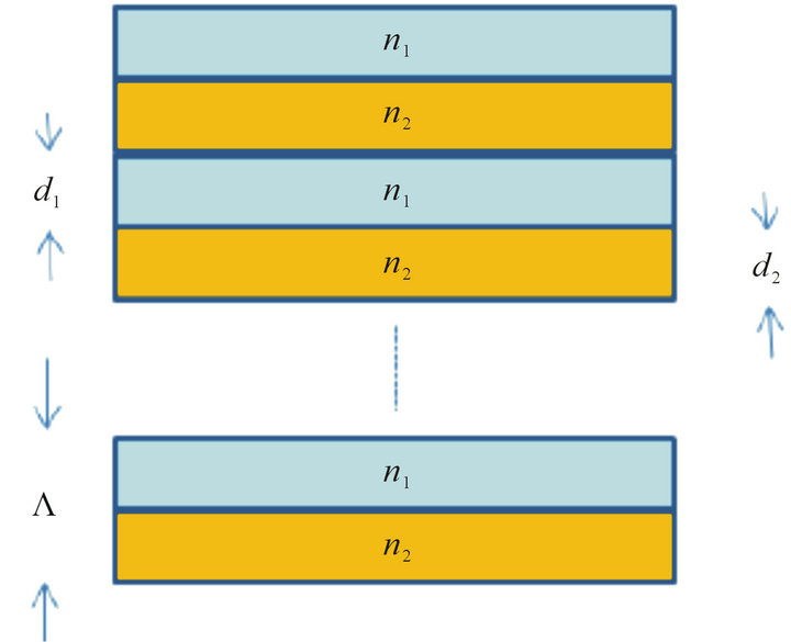
Figure 1. Bragg structure. (n1, n2): refractive index, (d1, d2): layer thickness, Λ: period.
• Number of periods of the multilayer: The number of periods influences on different characteristics of spectrum.
• Thickness of layers : normalized to the period thickness Λ. Thus,
  can range from 0 to 1. The thickness of layer 2 is calculated from using:
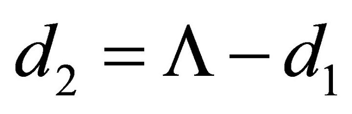 .
.
The spectrum of transmission and reflection calculated for this multilayer is plotted in the left side graph (Figure 2).
2.1. Simulation of Band Diagram
The simulations are made by a code based on the method of plane waves [5]. This method is one of the first methods used, because it is easy to understand and computationally very straightforward to implement. It can be used to solve periodic problems in one, two and three dimensions.
To use this method to study a Bragg structure we will vary the refractive indices n1 and  and thickness of the spacer layer.
2.1.1. Influence of Refractive Index Difference
In this section, we studied the impact of the change in the index difference 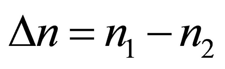 of one-dimensional system which consists of 20 alternating layers of two different materials (GaAs/AlAs), (SiO2/TiO2), (GaAs/Air), (AlAs/Air). Suppose that a plane wave propagating normally (normal incidence) to the layers are the 1D structure, thus it can be decomposed into two independent wave polarizations (parallel and transverse) [4]. The band diagram as a function of the normalized frequency is given afterwards.
As indicated in Figures 3-6, the variation of the refractive index difference influences the position and width of the photonic gaps, increase in this parameter creates a widening of the BIP as demonstrated in (Table 1) and a shift towards higher frequencies (blueshift).
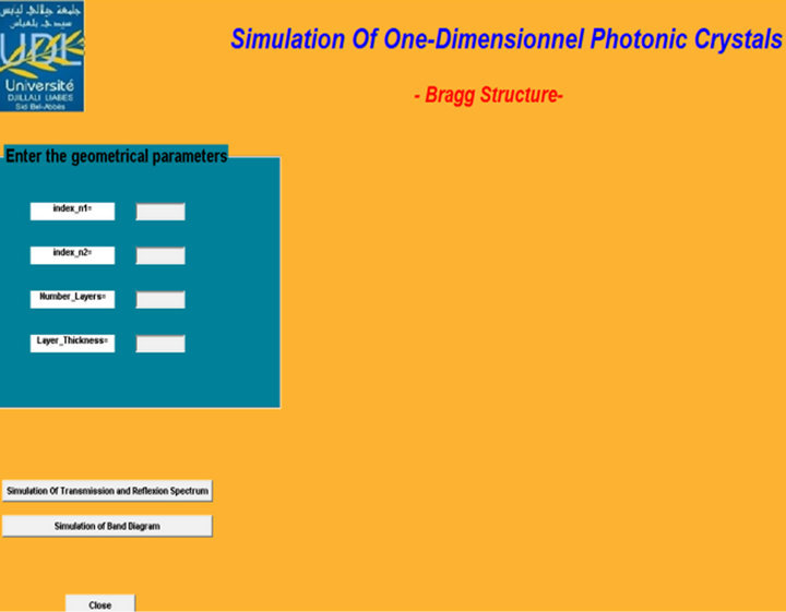
Figure 2. Graphic user interface of simulation.
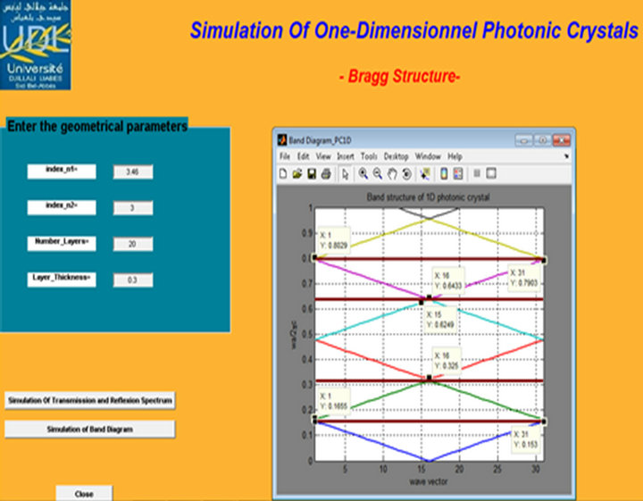
Figure 3. Band diagram of Bragg structure with 20 alternating pairs. H (GaAs)-L (AlAs) n1 = 3.46, n2 = 3 and d1/Λ = 0.3.
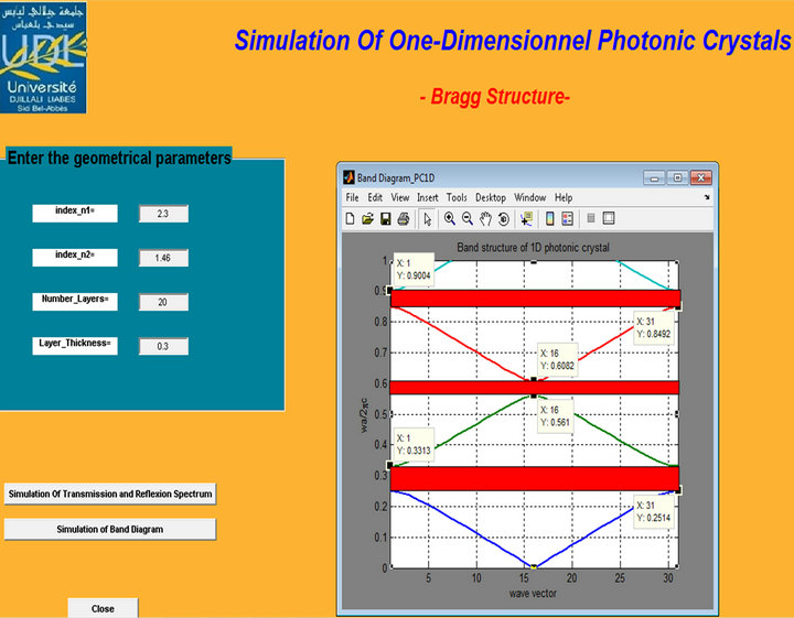
Figure 4. Band diagram of Bragg structure with 20 alternating pairs H (SiO2)-L (TiO2) n1 = 2.3, n2 = 1.46 and d1/Λ = 0.3.
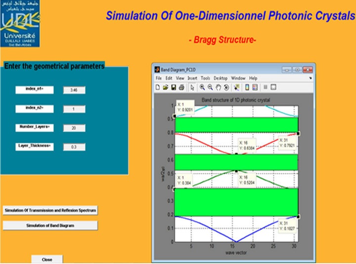
Figure 5. Band diagram of Bragg structure with 20 alternating pairs H (GaAs)-L (air) n1 = 3.46, n2 = 1 and d1/Λ = 0.3.
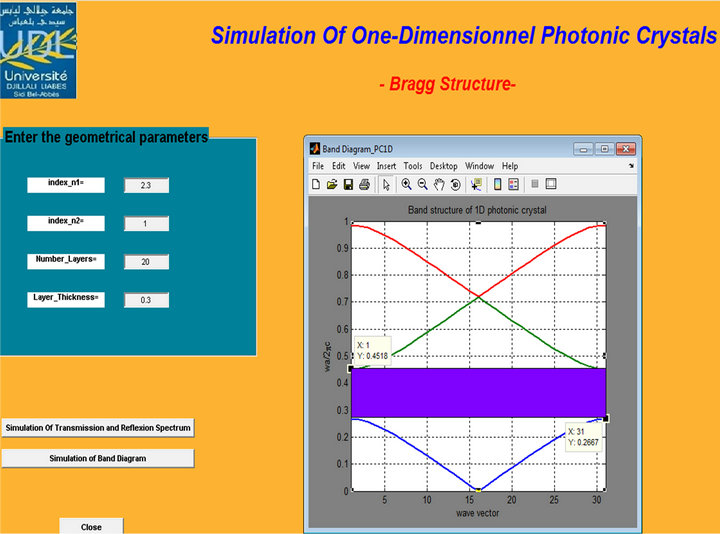
Figure 6. Band diagram of Bragg structure with 20 alternating pairs H (AlAs)-L (air) n1 = 2.3, n2 = 1 and d1/Λ = 0.3.

Table 1. Variation of the availability and width of PBG in function of the refractive index difference.
2.2.2. Influence of Layer Thickness
Now we keep the refractive indices constant (n1 = 3, n2 = 1), Number_layers = 20 and the thickness varies, Layer thickness = 0.4, 0.5, 0.6.
We deduce from the Figures 7-10 the effect of variation in thickness of the layers, the increase in this parameter sets a widening of the BIP (Table 2) and a shift to lower frequencies (redshift).
2.2. Simulation of Transmission and Reflection Spectrum
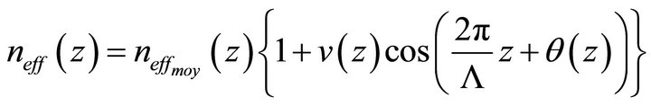
The simulations are made by a code based on the method of coupled waves [6]. This method is one of the first methods used, because it is easy to understand and computationally very straightforward to implement. Generally, a Bragg grating is a periodic modulation of the index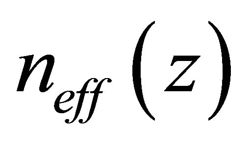 .We can formulate this disturbance index as follows:
 (3)
(3)
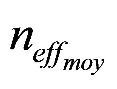 is the average change of the refractive index,
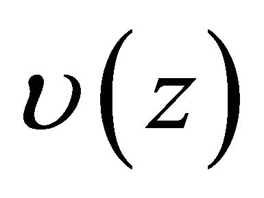 apodisation or visibility of the modulation, the period Λ of the modulation and
  its phase. For our study, we chose the case of a uniform Bragg grating
 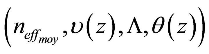 are constants and do not vary. To use this method to study a Bragg structure we will vary the refractive indices
  and
and  and thickness of the spacer layer. The simulations are made by a code based on the method of coupled modes (CMM) [7]. So
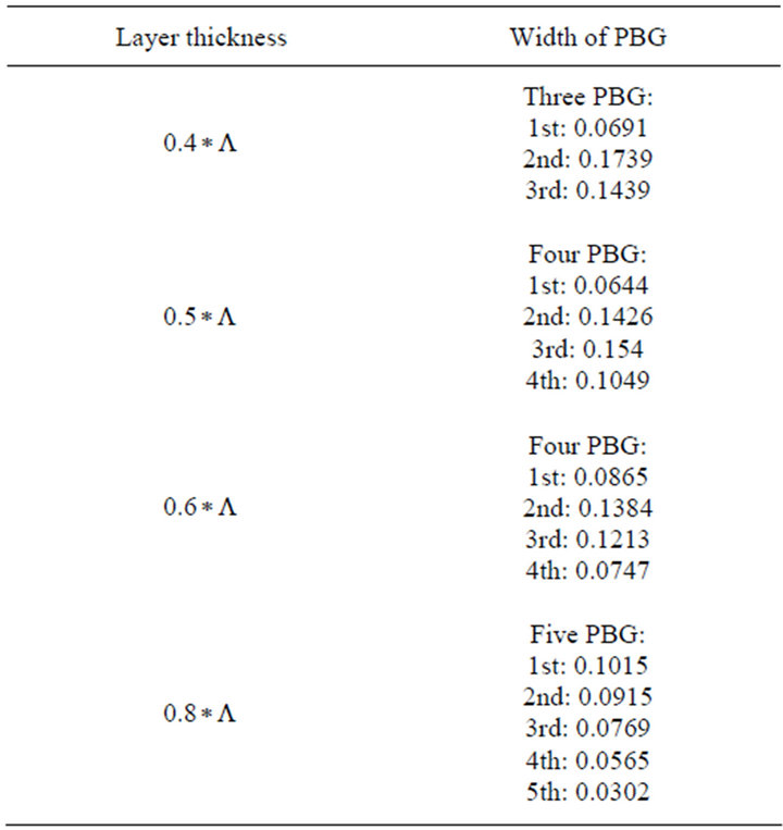
Table 2. Variation of the availability and width of PBG in function of layer thickness.
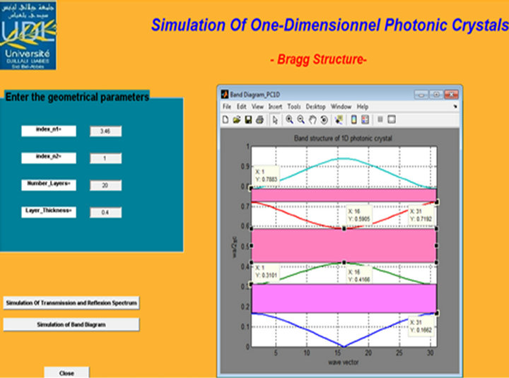
Figure 7. Band diagram of Bragg structure with 20 alternating pairs H (GaAs)-L (air) n1 = 3.46, n2 = 1 and d1/Λ = 0.4.
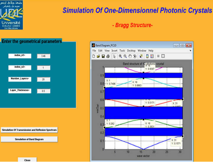
Figure 8. Band diagram of Bragg structure with 20 alternating pairs H (GaAs)-L (air) n1 = 3.46, n2 = 1 and d1/Λ = 0.5.
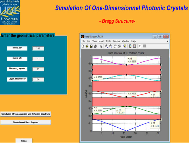
Figure 9. Band diagram of Bragg structure with 20 alternating pairs H (GaAs)-L (air) n1 = 3.46, n2 = 1 and d1/Λ = 0.6.
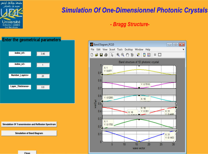
Figure 10. Band diagram of Bragg structure with 20 alternating pairs H (GaAs)-L (air) n1 = 3.46, n2 = 1 and d1/Λ = 0.8.
consider a Bragg grating with:
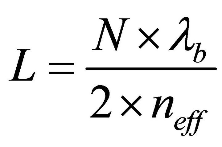
which is the length of the structure, .
.
2.2.1. Impact of the Variation of the Index Difference Δn of the Spectrum Coefficients of Transmission and Reflection
To understand the influence of the change in the index difference  on the spectrum of the reflection (transmission respectively) of one-dimensional system which consists of alternating layers of two different materials (GaAs/AlAs), (SiO2/TiO2), (GaAs/TiO2), while keeping, of course, the other fixed parameters. Suppose that a plane wave propagating normally (normal incidence) to the layers are the 1D structure, thus it can be decomposed into two independent wave polarizations (parallel and transverse) [2].
The width of the spectral band is defined as the width at half-height of the main lobe. It relates to the range of wavelengths for which the structure is highly reflective. The side lobes observed outside the spectral band are due to a Fabry-Perot effect between the two faces of the structure. Increase in the index difference implies a broadening of the photonic band gap as is demonstrated in Figures 11-13 and a shift towards higher wavelengths (redshift). We notice also an increase in the peak reflectivity and a decrease in the transmission (Table 3) [8].
2.2.2. Impact of the Variation of Number Layers of the Spectrum Coefficients of Transmission and Reflection
Now we will see the impact of varying the number of layers (Number_Layers = 5 to 15) on the power transmission and reflection of a wave through a Bragg structure.
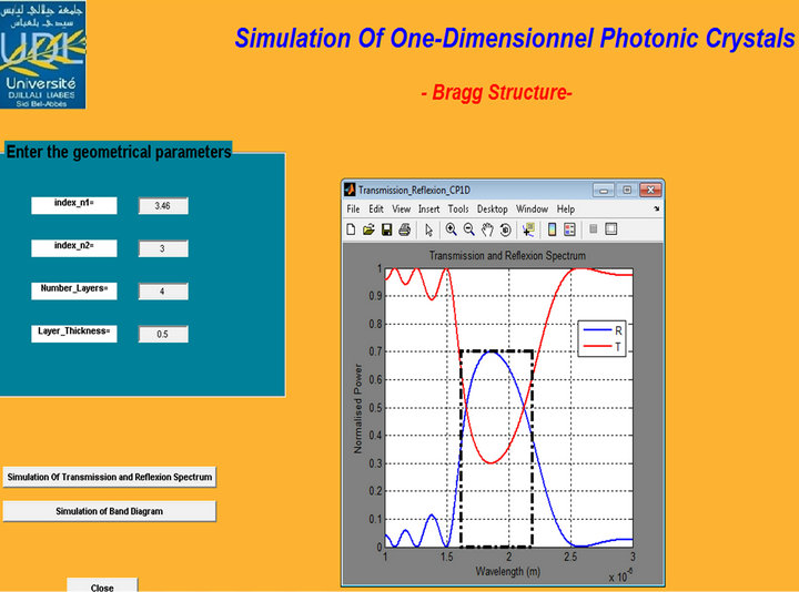
Figure 11. Transmission and reflection spectrum of Bragg structure with 4 alternating pairs H (GaAs)-L (AlAs) n1 = 3.46, n2 = 3 and d1/Λ = 0.5.
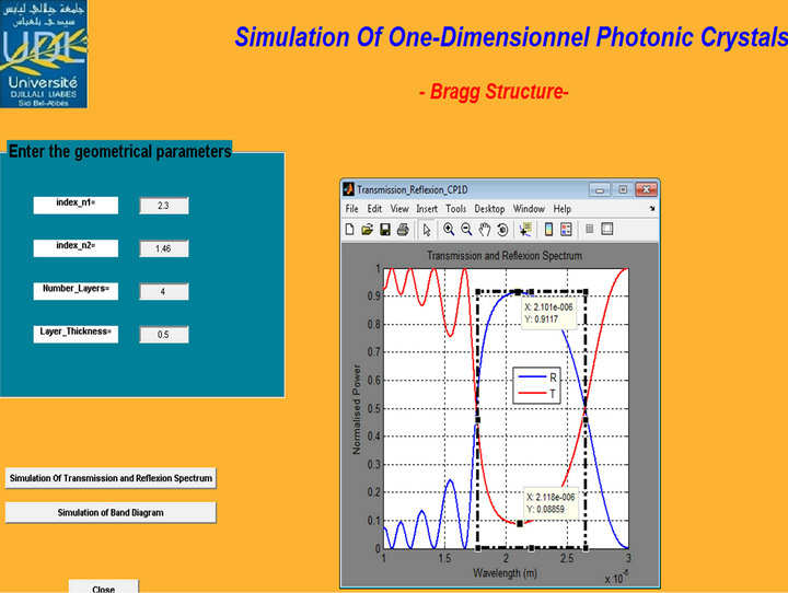
Figure 12. Transmission and reflection spectrum of Bragg Structure with 4 alternating pairs H (SiO2)-L (TiO2) n1 = 2.3, n2 = 1.46 and d1/Λ = 0.5.
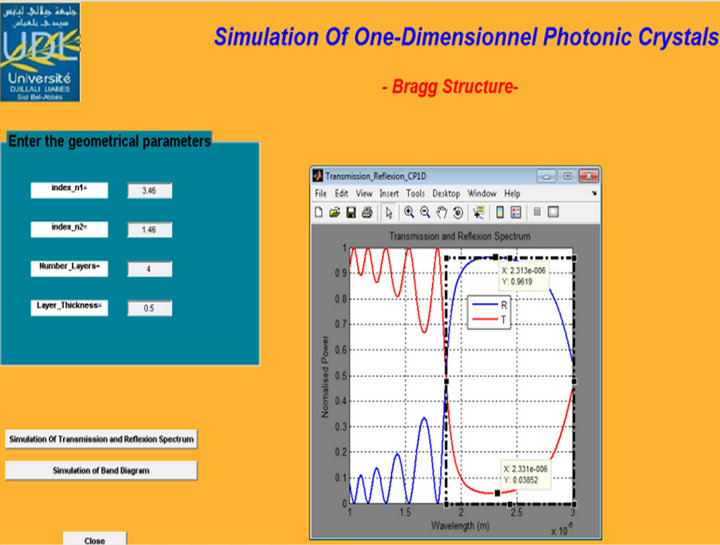
Figure 13. Transmission and reflection spectrum of Bragg Structure with 4 alternating pairs H (GaAs)-L (TiO2) n1 = 3.46, n2 = 1.46 and d1/Λ = 0.5.
As indicated in Figures 14-16, if the number of layers increases (5 to 15), the reflectance approaches unity and the width of the band gap decreases which means that the filter will become increasingly selective.
3. Conclusions
In this paper, we created a graphical interface for calculating the band structure and spectrum of transmission
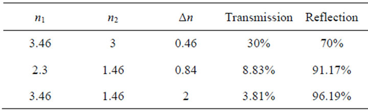
Table 3. Variation of transmission and reflexion in function of refractive index difference.

Figure 14. Transmission and reflection spectrum of Bragg structure with 5 alternating pairs H (GaAs)-L (AlAs) n1 = 3.46, n2 = 3 and d1/Λ = 0.5.

Figure 15. Transmission and reflection spectrum of Bragg structure with 10 alternating pairs H (GaAs)-L (AlAs) n1 = 3.46, n2 = 3 and d1/Λ = 0.5.
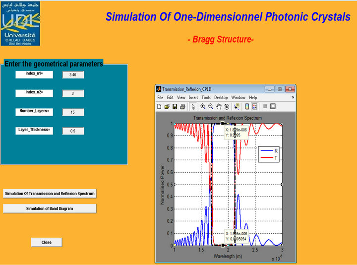
Figure 16. Transmission and reflection spectrum of Bragg structure with 10 alternating pairs H (GaAs)-L (AlAs) n1 = 3.46, n2 = 3 and d1/Λ = 0.5.
and reflectance of Bragg grating by Plane Wave Method and Coupled Wave Method respectively. From simulation results we demonstrate that the width and position of the band gap depends on parameters such as the index difference, number of layers, layer thickness.
These first simulation results are interesting enough that we can consider the realization of device for the benefit of integrated optics.
REFERENCES
- C. Kittel, “Introduction to Solid State Physics,” John Wiley & Sons, New York, 1996.
- M. R. Aced and R. Naoum, “The Photonic Band Gap Materials,” Université Djillali Liabes, Sidi-Bel-Abbes, 2005.
- A. V. Kavokina and M. A. Kaliteevski, “Light-Absorption Effect on Bragg Interference in Multilayer Semiconductor Heterostructures,” Journal of Applied Physics, Vol. 79, No. 2, 1996, pp. 595-598.
- V. E. Borisenko and S. Ossicini, “What Is What in the Nanoworld: Handbook on Nanoscience and Nanotechnology,” Wiley-VCH, Weinheim, 2008, p. 98.
- S. P. Guo, “Plane Wave Expension Method for Photonic Band Gap,” Old Dominian University, Norfolk, 2001.
- http://en.pudn.com/downloads128/sourcecode/math/detail545918_en.html
- M. Suleiman, “Design of an Optoelectronic Sensor by Interferometry SANO-Injection for Demodulating Optical Signals to Optical Fiber Bragg Gratings,” Université de Toulouse, Toulouse, 2008.
- C. Alberto and P. Cham, “Analysis of Photonic Components by Low Coherence Reflectometry Phase-Sensitive,” Graduate School of Computer Science, Paris, 2004.