Energy and Power Engineering
Vol.09 No.04(2017), Article ID:75332,15 pages
10.4236/epe.2017.94B070
The Simulation of Surface Charge Accumulation on PMMA with Different Surface Roughness in Vacuum
Jiyuan Yan1, Jie Ren1, Qing Xie1, Haofan Lin1, Zhiliang Hu1, Huijuan Ran1, Weitao Hu2, Si Li3
1Hebei Provincial Key Laboratory of Power Transmission Equipment Security Defense, North China Electric Power University, Baoding, China
2Hebei Electric Power Corporation maintenance branch, Shijiazhuang, China
3Beijing Electric Power Corporation, Beijing, China


Received: March 8, 2017; Accepted: March 30, 2017; Published: April 6, 2017
ABSTRACT
The surface insulation properties of insulating material under DC voltage are closely related to the characteristics of surface charge accumulation, and the surface roughness of these materials has a direct impact on the surface charge distribution in vacuum. Therefore, it is significant to study their connection. In this paper, based on the secondary electron emission avalanche model, the surface charge accumulation on polymethyl methacrylate (PMMA) with different surface roughness was simulated by using particle in cell and Monte Carlo Collision method. The simulated environment was under the finger shaped electrode and in vacuum. The results showed that under the action of the electric field the electrons emitted from the cathode triple junction moved forward and collided with the insulating material, which may lead to the generation of secondary electrons or the accumulation of surface charge. The surface charge near the cathode was mostly negative since the effect of surface electron injection was greater than that of the collision ionization. Due to the change of electron energy and the influence of electric field distribution, the number of positive charge on the insulator gradually increased, reached the maximum, and then gradually reduced with the approaching of the anode. Moreover, when the surface roughness of the material increases or the secondary electron emission coefficient decreases, the amount of surface charge accumulated on the PMMA will reduce. This paper can provide some guidance for the practical application of insulating materials.
Keywords:
Surface Charge, Secondary Electron Emission, Surface Roughness, PMMA

1. Introduction
Electrical insulation performance plays a significant role in the development of power systems. The vacuum environment is often utilized in power systems due to excellent insulation properties, but the interface between the vacuum and the insulator is the weakness of the entire insulation system. One of the crucial factors is that the surface of the insulating materials tends to accumulate charge under DC voltage and then prone to flashover, which not only affects the operation of the equipment, but also may cause critical economic losses. Therefore, it is of great engineering significance to study the characteristics of surface charge distribution in vacuum.
At present, many scholars have studied the phenomena of the surface charge accumulation by means of measurement or simulation. Given that the charge accumulation process cannot be measured and the experimental comparison is difficult, simulation is a good way to investigate the problem of surface charge accumulation and the methods of particle in cell (PIC) and Monte Carlo Collision (MCC) are usually applied. A considerable amount of research has been done during the last decade. With the aid of COMSOL software, Li built the MCC-PIC model of the actual composite insulator in air and analyzed the accumulation and decay of surface charge [1]. The influence of secondary electron emission and electron beam avalanche movement in the process of flashover in vacuum has been investigated by Liu et al., based on the single particle model and the motion equation of charged particles [2]. Wang et al. studied the dynamic process of SF6/N2 mixed gas discharge through the MCC-PIC method, and considered the process of the ionization, adsorption, recombination and photo ionization of particles [3]. Yu et al. applied Monte Carlo method to study the two dimensional simulation of the surface charge distribution in a plane, a circular and a rectangular symmetric electrode system [4]. The results show that there is a small range of negative charge regions on the surface of the insulator near the cathode, and then it becomes a large positive charge region.
The above researches are of great significance to explore the charge accumulation characteristics of materials. However, it can be seen that there are few researches about the influence of surface roughness on surface charge accumulation in vacuum. Xie et al. and Liu et al. studied the effects of surface morphology on the flashover characteristics under DC voltage and microsecond pulses, but the experimental environment were air [5] [6]. Yamamoto et al. used mechanical grinding to change the surface morphology of the insulator and found that increasing the surface roughness was helpful to improve the dielectric insulation properties [7]. Some people have got different conclusions, that the mapping between surface roughness and dielectric insulation is not monotonically changing related to the material itself [8]. Therefore, the effect of the surface roughness of the insulating material on the surface charge accumulation remains to be studied.
In this paper, the surface roughness of PMMA was characterized by MATLAB, and based on the principle of secondary electron emission the MCC- PIC simulation model was established. The simulation of surface charge accumulation on PMMA with different surface roughness in vacuum was carried out, and the effect of the second electron emission coefficient on the surface charge accumulation with the same roughness was studied.
2. Surface Charge Accumulation Model
2.1. Accumulation Principle
Domestic and foreign scholars have reached an agreement on the understanding of initial stage, where the cathode three junction (CTJ) generates the initial electrons, and final stage, where the flashover is performed in the desorbed gas layer near the surface of the insulator or in the near surface layer of the solid dielectric, about the flashover process of insulating materials in vacuum. However, it is not very clear for the intermediate process of flashover development and many hypotheses exist. In this paper, the secondary electron emission avalanche (SEEA)model, which is widely used in vacuum, was applied to simulate the collision process between electrons and the surface of insulating material, and this paper combined with the method of simulating the motion of particles (i.e. MCC-PIC) to achieve the dynamic simulation of charged particles. This model describes the intermediate process of the surface flashover of the insulator as the initial electrons emitted from CTJ will bombard the surface of the insulator, which can lead to secondary electron emission and doubling. Meanwhile, the surface of the material may accumulate charge during this process.
2.2. Simulation Arrangement
Figure 1 illustrates the simulation arrangement. The electrodes utilized in this research were made of stainless steel and presented as ‘finger’ type, i.e. the front of the electrode was hemispherical in shape with a radius of curvature of 7.5 mm. And the distance between the two electrodes was 8 mm. The size of the insulating material was 1.5 mm × 40 mm and the size of the substrate made of PTFE was13.5mm×40mm. The corresponding blank area in the dashed box was the solution space studied in the simulation, and the environment was in vacuum. In the simulation, the material of the insulator was PMMA, whose permittivity was 3.7. In addition, the right electrode was grounded and the left electrode was applied with a voltage of −10 kV.

Figure 1. Geometric model.
For the selection of the initial free-moving electronic position, the CTJ electric field strength of the insulator is relatively large, prone to field emission and more likely to produce electrons, as shown in Figure 2. So it was chosen to apply a certain number of electrons with a certain initial kinetic energy at the CTJ.
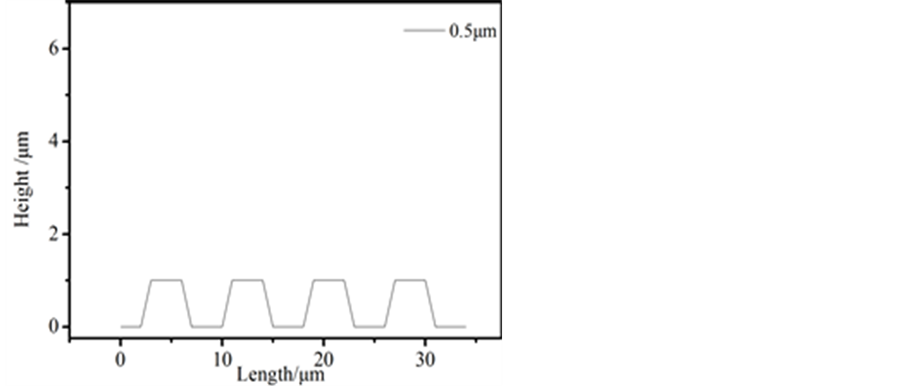
In order to further study the effect of the surface roughness of the insulating material on the surface charge accumulation process, the periodic square wave function was selected to characterize the surface roughness of PMMA surface profile, as shown in Figure 3. According to the definition formula of the surface roughness characteristic parameter named Ra, that is the arithmetic mean value of the absolute value of the contour deviation within the sampling length. The surface roughness of the surface to be constructed was about 0 μm, 0.5 μm and 3 μm, respectively.
2.3. MCC-PIC Simulation
The basic idea of MCC-PIC simulation is as follow. Firstly, the corresponding spatial electric field distribution can be obtained through solving the Poisson equation in the presence of charged particles. Then the motion of the particle is tracked by solving the Newton motion equation which describes the particle motion in vacuum, and the Maxwell equation [9]. Based on the SEEA model, the MCC method is used to simulate particle collisions. Continuously circulate the above process until the electron motion is beyond the range of the study area or the movement reaches the other side of the electrode surface to stop. It is worth noting that each cycle will push the particles into the new position and give the new speed.

Figure 2. Electric field distribution without space charge.
 (a)
(a)
 (b)
(b) (c)
(c)
Figure 3. Construction of PMMA surface roughness. (a) Ra = 0 μm; (b) Ra = 0.5 μm; (c) Ra = 3 μm.
This process is a good way to achieve a tracking simulation of the motion of charged particles. The flow chart of the specific model is shown in Figure 4.
The electric field region is discretized into a finite number of nodes by using the finite element method, and then the information of electric field is calculated. Finally the approximate description of electric field is obtained. The variational problem of two-dimensional Poisson field can be expressed as follows:
 (1)
(1)
 (2)
(2)
where
φ is the electric potential distribution;
ε is the permittivity of the medium;
ρ is the charge density;
φ0 is the electric potential of electrodes.
The PIC simulation is based on the equation of motion. Gradually updated the displacement and velocity of the charged particle according to the unit time step Δt. The dynamic equations of motion of the charged particles can be expressed as follows:
 (3)
(3)
where
q is the amount of charge of particles;
m is the mass of charged particle;
 is the electric field strength at the position of charged particle.
2.4. The SEEA Model
When the electrons move to the surface of the insulating material, it may be adsorbed or collided to produce secondary electrons. The secondary electron emissivity of the insulating material represents the ratio of the number of secondary electrons to the number of primary electrons, which is determined by the electron energy colliding on the material surface, i.e., δ = φ(ε). The emissivity curves of the secondary electrons with the change of the primary electron energy are shown in Figure 5.
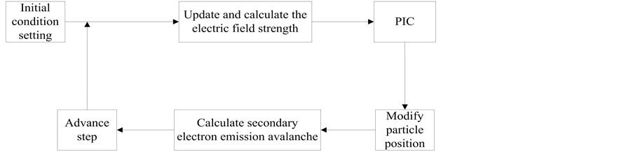
Figure 4. The flow chart of MCC-PIC simulation.
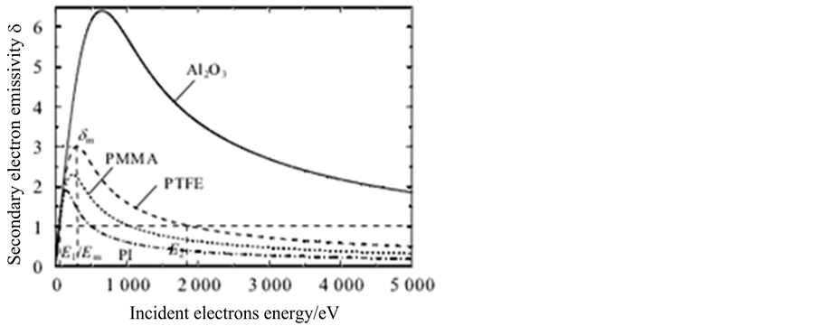
Figure 5. The curve of secondary electron emissivity.
As can be seen from Figure 5, for a particular insulating material, when the primary electron energy is known, the corresponding secondary electron emissivity can be obtained. Because the insulating material chosen in the simulation model is PMMA, the secondary electron emissivity of PMMA can be approximated according to the range of electron energy, and the approximate results are shown in Table 1.
When δ is greater than 1, the secondary electron emission caused by incident electrons makes the surface of the insulating material corresponding to positive charges; When δ is zero, the incident electrons are adsorbed on the surface of the insulating material and it leads to electronegativity of surface; When δ is 1, the secondary electrons are equivalent to the scattered electrons of the primary electron.
The second electron energy ε follows a certain probability density distribution, and the determination of the secondary electron energy is carried out according to the random sampling of the corresponding distribution. The direction of motion of electrons, however, is determined according to cosine distribution. When the secondary electrons move in the gas space between the electrodes, the electrons are accelerated by the combined action of external electric field and electric field generated by the accumulated charges. Part of the secondary electrons produced on the surface are still likely to hit the insulator surface again and cause the new secondary electrons to emit.
2.5. Particle Position Correction
In the tracking process of charged particles, when the displacement and velocity of the charged particles are gradually updated each iterative step Δt, the particles may collide with the insulating material or electrode in a certain step. At the same time due to the appearance of rough surface, the secondary electrons may repeatedly collide with the interface in the “trap”, as shown in Figure 6. At this point, there is a problem with the position and energy of the particle obtained by PIC simulation at the step length of Δt, and it needs to be modified.
 (a)
(a) (b)
(b) (c)
(c)
Figure 6. Collision mode: (a) In the material; (b) In the gas space; (c) In the electrode.

Table 1. Secondary electron emissivity of PMMA surface.
For the modification of particle, the time interval from the last movement to the occurrence of the collision need to be solved, and then the data should be modified to obtain the position and energy of the moment when electrons impact insulating material. In this case, the following two cases are considered: one is according to the kinetic equation, that the position of the particle is judged to be inside the insulating material after the time step Δt, as shown in Figure 6(a); another is that the position of the particle is judged to be above the insulator surface after the time step Δt, that is in the gas space. As we can see from the Figure 6(b), the illusion appears that electrons do not collide with material interface. When either occurs above, it is necessary to modify the position and energy of the electron in order to more accurately consider the influence of the surface morphology of the insulating material on the surface charge accumulation.
For the case of Figure 6(a), the position of the particles after the unit step is in the insulating material. Taking this moment as the end point and the period moment as the start point, the simultaneous motion equation and the surface roughness function are used to solve the intersection coordinates, and the equation is based on dichotomy for numerical calculation. For the case of Figure 6 (b), the particle is located in the gas space after the unit step, but it collides with the insulating material actually. Choosing the location of the previous moment as a start point, the intersection point of the first collision with the insulating material interface is searched iteratively. Based on these methods, the relevant information of the particles can be modified. Figure 6(c) shows the phenomenon of particles moving to the electrode after modification. The field strength of the particle position is taken as the basis for judging the position of the particle. If the electric field strength is zero, it means electrons move to anode, and it is no longer necessary to trace the electrons. For the particles moving to the outside of the study area, ignoring the effect of the distortion of the electric field, all the information of the corresponding particles will be deleted.
3. Surface Charge Accumulation Simulation
3.1. Influence of Surface Roughness on Surface Charge Accumulation
200 electrons with initial kinetic energy were applied at CTJ, and the simulation of surface charge accumulation was carried out using the materials with 0 μm, 0.5 μm, and 3 μm roughness which was constructed above.
The results of surface electrons and positive ions of three surface roughness materials are shown in Figure 7 and Figure 8. The number of particles in the corresponding position of Figure 7 and Figure 8 was superimposed to obtain the number of particles on the surface of the insulating material, as shown in Figure 9. The orthogonal decomposition of the surface electric field is shown in Figure 10.

Figure 7. Distribution of electrons.

Figure 8. Distribution of positive ions.

Figure 9. Distribution of apparent particles number.

Figure 10. Material surface electric field.
It can be seen from Figure 7 and Figure 8 that the electrons and positive ions are mainly concentrated on the side of the insulating material near the cathode, and the number of particles accumulated near the anode is small and dispersed. Figure 9 indicates that there is a small amount of negative charge near the cathode, and that the number of positive ions gradually increases, reaches the maximum, and then gradually decreases with the approaching of the anode.
That is because, for the electrons which collide closer to the cathode position, although the front electrode of the electric field strength is large, the acceleration distance before collision is not long enough which results in the lack of electronic energy. Most of the electrons have energy in the 0 eV - 28 eV interval of the secondary electron emissivity curve of PMMA, which will be directly adsorbed on the surface of the material when it collides with the material. Therefore, on the whole, the cathode front of the material surface accumulates negative charge. As the position that the electrons impact material is farther away from the cathode, the acceleration distance of the electrons before collision is longer and the speed is larger. At this time, most of the electron energy is in the 28 eV - 3000 eV interval of the secondary electron emissivity curve of PMMA. When a high- energy electron collides with the material, the surface of PMMA will generate secondary electrons, so the material surface will gradually show positive polarity. With the further increase of the collision distance, that the normal electric field on the surface of the material gradually reversed, coupled with the influence of electronic jump, will cause the distortion of electric field on the surface of insulating material, resulting in the less surface charge accumulation near the anode. Comparing the effects of different voltages on the surface charge accumulation, it is found that when the voltage is high, the amount of charge accumulated on the surface will increase accordingly, and the above phenomenon is more obvious.
Ding et al. applied an experimental device similar to this simulation model to measure the surface potential distribution of the material before nanosecond pulse flashover [10]. Similarly, they found that the surface of the sample had positive charge and the cathode potential was higher than the anode potential. It was considered that the secondary electron emission played a major role in the process of charge accumulation. Yu et al. simulated the surface charge two-di- mensional distribution of the insulator before flashover in vacuum [4]. The results show that the surface of the dielectric near the cathode has a small range of negative potential and then becomes a large area for positive charge.
In addition, it can be seen from Figure 7 and Figure 8 that the amount of positive and negative charge on the surface of the material decreases with the increase of the roughness in vacuum. That is because when the surface roughness of the material increases, the rugged surface morphology is relatively more and more obvious. The emergence of micro-slot will lead to electrons ejecting repeatedly in the tank, which will reduce the energy of electrons, restrain the movement of electrons and hinder the transition of electrons. The uneven surface of the material also increases the probability of the occurrence of diffuse reflection. The changes of the space electrons are as follows. With the movement of electrons to the anode, the number of electrons near the PMMA surface is relatively reduced, and the development of the electron avalanche is suppressed, resulting in the reduction of the number of electrons. Yamamoto et al. studied the surface charge accumulation after the insulator applied voltage with different surface roughness in vacuum, and found that the amount of charge on the surface of the material decreased with the increase of the roughness, which was similar to the view of this paper [11]. It proves the correctness of this simulation from a certain extent.
3.2. Effect of Secondary Electron Emissivity on Surface Charge Accumulation
The surface characteristics of the insulating material will be changed after surface attrition treatment. Some studies have indicated that the secondary electron emissivity will be different after the surface roughness changes [8] [12]. Taking the material surface roughness Ra = 0.5 μm as an example, the influence of the secondary electron emissivity on the surface charge accumulation was explored by changing the secondary electron emissivity curve of the material and the other conditions were the same as above. The secondary electron emissivity of the three different materials of “low”, “medium” and “high” is shown in Table 2, where “medium” is the PMMA secondary electron emission curve used in the model established above.
The results of simulation and calculation about the distribution of surface electrons and positive ions were shown in Figure 11 and Figure 12. The number of particles in the corresponding positions of Figure 11 and Figure 12 is superimposed to obtain the number of particles viewed on the surface of the insulating material as shown in Figure 13.
It can be seen from Figure 11 and Figure 12 that the number of electrons and positive ions accumulated on the surface of the material increases as the second-

Figure 11. Distribution of electrons.

Figure 12. Distribution of positive ions.

Figure 13. Distribution of apparent number of particles.
Table 2. Secondary electron emissivity.
ary electron emissivity increases. As shown in Figure 13, the number of apparent particles is similar to that of the preceding text, so the reasons will not repeat. For the electronic movement of different insulating materials, the larger the secondary electron emissivity is, the more the number of electrons emitting from the surface of the material is, the faster the electron avalanche develops, and the more the number of electrons in space is. Therefore, by reducing the secondary electron emissivity of the insulating material or selecting a material which has a smaller secondary electron emissivity, the accumulation of the surface charge can be weakened to some degree. Miller had conducted a similar experiment, that the Cr2O3, which had a smaller secondary electron emission coefficient, was coated on the surface of the Al2O3, and he found that the flashover voltage was improved, which can prove the correctness of the simulation to a certain extent [13]. It should be noted that increasing the surface roughness of the material will reduce the amount of the surface charge. In terms of this increasing the surface roughness of the material contributes to the increase of the insulation properties of the material. However, the change of the surface roughness of the material will also affect the secondary electron emission coefficient. Therefore, in practical applications, the material should be treated in integrated consideration of the effects of roughness and secondary electron emissivity.
4. Conclusions
In this paper, the different surface roughness of PMMA was characterized by MATLAB, and the MCC-PIC simulation model was established. Based on the principle of secondary electron emission, the simulation of the surface charge accumulation of the PMMA in vacuum was carried out, and the influence of the second electron emission coefficient on the surface charge accumulation under the same roughness was studied. The main conclusions are as follows:
1) The electrons emitted from the CTJ were developed in terms of the second electron emission avalanche model. Then the charge accumulation was generated on the surface of the material. The effect of the electronic adsorption and injection on the surface of the material near the cathode was greater than that of the collision ionization, resulting in more negative charge on the surface. Due to the change of electron energy and the influence of electric field distribution, the surface of the material gradually showed positive polarity accumulation. The number of positive charge gradually reached the maximum, and then progressively reduced with electrons approaching the anode.
2) When the surface roughness of the material was changed, the surface charge accumulation of the material was affected, and the larger the surface roughness of the material was, the less the surface charge accumulated.
3) When the secondary electron emission coefficient of the material was changed, the charge distribution on the surface of the material was affected, whilst the smaller the secondary electron emission coefficient was, the less the surface charge accumulated.
Acknowledgements
This work was supported in part by Natural Science Foundation of Hebei Province (Grant No.E2015502081), and Fundamental Research Funds for the Central Universities (Grant No. 2016ZZD07), and State Key Laboratory of Alternate Electrical Power System with Renewable Energy Sources (Grant No.LAPS16009), and the National Natural Science Foundation of China (Grant No. 51507066).
Cite this paper
Yan, J.Y., Ren, J., Xie, Q., Lin, H.F., Hu, Z.L., Ran, H.J. and Hu, W.T. and Li, S. (2017) The Simulation of Surface Charge Accumulation on PMMA with Different Surface Roughness in Vacuum. Energy and Power Engineering, 9, 644-658. https://doi.org/10.4236/epe.2017.94B070
References
- 1. Li, Z. (2014) Simulation of Surface Charge Accumulation on High Voltage DC Composite Insulator. M.D. Thesis, Hunan University, Changsha.
- 2. Liu, Y., Deng, J.J., Wang, M., Zou, W.K. and Zhou, L.J. (2010) Numerical Simulation of Vacuum Surface Flashover under Applied Magnetic Field. High Power Laser and Particle Beams, 22, 2501-2504. https://doi.org/10.3788/HPLPB20102210.2501
- 3. Wang, F., Xiao, X.L., Zhang, X.B., Fu, T.T., Wang, Q. and Zhang, G.X. (2011) Research on the Insulator Surface Discharge Characteristics in SF6/N2 Gas Mixture Using PIC Method. Transactions of China Elec-trotechnical Society, 26, 220-226.
- 4. Yu, K.K., Zhang, G.J., Zheng, N., Zhao, W.B. and Qiu, S. (2008) Two-Dimensional Simula-tion of Surface Charge Distribution on Insulator Prior to Flashover in Vacuum. Journal of Xi’AnJiaotong University, 42, 476-480.
- 5. Xie, Q., Lu, L., Ren, J., Yan, J.Y. and Wang, T. (2017) Research on Creeping Discharge Parameters and Surface Characteristics of PMMA under DC Condition. Insulating Materials, 50, 55-60+67.
- 6. Liu, X., Lin, H.D., Liang, Y.M., Zhang, C., Xie, Q. and Shao, T. (2015) Effect of Atmospheric-Pressure Microsecond Pulsed Discharges on Epoxy Resin Surface. Transactions of China Electrotechnical Society, 30, 158-165.
- 7. Yamamoto, O., Takuma, T., Fukuda, M. and Nagata, S. (2003) Improving Withstand Voltage by Roughening the Surface of an Insulating Spacer Used in Vacuum. IEEE transactions on dielectrics and electrical insulation, 10, 550-556. https://doi.org/10.1109/TDEI.2003.1219636
- 8. Ding, L.J. (2001) Study on the Surface Pre-Flashover and Flashover of Insulators in Vacuum. Ph.D. Thesis, North China Electric Power University, Beijing.
- 9. Liu, J. and Raju, G.R.G. (1992) Evaluation of Transport Coefficients in Nitrogen by the Monte Carlo Method. Journal of the Franklin Institute, 329, 181-194. https://doi.org/10.1016/0016-0032(92)90107-R
- 10. Ding, M., Cheng, Y.H., Yin, W., Wang, Z.B., Chen, Y., Zhou, J.B. and et al. (2009) Surface Charge Properties of Epoxy Composite under Nanosecond Pulsed Voltages. High Voltage Engineering, 35, 157-162.
- 11. Yamamoto, O., Takuma, T., Hamada, S., Kakehashi, Y., Ikoma, S., Nishimura, K., and Shioiri, T. (2001) Influence of Surface Roughness on the Charging of Insulating Spacers in Vacuum. Electrical Engineering in Japan, 135, 16-25. https://doi.org/10.1002/eej.1029
- 12. Yu, K.K., Zhang, G.J., Mu, H.B., Zheng, N., Huang, X.Z., Ma, X.P. and et al. (2012) Effect of Different Surface Treatment on the Surface Flashover Characteristics of Machinable Ceramic in Vacuum. Transactions of China Electrotechnical Society, 27, 115-120.
- 13. Miller, H.C. (1980) Improving the Voltage Hold off Performance of Alumina Insulators in Vacuum through Quasi Metallizing. IEEE Transactions on Electrical Insulation, 5, 419-428. https://doi.org/10.1109/TEI.1980.298336