Materials Sciences and Applications
Vol.4 No.12(2013), Article ID:41128,6 pages DOI:10.4236/msa.2013.412102
Effect of Zn Sputtering Rate on the Morphological and Optical Properties of ZnO Films
![]()
1Technological Plasmas Laboratory, São Paulo State University-UNESP, Sorocaba, Brazil; 2Group of Advanced Materials, São Paulo State University-UNESP, Bauru, Brazil.
Email: *jrborto@sorocaba.unesp.br
Copyright © 2013 Michel Chaves et al. This is an open access article distributed under the Creative Commons Attribution License, which permits unrestricted use, distribution, and reproduction in any medium, provided the original work is properly cited.
Received September 8, 2013; revised October 27, 2013; accepted November 19, 2013
Keywords: ZnO Thin Films; Surface Morphology; Optical Properties; OES
ABSTRACT
Zinc oxide (ZnO) thin films were deposited onto glass substrates by reactive radiofrequency (RF) magnetron sputtering using a metallic zinc target. Optical emission spectroscopy (OES) was used to monitor and control the Zn sputtering rate for the deposition of the ZnO films. Film thicknesses ranged from 350 to 750 nm. Optical transmittances greater than 80% were observed in the wavelength interval from 450 nm to 650 nm. The energy gap of the films remained constant at (3.28 ± 0.01) eV. The surface morphology was found to be homogeneous with well-distributed structures. Surface roughness was dependent on the Zn sputtering rate, indicating that greater densities of Zn atoms increase the surface diffusion. X-ray diffraction (XRD) analysis showed that the ZnO films were polycrystalline with a hexagonal wurtzite structure and preferential growth along the (002) plane.
1. Introduction
Thin films of transparent conductive oxides, known as TCOs (Transparent Conducting Oxides), have several applications in optoelectronic devices. These thin films can be applied especially in organic light emitting diodes (OLEDs), heat mirrors, solar cells and thin film transistors (TFTs) [1]. One of the most studied and industrially used TCOs is tin-doped indium oxide (ITO) [2]. Associated with a recent increase in consumption by the optoelectronic devices industry, however, the element indium has become scarce and more costly. A highly promising candidate to replace ITO is zinc oxide (ZnO) [1,2] due to its advantages such as low cost, non-toxicity and good chemical stability in plasma processing [1,2].
Several techniques have been used for the synthesis of the ZnO thin films such as thermal evaporation [3], laser ablation [4], metal organic chemical vapor deposition (MOCVD) [5], molecular beam epitaxy [6] and magnetron sputtering [7]. Radiofrequency magnetron sputtering is especially interesting because it produces high quality polycrystalline films, allows synthesis at low temperatures (including room temperature), and permits coverage of large substrates. In this work, ZnO thin films were deposited by reactive RF magnetron sputtering, and the rate of sputtering of atoms of Zn was controlled using optical emission spectroscopic monitoring of the plasma environment. The surface texture, optical and structural properties were systematically investigated as a function of the zinc sputtering rate.
2. Experimental Details
Films were deposited onto glass substrates with dimensions of 10 × 30 mm2 and a thickness of 1 mm. The substrates were cleaned according to the following procedure. First they were immersed in an ultrasonic bath (Ultrasonic Clear CBU-100) in a beaker of distilled water with powder detergent (det limp S32). Then they were given a bath with distilled water in the ultrasonic vat. Finally, they were immersed in an ultrasonic bath of isopropyl alcohol, and were blown dry in a warm air stream. For the deposition of thin films of ZnO a system consisting of a cylindrical stainless steel chamber of 270 mm diameter and height 200 mm, equipped with two parallel electrodes of 100 mm diameter and separated by a distance of 40 mm, was used. To control the gas flow needle valves (Edwards, model LV-10K) and mass flowmeters (MKS 1179A) were used. The chamber pressure was monitored by a Pirani pressure sensor (KJL 945). The deposition chamber was evacuated using a rotary vane pump (Leybold D25B). For the excitation of the plasma an RF source (13.56 MHz, maximum power 300 W) was coupled to the target holder. The parameters used for the synthesis of thin ZnO films were a flow rate of 0.08 sccm of oxygen and a total pressure of 1.4 Pa. The sample holder was heated to a temperature of 100˚C and the deposition time was 60 min. A target of metallic zinc (99.995% purity) with 76.2 mm diameter and 3 mm in thickness was employed.
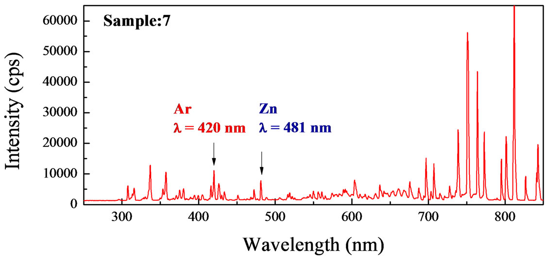
The sputtering rate of Zn was investigated using Optical Emission Spectroscopy (OES) employing a SD 4000 model spectrometer (Ocean Optics, USA). Thus, we monitored the intensities of the emission lines at 481 nm and 420 nm to determine the concentration of metallic zinc (Zn) and argon (Ar) species, respectively, in the plasma environment. In turn, control of the rate of sputtering was carried out by varying the RF power coupled to the plasma around 70 W.
The morphological properties of the films were investtigated using an XE-100 Atomic Force Microscope (Park Systems, USA). Thickness measurements were made using a Dektak profilometer from Veeco Instruments (Model 150). Optical properties were determined from the transmission spectra obtained using an Ultraviolet-visible near infrared spectrometer, model 750 (from Perkin-Elmer, USA). The X-ray diffraction (XRD) measurements were performed employing an X-ray diffracttometer (model D/MAX-2100DC Rigaku, Japan) using CaKα radiation, whose wavelength (λ) corresponds to 1.5405 Å. This approach allows the identification of the film structure, crystal orientation and the average grain size.
3. Results and Discussions
Table 1 shows a summary of the results of the deposition rate, thickness, surface roughness, and band gap, as a function of the ratio of the intensities of spectral emission lines of Zn (481 nm) and Ar (420 nm), ie,  , of the plasma.
During the plasma discharge, the relative concentration of a particular species in the fundamental state can be estimated by measuring the intensities of the spectral lines of the species with known concentration and species with unknown concentration [8]. In this case, the concentration of zinc atoms [Zn] may be estimated from the ratio between the intensities of the emission lines of Zn and Ar as shown by Equation (1):
 (1)
(1)
where IZn and IAr are the emission intensities of the zinc and argon species, respectively, [Ar] is the argon concentration and k is a constant. As illustrated in Figure 1(a), which shows a typical emission spectrum obtained in this work, we used the 481 nm spectral line of Zn and the 420 nm of argon (Ar) to calculate the relative concentration of zinc atoms.
Moreover, in the case of sputtering of metal targets it is expected that the concentration of atoms in the plasma phase is proportional to the sputtering target area. Also, in the case of the deposition of oxide films the growth rate (RG) should be proportional to the sputtering rate, if there is enough oxygen for the formation of a stoichiometric film. Accordingly, Figure 1(b) shows a graph of the growth rate of ZnO as a function of the ratio . Note that the thickness increases linearly with the ratio
  to 0.37. Considering the linear dependence
 (2)
(2)
the linear fit of the experimental data imply a = 25 ± 1 nm/min e b = 3.4 ± 0.3 nm/min, with R2 = 0.988 in the range up  = 0.37. This reinforces the proposition of proportionality between the ratio IZn/IAr and the sputtering rate.

Table 1. Measurements of the growth rate, thickness, surface roughness and optical band gap as a function of the ratio  in the plasma.
 (a)
(a)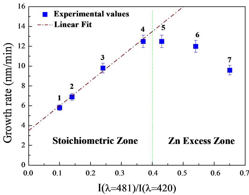 (b)
(b)
Figure 1. (a) Optical emission spectrum of the plasma. The lines of Zn and Ar employed for calculating the ratio  and controlling the rate of sputtering are shown. (b) Graph the growth rate of ZnO as a function of the ratio
 .
.
For values of the ratio  above 0.43, the growth rate of ZnO gradually decreases. This behavior is due to the increased concentration of Zn atoms above the stoichiometric value for the formation of zinc oxide films. In this case, the zinc in excess reduces the concentration of oxygen available for forming the film, causing the observed fall in growth rate. The same effect was reported by Wallendorf et al. [9]. In particular, they show an approximately linear increase in thickness with increasing sputtering rate followed by a decrease in film thickness due to desorption of Zn atoms. However, the thickness increases again when the sputtering rate becomes higher than the desorption rate. For these values, the film formed on the surface of the substrate is practically all zinc, resulting in a metal film.
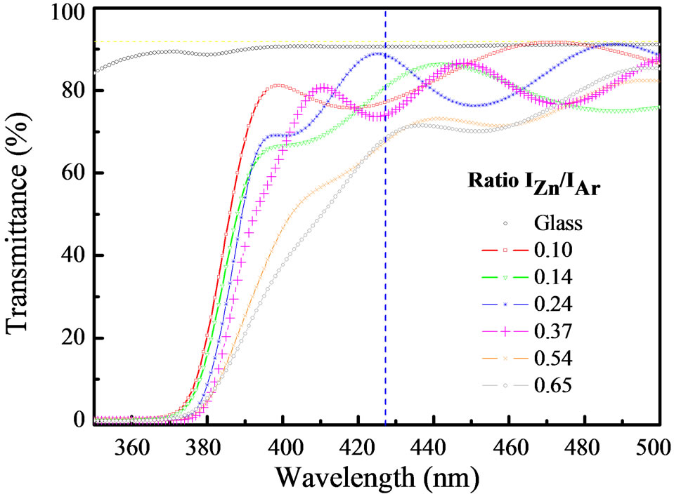
Figure 2(a) shows the optical transmission spectra for the films of ZnO. The films exhibited optical transmittances above 80% for wavelength between 450 and 650 nm. The energy value of the optical gap of the films was around (3.28 ± 0.01) eV. This value is in agreement with data reported in the literature [10]. The absorption edge, however, became greater at greater sputtering rates. It is observed that the transmittance near the absorption band tends to decrease with the value of the ratio  [9]. For values above 450 nm, however, the transmittance curves are the same for all values of
 .
.
The optical behavior is mainly due to incorporation of interstitial zinc atoms in the ZnO matrix. Figure 2(b) shows a diagram of the electronic energy transitions theoretically calculated for various types of defects in a matrix of zinc oxide [11]. From this diagram, it can be seen that the presence of the interstitial Zn atoms promotes a state energy of 2.9 eV, which corresponds to a wavelength of 427 nm. Therefore, it is expected that with the increase of the sputtering rate for zinc above the stoichiometric value, there will be a reduction in the
 (a)
(a) (b)
(b)
Figure 2. (a) Transmittance of ZnO films grown at different ratios of zinc sputtering on glass substrates. (b) Energy transition diagram of ZnO [11].
growth rate as well as the formation of Zn defects in the ZnO matrix. Consequently, the absorption band is broader for values around 2.9 eV.
The surface morphology of the films was investigated using atomic force microscopy (AFM). Figure 3 shows AFM images of square regions of side length 2 µm for the samples described in Table 1.
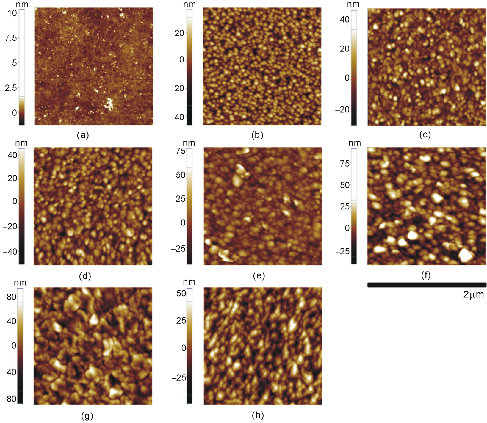
Figure 3. AFM images of ZnO. (a) Glass substrate, (b)  = 0.10, (c)
  = 0.14, (d)
  = 0.24, (e)
  = 0.37, (f)
  = 0.43, (g)
  = 0.54 e (h)
  = 0.65.
It is observed in the AFM images, that all the ZnO films exhibit a very homogeneous distribution of grains. In the AFM images of Figures 3(b) to 3(d), it can be seen that the films have a surface morphology with grain structures of essentially spherical geometry, when deposited in stoichiometric conditions. From Figures 3(e) to 3(h), or when there is excess Zn, a slight change in shape of the grains, passing from spherical to irregular, is observed.
Figure 4(a) shows XRD spectra of the ZnO samples deposited from plasmas with different  values. The spectra show a peak, indicating a preferred crystallographic orientation in the (002) plane. This peak corresponds to the hexagonal wurtzite structure of ZnO, which grows along the c-axis and perpendicular to the substrate surface [12]. The identification of the crystalline phase was made using data from the standard JCPDS (Joint Committee on Powder Diffraction Standards) table. The average crystallite size (
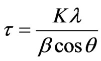
 ) was determined using Scherrer’s formula, shown in Equation (3) [12], employing the value of the full width at half maximum (FWHM) of the peak X-ray diffraction of the (002) plane (which has the greatest intensity).
 (3)
(3)
where K represents a form factor,  is the X-ray wavelength,
  is the value of the FWHM and
  is the Bragg angle. Typically, the form factor has a value of 0.9 [12]. The values of grain size calculated using Scherrer’s formula, and shown in Table 2 do not change signifycantly with increasing
 .
.
The RMS roughness of ZnO thin films was calculated from the AFM images, shown in Figure 3. Table 1 shows the values calculated for each sample. Initially, no correlation with the value of the ratio  was observed. The surface roughness, however, also evolves with film thickness [13]. Figure 4(b) shows the decrease in the ratio of the roughness/thickness with increasing growth rate. This behavior indicates that the morphological evolution of the films is faster for lower growth rates and the ratio
  ≤ 0.10. Rosa et al. [13] studied the morphological evolution of ZnO and reported a growth exponent of β = 0.76 for films with a growth
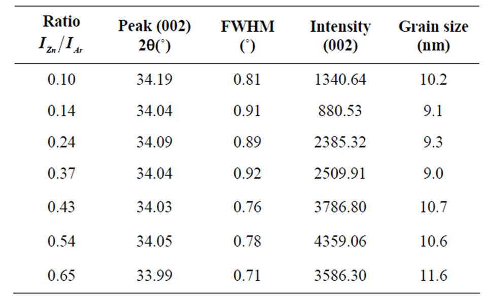
Table 2. Measurements of the peak (002) angle, FWHM, intensity and grain size.
 (a)
(a) (b)
(b)
Figure 4. (a) XRD spectra of ZnO films deposited in plasmas with different intensity ratios . (b) Graph of the ratio between the surface roughness and thickness as a function of the growth rate of the oxidized region.
rate of 5 nm/min. In our study, for the film with intensity  = 0.10, with a growth rate of ~ 5 nm/min, the same exponent β as that found previously [13] was obtained. Thus, for the films with intensities
  > 0.10, we observe that the exponent β < 0.76.
4. Conclusion
In this study we investigated the effect of the rate of sputtering on ZnO thin films. The films were deposited onto glass substrates by RF magnetron sputtering. The results show that the films have an optical transmittance greater than 80% for wavelengths between 450 and 650 nm. However, with the increase in the sputtering rate, the absorption edge became greater than 427 nm. The optical gap of ZnO was (3.28 ± 0.01) eV. All the films were polycrystalline with a hexagonal wurtzite ZnO structure and grew preferentially along the c-axis of the crystal lattice. For the stoichiometric deposition zone, the morphological evolution of the films became slower for  of more than 0.10. For the film deposited at
  = 0.10, the growth exponent β = 0.76. For films grown at higher intensity ratios, the surface texture evolved later. This indicates that the greater density of Zn atoms promotes surface diffusion during film growth.
5. Acknowledgements
The financial support of the Brazilian agencies FAPESP (Proc. # 2008/53311-5 and # 2011/21345-0) and CNPq is gratefully acknowledged.
REFERENCES
- S. Lee, S. Bang, J. Park, S. Park, W. Jeong and H. Jeon, “The Effect of Oxygen Remote Plasma Treatment on ZnO TFTs Fabricated by Atomic Layer Deposition,” Physica Status Solidi, Vol. 207, No. 8, 2010, pp. 1845- 1849. http://dx.doi.org/10.1002/pssa.200925514
- M. Jiang, X. Liu and H. Wang, “Conductive and Transparent Bi-Doped ZnO Thin Films Prepared by rf Magnetron Sputtering,” Surface and Coatings Technology, Vol. 203, No. 24, 2009, pp. 3750-3753. http://dx.doi.org/10.1016/j.surfcoat.2009.06.014
- Y. Nakanish, A. Miyake, H. Kominami, T. Aoki, Y. Hatanaka and G. Shimaoka, “Preparation of ZnO Thin Films for High-Resolution Field Emission Display by Electron Beam Evaporation,” Applied Surface Science, Vol. 142, No. 1, 1999, pp. 233-236. http://dx.doi.org/10.1016/S0169-4332(98)00654-0
- B. J. Jin, H. S. Woo, S. Im, S. H. Bae and S. Y. Lee, “Relationship between Photoluminescence and Electrical Properties of ZnO Thin Fillms Grown by Pulsed Laser Deposition,” Applied Surface Science, Vol. 521, 2001, pp. 169-170.
- A. B. Djurišić and Y. H. Leung, “Optical Properties of ZnO Nanostructures,” Small, Vol. 2. No. 8-9, 2006, pp. 944-961. http://dx.doi.org/10.1002/smll.200600134
- F. Siah, Z. Yang, Z. K. Tang, G. K. L. Wong, M. Kawasaki, A. Ohtomo and Y. Segawa, “In-Plane Anisotropic Strain of ZnO Closely Packed Microcrystallites Grown on Tilted (0001) Sapphire,” Journal of Applied Physics, Vol. 88, No. 5, 2000, pp. 2480-2483. http://dx.doi.org/10.1063/1.1287527
- Y. P. Liao, J. H. Zhang, S. X. Li, Z. S. Guo, J. Cao, W. Q. Zhu and X. Li, “Structural Evolution of ZnO Films Deposited by rf Magnetron Sputtering on Glass Substrate,” Physica Status Solidi A, Vol. 207, No. 8, 2010, pp. 1850- 1853. http://dx.doi.org/10.1002/pssa.200925131
- J. G. Lu, Z. Z. Ye, Y. J. Zeng, L. P. Zhu and L. Wang, “Structural, Optical, and Electrical Properties of (Zn,Al)O Films over a Wide Range of Compositions,” Journal of Applied Physics, Vol. 100, No. 7, 2006, Article ID: 073 714. http://dx.doi.org/10.1063/1.2357638
- P. D. Nsimama, G. A. Niklasson, M. E. Samiji, G. W. Mbise and J. Wennerberg, “Plasma Emission Monitoring (PEM) Controlled DC Reactive Sputtered ZnO:Al Thin Films,” Vacuum, Vol. 86, No. 12, 2012, pp. 1939-1944. http://dx.doi.org/10.1016/j.vacuum.2012.03.052
- S. F. Szymanski, M. T. Seman and C. A. Wolden, “Plasma and Gas-Phase Characterization of a Pulsed Plasma-Enhanced Chemical Vapor Deposition System Engineered for Self-Limiting Growth of Aluminum Oxide Thin Films,” Surface and Coatings Technology, Vol. 201, 2007, pp. 8991-8997. http://dx.doi.org/10.1016/j.surfcoat.2007.04.076
- T. Wallendorf, S. Marke, C. May and J. Strumpfel, “Optical Investigations in a PEM Controlled Reactive Magnetron Sputter Process for Aluminium Doped Zinc Oxide Layers Using Metallic Alloy Targets,” Surface and Coatings Technology, Vol. 174-175, 2003, pp. 222-228. http://dx.doi.org/10.1016/S0257-8972(03)00696-0
- K. Ellmer, A. Klein and B. Rech (Eds.), “Transparent Conductive Zinc Oxide: Basics and Applications in Thin Film,” Springer, New York, 2008. http://dx.doi.org/10.1007/978-3-540-73612-7
- A. M. Rosa, E. P. Silva, M. Chaves, A. C. Catto, P. N. Lisboa-Filho and J. R. R. Bortoleto, “Growth Evolution of ZnO Thin Films Deposited by RF Magnetron Sputtering,” Journal of Physics: Conference Series, Vol. 307, No. 1, 2012, Article ID: 012020. http://dx.doi.org/10.1088/1742-6596/370/1/012020
NOTES
*Corresponding author.