Materials Sciences and Applications
Vol. 4 No. 6 (2013) , Article ID: 33476 , 20 pages DOI:10.4236/msa.2013.46049
Detailed Analysis of Five Aspects Addressed to Minimize Costs and Waste in the Chemical Bath Deposition of CdS Films Using the CdB–AC6H5O7–AOH–(NH2)2CS System
![]()
Departamento de Investigación en Polímeros y Materiales (DIPM), Universidad de Sonora, Calle Rosales y Blvd. Luis Encinas S/N, Col. Centro, C.P. 83000, Hermosillo, Sonora, Mexico.
Email: jgarciavlz@gmail.com, omarcastelo@correoa.uson.mx, mrbaezg@gmail.com, msotelo@guaymas.uson.mx
Copyright © 2013 J. A. García-Valenzuela et al. This is an open access article distributed under the Creative Commons Attribution License, which permits unrestricted use, distribution, and reproduction in any medium, provided the original work is properly cited.
Received December 15th, 2012; revised March 26th, 2013; accepted April 11th, 2013
Keywords: Thin Films; Cadmium Sulfide; Chemical Bath Deposition; Economization; Environmental Friendliness
ABSTRACT
Five studies were conducted in order to produce less waste and economize the application of a CdCl2–Na3C6H5O7– KOH–H3BO3/NaOH/KCl–(NH2)2CS definite aqueous system in the chemical bath deposition of CdS thin films, as well as to generate supporting information helpful to explain the effects of varying certain parameters established for the use of this formulation. These studies are related to the utility of the pH 10 borate buffer, to the selection of the appropriate OH– concentration, commercial alkali, and reaction temperature, and to the reusing of the residual solution. These studies were conducted by means of optical characterization, pH measurements, energy consumption tests, and chemical analysis; and all possible implications were analyzed in detail and widely supported by the literature. It is observed that the addition of 5.0 mL of pH 10 borate buffer in the reaction solutions only causes a slight reduction in the pH value and, therefore, in the thickness of the resulted films. It is observed that a decrease in CdCl2 concentration causes an increase in the pH values, and when such reagent concentration is varied it is necessary to determine the pH value at which the best CdS films can be obtained; this indicates the existence of an optimum pH of deposition, depending on the used reagent concentrations. It is demonstrated that the use of KOH and NaOH is interchangeable, and the advantages of NaOH are evaluated in the context of hygroscopicity, CO2 absorption, purity, and price. It is observed that the energy consumption when depositing a determined film is lower at high temperatures, and it is concluded that the time and energy savings at high temperatures are undoubtedly advantages in the deposition process of CdS thin films. A formulation to recycle the residual solution is presented, which is very important for the reducing of residual volume, and, therefore, in the minimizing of the environmental impact. An indirect objective of this work is to generate interest in identifying those points that could be modified in other chemical formulations to minimize costs and waste.
1. Introduction
Certainly, the main objective of the research groups focused on the development of photovoltaic devices, such as solar cells, is the fabrication of a product that achieves the maximum conversion efficiency. After an analysis of the literature, our working group concluded that, in addition to the conversion efficiency, the product becomes more valuable when the fabrication of the device is supported on the minimization of overall costs and the environmental friendliness. This means that several aspects related to the production of the constituent materials of such devices have to be modified. Therefore, we consider that the first steps to comply with the two raised points involve the following: a) the use of rapid, simple operation, and minimum energy consumption techniques; b) the use of inexpensive and accessible raw materials, and the achievement of their maximum use; and c) the use of low-toxicity reagents, combined with a lower production of waste. Of course, these actions should not affect, at least not to a large extent, the functional properties of the constituent materials of the devices of interest.
Although the interest by the scientific community in the environmental friendliness and the minimization of overall costs was apparently relegated to second place, there are some publications—which will be referred to in the following sections—in which the authors have considered some issues related to the arguments mentioned in the previous paragraph. This is precisely which has motivated us to address the issues of the costs and environmental impact resulting from the process of synthesis of cadmium-sulfide (CdS) thin films, which is a semiconductor material that acquired interest from the scientific community—interest that has remained strong to date of publication of this work—due to the photovoltaic effect observed by Reynolds et al. during the course of their investigation with the photoconduction and rectifycation properties of CdS crystals, which was reported in 1954 [1], and to the possibility of fabricating photovoltaic cells from polycrystalline CdS films, as studied and demonstrated by Carlson et al. in their work reported in 1956 [2] and in that patented in 1958 [3]. In this regard, we concluded that further research is required to improve the application or use of the techniques and methods— even the selection of raw materials—that have made great strides in reducing the environmental impact of waste produced, without adversely affecting the costs of synthesis or the CdS properties.
Among the techniques for the synthesis of thin films, it is well-known that the chemical bath deposition is a flexible, inexpensive, effective, and experimentally simple technique for the synthesis of semiconductor thin films in laboratory conditions [4], and it is probably the simplest available technique for such purpose [5]. The earliest work reporting on the application of the chemical bath deposition technique for the synthesis of CdS thin films is credited to Mokrushin and Tkachev, with their work reported in 1961 [6], although CdS deposited from a thiosulfate ( ) solution was already noted by Allen et al. in 1912 [7]. Anyway, with the work of Mokrushin and Tkachev [6] a standard aqueous reaction system consisting of three components was established: a cadmium-salt (CdB) as Cd2+ ions source, thiourea ((NH2)2CS) as S2– ions source, and ammonium-hydroxide (NH4OH) as OH– ions source, which, in the ammonia (NH3) form, also acts as a Cd2+ ions ligand.
This CdB–H2O-NH3– -OH––(NH2)2CS aqueous system, which may contain an ammonium-salt (NH4B) to buffer the solution, remained basically unchanged in the studies reported by several authors during the following two decades [8-13]. The first modifications to this standard system were made by Call et al. in 1980 [14], who used cyanide (CN–) as ligand instead of NH3, and by Mondal et al. in 1983 [15] and Bhardwaj et al. in 1984 [16], who introduced triethanolamine (N(CH2CH2OH)3) as ligand besides NH3. The use of N(CH2CH2OH)3 was taken by the group of Nair and Nair, who reported several works using this ligand [17-27]. But in 1994 they reported [28] a formulation in which citrate (
 ) was used as ligand instead of N(CH2CH2OH)3, besides including NH3. This change was originated from the use of
  in the chemical bath deposition of cadmium-selenide (CdSe) thin films in a work reported one year earlier [29].
This citrate–ammonia-containing formulation [28,30- 33] was later studied by the group made up by Ramí- rez-Bon, Sotelo-Lerma, and collaborators, who also designed a modification, which was first used in a work of Castillo et al. in 1998 [34] and first described by Orozco-Terán et al. one year later [35]. This modification consisted, basically, in the establishment of the use of cadmium-chloride (CdCl2) as Cd2+ ions source, and in the use of potassium-hydroxide (KOH) and pH 10 ammonia buffer—composed of ammonium-chloride (NH4Cl) and NH4OH—instead of only NH4OH. This modification was based on some observations derived from the synthesis of CdS in zeolites [36] and from the experience acquired [37-40] with the use of the ammonia-containing formulation employed by the group made up by Zelaya-Angel and collaborators [37-51], which basically differs from the standard chemical formulation employed by Nagao and Watanabe [10] in the use of CdCl2 instead of cadmium-nitrate (Cd(NO3)2).
However, it was not until the report of Ortuño-López et al. in 2002 [52] when the use of NH3/ was completely removed from this citrate-containing formulation by replacing the pH 10 ammonia buffer with pH 10 borate buffer—composed of boric-acid (H3BO3), sodiumhydroxide (NaOH), and potassium-chloride (KCl)—, which was justified in terms of environmental friendliness one year later [53]; thus resulting in the CdCl2– Na3C6H5O7–KOH–H3BO3/NaOH/KCl–(NH2)2CS definite system—in which the pH 10 borate buffer is included or not—which since this moment was labeled as ammonia-free system—although this label had been already used by Němec et al. in 2002 [54,55] for a system containing nitrilotriacetate (
 ) as ligand. In addition, in 2004 Ortuño-López et al. reported another work [56] in which they succeeded in obtaining of CdS thin films using low concentrations of all the reagents, being able to use even the half of the concentrations used in the original ammonia-free citrate-containing formulation. Then, although with small variations in the concentrations of the reagents, this less-harmful formulation began to be widely used by research groups in Mexico and USA [4,56-71], and in other countries [72-74].
It is important to highlight these small variations in the concentrations of the reagents often applied to this latter ammonia-free citrate-containing formulation, since the reports in which these variations were applied, although in some cases do mention the effect of this action on the properties of CdS films, do not include a solid argument to justify the application of such variations and to explain their effects. For environmental reasons we decided to perform our researches by using this less-harmful formulation, and in this work we decided to conduct studies—not only about the concentration of reagents—in order to experimentally support the changes that can be made to this formulation, all this in the context of economize its application and generate less waste. Henceforth, this less-harmful chemical formulation will be appointed as Ortuño-López–2004 formulation—see Table 1.
The studies to be performed are:
1) An investigation about the effect of adding the pH 10 borate buffer on the pH of the reaction solutions and the optical properties of the resulting CdS thin films.
2) Various tests, at a defined Cd2+ concentration, to determine the OH– concentration with which a better adherence and wider interval of thickness can be obtained.
3) An investigation about the effect of using NaOH instead of KOH as source of OH– ions.
4) An investigation for determine the best reaction temperature that permits energy saving.
5) Various experiments to deposit thin films by using a reaction solution prepared from the residual solution after the first deposition reaction.
This work, by means of all these experiments, aims to generate interest in identifying those points that could be modified in other chemical formulations to minimize costs and waste, and generate information to chemically understand the effects of these modifications. For such purpose, all the experimentally studied issues presented in this work are analyzed in detail, and all the discussions are widely supported by the literature. For a better presentation of this paper, the results and discussion section is divided into five subsections, which begin with a brief background about the issue to be addressed.
2. Experimental Details
Reaction solutions with different concentrations were prepared for the CdS thin film synthesis in a 100-mL beaker by using the following stock reagent solutions: 0.05 M CdCl2 (Spectrum, 95.0% purity), 0.50 M sodiumcitrate (Na3C6H5O7·2H2O, Fermont, 99.7% purity), 0.50 M KOH (J.T. Baker, 87.6% purity), 0.50 M NaOH (J.T. Baker, 98.6% purity), 0.50 M (NH2)2CS (Fermont, 99.9% purity), and pH 10.01 borate buffer (J.T. Baker). Corning float glass microscope slides were used as substrates, which were washed with water and liquid soap and dried with a hair dryer prior to deposition reaction. The substrates were immersed in the reaction solution within 5 to 20 s after its preparation; thus, the difference between immersion time and reaction time is negligible compared to the duration of the studied reaction times and, therefore, immersion time and reaction time will be considered identical. Unless a different temperature is specified, the deposition reactions were done at 70˚C by submerging the 100-mL beaker containing the reaction solution and the substrates in a water bath inside a Lauda Ecoline Staredition RE 106 refrigerating bath/circulator, E 100 controller, with a chamber capacity of 6 L.
The substrates covered with CdS film were sequentially withdrawn from the reaction solution at different immersion times. At the end of each immersion time, the withdrawn substrates covered with CdS film were rinsed with distilled water, and the non-adhered precipitates on the film surface were removed using damp cotton and more distilled water. Then, the samples were dried in the air. The chemical formulation and the type of substrates employed here only allow adherence of the CdS thin films to the tin side of the substrates, however, in those cases in which CdS films were adhered to the non-tin side of the float glass substrate, the films were removed by using a cotton swab moistened with dilute hydrochloric-acid (HCl), and then the samples were rinsed with distilled water and dried in the air again.
A Dynatech Nevada Inc. 235A safety/ECG analyzer was used to determine the energy consumption of the electrical equipment containing the water bath. The pH
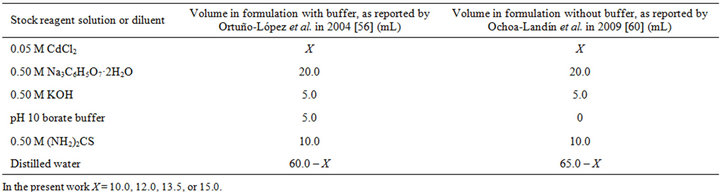
Table 1. Formulations for the chemical bath deposition of CdS thin films using pH 10 borate buffer, as studied by Ortuño-López et al. [56], and not using pH 10 borate buffer, as studied by Ochoa-Landín et al. [60].
of the reaction solutions was measured by using a Hanna Instruments HI 2212 flexible calibration pH meter equipped with a Hanna Instruments HI 1131B combination pH electrode. The glass electrode was calibrated against standard pH 7.00, pH 4.01, and pH 10.01 buffers. For the study of the optical properties, the absorbance, A, of the samples was measured at an interval of wavelength, λ, from 300 to 1100 nm in the near-ultraviolet/visible/ near-infrared (NUV/Vis/NIR) spectrum using a Perkin Elmer UV-Vis Spectrometer Lambda 20 instrument. To measure A in the case of reaction solutions, a solution containing all the reagents, except the analyte, was used as the blank. In the measurement of thin films a Corning float glass slide was used as the blank. In this case, A will be referred to as the logarithm of the inverse of optical transmittance, log(T –1), since optical specular reflectance, R, was not measured. Under certain conditions, the log(T–1) value is proportional to the thin film thickness, d, and the absorption coefficient, α, by the following relation [75]:
 , (1)
, (1)
which can be reordered to include the term of interest:
 . (2)
. (2)
As will be seen in the spectra presented in the following sections, the increase in log(T –1) value with increasing reaction time, which naturally increases d, occurs at λ shorter than about 450 nm and longer than about 800 nm. Therefore, in this study the log(T –1) value at 400 nm will be used as a rough indication of the thin film d; the main aim of the use of this arbitrarily chosen λ, based on the latter, is to know the film growth tendency. The chemical bonding of the CdS thin films was analyzed by X-ray photoelectron spectroscopy (XPS) using a Perkin-Elmer Physical Electronics PHI 5100 spectrometer equipped with a non-monochromatic Mg Kα X-ray source (1256 eV) and a hemispherical analyzer.
As safety precautions, before starting the experimental reproduction of this work, we recommend to read the indications described in the material safety data sheets of all reagents used here, including for hydrogen-sulfide (H2S), which is produced by the reaction between CdS and HCl, and take the pertinent precautions. Also ensure that the generated residues will be treated or confined.
3. Results and Discussion
3.1. Omission of the pH 10 Borate Buffer
As mentioned in the introduction of this paper, the use of a pH 10 buffer in the Ortuño-López–2004 formulation is based on the observations derived from the synthesis of CdS in zeolites [36] and from the experience acquired [37-40] with the use of the standard formulation employed by the group made up by Zelaya-Angel and collaborators [37-51]. Although it is thought that the purpose of the addition of pH 10 buffer in this formulation is to regulate the pH of the reaction solution throughout the course of the deposition reaction, there are no reports that demonstrate this assumption. In fact, the volume reported of pH 10 buffer—specifically a pH 10 borate buffer— added to the reaction solution, whose final volume is 100.0 mL, was decreased from 20.0 [52] to 5.0 mL [53] with no observed adverse results. On the other hand, it is well-known that the buffer capacity depends on the total concentrations of the chemical species that have this buffering effects [76], which greatly decreases when a dilution as drastic as 1:20 is performed, which is obtained by diluting 5 mL of buffer to a final volume of 100 mL, as done in the Ortuño-López–2004 formulation. This suggests that the omission of the pH 10 borate buffer does not affect the properties of CdS films. However, it is necessary to determine the true effect of the addition of pH 10 buffer to the reaction solution.
To date, the only work that provides information about the effect of adding 5.0 mL of pH 10 borate buffer in the Ortuño-López–2004 formulation is that reported by Ochoa-Landín et al. in 2009 [60]. They synthesized four sets of CdS thin films within the parameters of temperature, reagent concentration, and immersion time that were used in the work reported by Ortuño-López et al. [56], but with the difference that no buffer was added to the reaction solutions. Then, they compared their results with those reported by Ortuño-López et al. five years ago [56], finding only minor differences, which provided arguments for their discussion. A critical comparison between the two mentioned publications clarifies the high similarity of the general properties of CdS thin films deposited with and without pH 10 borate buffer, despite that they were made by different persons and probably with different batch reagents, but maintaining unchanged the rest of the conditions specified in the OrtuñoLópez–2004 formulation. At first sight, this is indicative of the high reproducibility of using this formulation, even with the addition of certain chemicals.
However, aimed to confirming the existence of those minor differences in the properties of the CdS thin films deposited from reaction solutions containing and not containing pH 10 borate buffer, and, if such minor differences exists, to determine their causes, we proceeded to repeat the synthesis of CdS thin films reported in both publications under the same working conditions and using the same stock reagent solutions for all the deposition reactions. This consisted of four sets of CdS films, for whose synthesis the volume of 0.05 M CdCl2 was varied —in this case by using 10.0, 12.0, 13.5, and 15.0 mL— according to the specifications described in Table 1. The log(T –1) spectra of the resulted CdS thin films deposited during 15 min of reaction are shown in Figure 1, whose analysis is discussed in the following paragraphs.
Several observations resulted from varying the CdCl2 volume and from the use or omission of the pH 10 borate buffer. First, the thin films were destroyed with the damp cotton when 10.0 mL of 0.05 M CdCl2 was used regardless of adding the pH 10 buffer or of the studied immersion time. Second, when 12.0 mL of CdCl2 was used the thin films were destroyed with the damp cotton at immersion times greater than 20 min, regardless of the addition of the pH 10 buffer. Third, as the amount of CdCl2 was increased, maintaining constant the immersion time, the log(T –1) values also increased. According with that discussed with Equation (2), this is directly related to the increase in thin film d. This increase in the growth rate by increasing the Cd2+ ions amount is widely supported by the literature [56,60,77-86]. Fourth, as reported by Ochoa-Landín et al. [60], there is a slight difference between the films deposited in a reaction solution containing pH 10 borate buffer, compared with those deposited in the absence of the buffer. In our experience, that small difference between films obtained in two different deposition runs usually results from slight errors in the measurement of the reagent volumes used for the preparation of the reaction solutions; however, this experiment was repeated several times and always resulted in the same tendency. Therefore, this small difference in the log(T –1) spectra due to a slight decrease in the d—according to Equation (2)—of the films deposited in the presence of the pH 10 buffer, for each immersion time and CdCl2 concentration, is definitely an effect of the addition of the
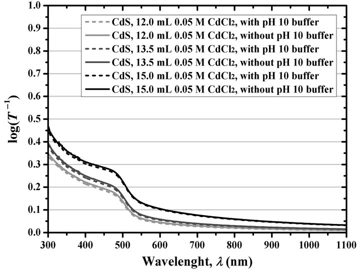
Figure 1. Variation of the logarithm of the inverse of optical transmittance of CdS films deposited at 15 min with different 0.05 M CdCl2 volumes, by using the Ortuño-López– 2004 formulation with and without pH 10 borate buffer.
buffer. One parameter that has not been considered up to this point, and a very important one that also affects the growth rate of the CdS thin films and that could explain the foregoing is the pH of the reaction solutions, whose effect on the growth rate of CdS thin films—or in the precipitation rate of CdS—has been noted by several authors [54,78-81,87-89].
To corroborate if the pH of the reaction solutions with and without pH 10 borate buffer is responsible for the small differences in the d of deposited films, we measured the pH of each reaction solution used in the present study, and the results are shown in Figure 2. A very important observation resulting from this measurement is that the pH values of all the reaction solutions are always higher than 12. This means that the addition of a defined volume of pH 10 buffer naturally will cause a decrease in the pH of the reaction solution, as shown in the figure, in which all the pH values of solutions prepared with the pH 10 borate buffer were lower than those of the solutions prepared without the buffer, for each CdCl2 concentration measured. This study revealed a decrease of about 0.03 pH units—at pH values around 12—when 5.0 mL of the pH 10 borate buffer was added to the reaction solutions, this being the cause of the slight decrease in growth rate of the thin films deposited in the presence of the buffer. Furthermore, due to the high pH values of the reaction solutions, the buffer capacity of the pH 10 borate buffer, efficient at pH 10, is completely lost, and its addition to the reaction solutions only causes the mentioned slight decrease in the pH values. Moreover, the addition of the pH 10 borate buffer creates the possibility of doping the resulting CdS thin films with boron atoms, according to the discussed in the reports of several authors who used H3BO3 for doping CdS [90-97].
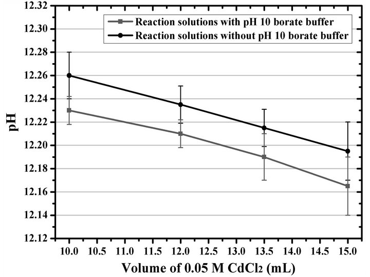
Figure 2. Variation of the pH of the reaction solutions prepared by means of the Ortuño-López–2004 formulation with and without pH 10 borate buffer as a function of the 0.05 M CdCl2 volume.
On the other hand, simply decreasing in about 0.20 mL the volume of KOH in those solutions without the pH 10 buffer is enough to match the pH values of the solutions with and without the buffer—or otherwise, by increasing about 0.20 mL the volume of KOH in the solutions with the buffer. This leads to similar films for both cases, which shows that it is not necessary to add a volume of pH 10 borate buffer to the studied CdCl2–Na3C6H5O7– KOH–(NH2)2CS definite system. Moreover, eliminating the use of the pH 10 borate buffer allows reagent saving and reduction of processes. However, the possibility of testing the buffer efficiency of some systems at pH values around 12 is not discarded, or, even, to test whether such buffering is really necessary.
3.2. Selection of an Appropriate pH
An important aspect of Figure 2 is that an increase in 0.05 M CdCl2 volume leads to a decrease in the pH values of the reaction solutions. This is understood when considering the interaction between Cd2+ ions or cadmium–citrate complexes and OH– ions, according to the following general equation:
 (3)
(3)
In accordance with this equation, by increasing the CdCl2 amount and keeping constant the KOH amount the reaction is displaced to the right, to the formation of the [Cd(C6H5O7)b(OH)h(H2O)6 – 3b – h]2 – 3b – h species with subsequent reduction of free OH– ions, according to the principle of Le Châtelier. Therefore, when maintaining constant the concentration of the other reagents, it is clear that a decrease in the CdCl2 concentration results in an increase of the pH value of the reaction solution. This could alter the delicate chemical species distribution that gives rise to compact and good quality CdS films. This means that, when the CdCl2 concentration is varied, a pH adjustment is necessary, or even, a determination of the pH value at which the best CdS films can be obtained.
For example, our working group chose to perform the investigations by using a low concentration of CdCl2, in this case a Cd2+ concentration of 6 mM in the final reaction solution volume, obtained by using 12.0 mL of 0.05 M CdCl2 in 100.0 mL of reaction solution. As mentioned in the previous section, this CdCl2 concentration results in CdS films that are destroyed with the damp cotton after 20 min of immersion, an observation similar to that reported by Ortuño-López et al. [56] and Ochoa-Landín et al. [60] when they used 10.0 mL of 0.05 M CdCl2. To corroborate if the effect of a specific pH value of the reaction solution is the cause of this poor quality of the films, we synthesized and characterized four sets of CdS thin films in which, by using 12.0 mL of 0.05 M CdCl2 and no pH 10 borate buffer, the KOH concentration and the immersion time were varied, and the results are presented in Figure 3, in which it is first evident that the thin film growth rate increases by increasing the pH.
The figure shows that when using 5.0 mL of 0.50 M KOH, the maximum log(T–1) value at 400 nm and, therefore, the maximum d are obtained at 10 min of reaction, indicating a high deposition rate—apparently in a homogeneous precipitation tendency—that consumes the reactive chemical species at short immersion times. Also, this culminates with the destruction of the films with the damp cotton at immersion times greater than 20 min, as mentioned above. Something similar happens when using 4.0 mL of 0.50 M KOH, with the difference that the maximum d is obtained at 15 min and that no destruction occurs at any studied immersion time. The wider interval of d—wider interval of log(T –1) values—is obtained by using 3.0 and 2.0 mL of 0.50 M KOH, being higher when using 3.0 mL. A similar result when selecting a specific immersion time value, but greater than 15 min with the aim to compare with our case, was noticed by Němec et al. [54] and Khallaf et al. [89] for nitrilotriacetate-containing aqueous systems.
For this reason, we selected 3.0 mL of 0.50 M KOH as the most appropriate volume for the synthesis of CdS thin films when 12.0 mL of 0.05 M CdCl2 is used maintaining constant the other reagents, which leads to a pH equal to 11.92. When using more than 3 mL of KOH the maximum d is getting smaller, although it is reached at immersion times increasingly lower. From this study it is clear that there is an optimum pH value of deposition for each concentration of reagents. Furthermore, this opens the possibility to use even lower amounts of CdCl2—even lower than 10 mL, which is the minimum value studied by Ortuño-López et al. [56] and Ochoa-Landín et al. [60]—to obtain CdS thin films once the optimum pH of synthesis for the selected Cd2+ concentration has been determined. Besides the reduction in the costs of raw materials, this allows the reduction of toxic material concentration in the reaction residues.
3.3. Use of NaOH Instead of KOH
Another important aspect for the reduction of costs in the area of raw materials used for the synthesis of CdS thin films is the implementation of the use of reagents that are inexpensive and generate higher yields. A clear example of this is the substitution of KOH, the commonly used alkali, by NaOH, which is a more advantageous reagent. The most relevant subjects that were considered for this
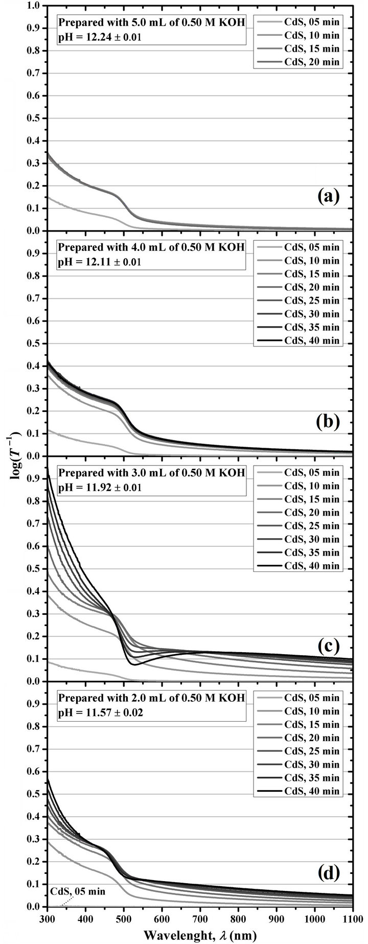
Figure 3. Logarithm of the inverse of optical transmittance of the CdS thin films deposited at different immersion times by using 100.0 mL of reaction solution prepared with 12.0 mL of 0.05 M CdCl2, 20.0 mL of 0.50 M Na3C6H5O7, Y mL of 0.50 M KOH, 10.0 mL of 0.50 M (NH2)2CS, and water; where Y is equal to (a) 5.0, (b) 4.0, (c) 3.0, and (d) 2.0.
comparison are the hygroscopicity and absorption of carbon dioxide (CO2) from the environment, and the purity and price of the commercial presentations.
In the cases of water and CO2 absorption, it is wellknown that KOH is more hygroscopic than NaOH—in fact, KOH is a desiccant of greater intensity than NaOH [98]—and it is a better absorber of CO2 compared with the absorbing capacity shown by NaOH [99]. Also, there are some reports that showed that KOH aqueous solutions are better CO2 absorbers than NaOH aqueous solutions [100-102]. For reagent solution preparation and storage purposes, these aspects are a disadvantage of KOH, since to prevent rapid loss of purity due to the absorption of water and the formation of carbonate ( ) as a consequence of absorption of CO2 [101], its handling requires more care compared with NaOH. This is not a justification for neglecting the preparation and storage processes of NaOH solutions. Although the NaOH solutions require less care, we recommend a quick preparation of the NaOH solutions—and the same for KOH solutions—in a low humidity and low CO2 environment, a subsequent titration of the solutions to corroborate the molarity, and their storage in a sealed plastic container.
On the other hand, when considering the prices for bottles with 500 g of product—pellets, reagent, ACS— taking as an example the Spectrum reagent brand, through its 2013 website, the NaOH bottle is more economical, with a price of US$ 70.00, whereas the KOH one has a price of US$ 77.90; that is, 500-g bottles of commercial NaOH are 10.14% cheaper than KOH ones. However, two more important considerations than the product bottle price is the purity of the commercial material and the molar mass of the compound, since NaOH, besides having a lower molar mass, is commonly obtained with a purity of about 97.0%, whereas KOH is obtained with about 85.0% purity. This means that a 500-g bottle of commercial NaOH contains 12.125 mol of OH– ions, whereas 500-g bottle of commercial KOH only contains 7.576 mol of OH– ions. In conclusion, taking into account molar mass of the compounds and price and purity of the commercial materials, the price of each mole of KOH is US$ 10.28, whereas the price of each mole of NaOH is only US$ 5.77—see Table 2. This means a monetary saving of 43.9% in cash destined to the OH– source reagent when using NaOH instead of KOH, which becomes very important in the industrial scale production of CdS.
Definitely, it is more convenient the use of NaOH than KOH. However, to confirm if their use is interchangeable, we deposited CdS thin films at different immersion times by using 3.0 mL of each 0.50 M alkali, 12.0 mL of 0.05 M CdCl2, and no pH 10 borate buffer, resulting in
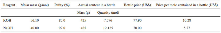
Table 2. Main details of commercial KOH and NaOH for 500-g bottle presentations.
slight differences—much smaller than those caused by the addition of pH 10 buffer—between the films deposited in both cases, for each immersion time, as shown in Figure 4. These slight differences, mainly at long immersion times, are due to minuscule experimental errors in the preparation of the stock reagent solutions, specially for the hygroscopic KOH reagent, and in the measurement of the reagent volumes used for the preparation of the reaction solution, as well as the arrangement of the substrates in the reaction beaker, as we noticed experimentally. With this study, the economic advantage in reducing reagent costs as well as process costs is clear when NaOH is used instead of KOH.
Due to the omission of the pH 10 borate buffer, the use of minimum amounts of Cd2+ and OH– ions, and the advantages of using NaOH instead of KOH, the resulting chemical formulation becomes more economical and less harmful. Mainly for the economical reason, from this point on we will refer to it as economical formulation—although this can be further enhanced—whose specifications are depicted in Table 3. These specifications can be changed—usually a variation in the Cd2+ concentration is done—but it is necessary to take into account that the deposition conditions, like the pH of the

Figure 4. Logarithm of the inverse of optical transmittance of the CdS thin films deposited at different immersion times by using 100.0 mL of aqueous reaction solution prepared with 12.0 mL of 0.05 M CdCl2, 20.0 mL of 0.50 M Na3C6H5O7, 3.0 mL of 0.50 M alkali, either KOH or NaOH, 10.0 mL of 0.50 M (NH2)2CS, and water.
reaction solution, under which good quality films can be obtained, depending on the selected reagent concentrations, must be clearly identified.
3.4. Selection of a Convenient Temperature
One would think that the synthesis of CdS thin films at room temperature, or simply at low temperatures, is an advantage in the applying of a given chemical formulation in the deposition process. However, several authors have reported explicitly or implicitly that the lower the reaction temperature the lower the thin film growth rate [12,15,20,21,23,28,34,35,54,77-81,84,87,90,103-121].
Thus, without delving into the cases in which homogeneous precipitation is favored, which limits the maximum d—a limit which was directly reported [12,15,21] or simply evident in the results reported [115,118,120] by some authors—the use of low temperatures lengthens the time required to achieve a thin film with determined d compared to the time required at higher temperatures. For example, Figure 5 shows the log(T –1) value at 400 nm of the CdS thin films synthesized by using the economical formulation at different temperatures and different immersion times, and it confirms the increase in thin film growth rate with increasing temperature. This indicates that, for example, to achieve a log(T –1) value at 400 nm of 0.32, obtained during 160 min at 30˚C, an immersion time of 15 min at 70˚C is only required. This time saving when using high reaction temperatures is undoubtedly an advantage in the deposition process of CdS thin films.
On the other hand, although different authors have included in their reports studies in which the reaction

Table 3. Economical formulation for the synthesis of CdS thin films.
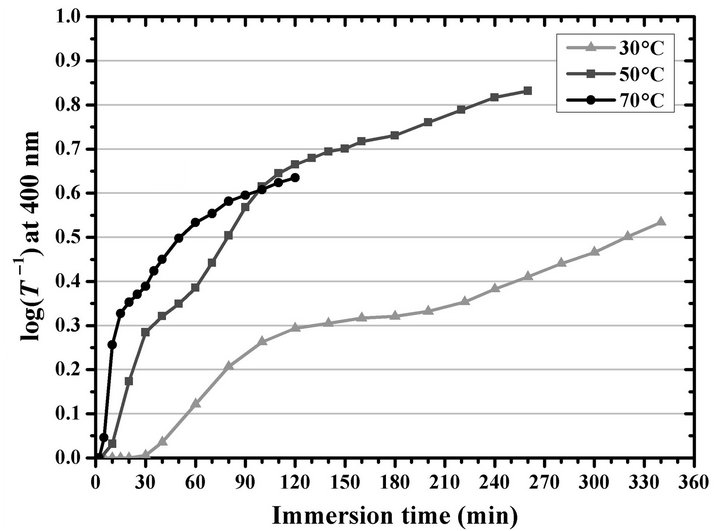
Figure 5. Logarithm of the inverse of optical transmittance at 400 nm of the CdS thin films deposited at different temperatures and immersion times by using the economical formulation.
temperature is varied [12,15,20-24,27,28,34,35,54,73, 77-81,84,85,87,89,90,103-132], there is no report about the energy consumption of the equipment that keeps constant the temperature of the water bath at a selected value. For this purpose, we measured the energy consumption during the first minutes when a temperature of 30˚C, 50˚C, and 70˚C is achieved, starting from a water bath at 25˚C. We observed that, as expected, the higher the temperature value to be reached the greater the time required to achieve it. Figure 6 shows the power, P, calculated by using the current, I, data recorded by the electrical safety analyzer from the moment at which the electrical equipment containing the water bath—connected to a 120-V line—was switched on until the moment when the selected temperature was stabilized. A P of about 1.36 kW was calculated during the heating mode until the water bath reached the selected temperature, which took about 1.3, 8.4, and 16.3 min to reach 30˚C, 50˚C, and 70˚C, respectively. Therefore, the higher the temperature to be reached the greater the energy consumed to achieve it. Furthermore, the continuous heating causes the system to reach about 0.4˚C above the selected temperature value, which activates the cooling mode, for which a P value between about 0.3 and 0.8 kW was recorded. Then, the energy consumption becomes progressively smaller until a stable temperature and stable P are achieved. From this moment, the water bath can be used for a reproducible deposition of thin films. The P from this point on was recorded with an average value of about 0.024, 0.060, and 0.132 kW, for temperatures of 30˚C, 50˚C, and 70˚C, respectively, with fluctuations that depend on the times at which the heating and cooling modes are activated.
The above means that reaching a higher temperature carries higher energy consumption. However, a method

Figure 6. Variation of the power calculated for the Lauda Ecoline Staredition RE 106 refrigerating bath/circulator as a function of the switched on time, taking into account the current recorded by the Dynatech Nevada Inc. 235A safety/ ECG analyzer to reach a temperature of (a) 30˚C, (b) 50˚C, and (c) 70˚C, starting from 25˚C.
could be designed to maximize the use of the hot water to avoid wasting the energy used for the heating. On the other hand, once the selected temperature is stabilized, the maintenance of a higher temperature also consumes more energy. At this point, however, to obtain a given d value, the total energy consumption is lower at higher temperatures. For example, to obtain a film with log(T –1) at 400 nm equal to 0.32 are required about 0.024 kW during 160 min at 30˚C, this is a total energy of 230.4 kJ; to obtain the same value of log(T –1) are required about 0.060 kW during 40 min at 50˚C, this is a total energy of 144.0 kJ; and for the case at 70˚C, are required about 0.132 kW during 15 min, this is a total energy consumption of 118.8 kJ. By considering that the total energy spent is lower at higher temperatures when the selected temperature is stabilized, in addition to the saving time, the use of high temperatures for deposition reactions definitely is more convenient.
3.5. Reutilization of Reaction Residues
In addition to production costs, it is also necessary to consider the costs resulting from the treatment of the chemical waste generated after the chemical bath deposition of CdS thin films. It is also very important to reduce the environmental impact of this chemical waste. Some aspects in reducing the environmental impact and the treatment costs of the generated chemical waste is the reduction of toxic compounds concentration—which has been dealt in previous sections—as well as of the residual volume.
A few authors have addressed some points related to these issues. For the case of a citrate–ammonia-containing system, the group of Nair and Nair conducted a mathematical model which can qualitatively account for most of the features of the experimental growth curves of the chemically deposited semiconductor thin films [84], a model that was used to study the thin film yield as a function of the separation among substrates in batch production, and they established that there is an optimum separation at which, for a given bath composition and temperature, about 90% of the maximum possible process yield is achieved [125]; based on this, they reported the achieving of a thin film yield of almost 100% for CdS with final d of about 50 nm by using very small substrate separation—0.1 mm—[133]. With the aim to improve yield and reduce waste in other ammonia-containing systems, Hariskos et al. synthesized CdS thin films by using fresh CdCl2 solutions and reusing the NH4OH and (NH2)2CS contained in the permeate separated from the waste after the deposition reaction [134], whereas Malinowska et al. implemented and described processes to recover and recycle NH4OH [135] and Cd2+ ions [136]. On the other hand, the group of O’Brien presented a process in which low Cd2+ ions concentration is used—achieved through the use of ethylenediamine (H2NCH2CH2NH2) as ligand instead of NH3—and a reaction system in which, among others aspects, the substrate is heated instead of the whole reaction solution in order to assist the heterogeneous precipitation, thus making more efficient the production of CdS films [137, 138]. The heating of the substrate was later used in a variation of the chemical bath deposition technique, which also utilizes a small volume of reaction solution, thus further increasing the efficiency of the reagents; this technique, described by McCandless and Shafarman [139,140] and used for the deposition of ultra-thin films, is called as chemical surface deposition [139-144]—with a slightly different arrangement, it has also been called as shallow chemical bath deposition [145,146]. All these and other approaches should be implemented or emulated to improve markedly the efficiency of a determined chemical formulation to deposit CdS thin films.
In a similar way to that reported by Hariskos et al. [134], we performed several experiments with the aim of determining the possibility of recycling the chemical residual solution generated from the deposition of CdS films by using the economical formulation. For this purpose, it was first necessary to identify which chemical reagents remain in the residual reaction solution and their concentration. Therefore, it is important to understand the reaction that occurs among all the reactants present in the reaction solution to give the CdS product, which can be summarized—by considering the formation of cyanamide (NH2CN) as a final product of the hydrolysis of (NH2)2CS [147]—by the following general equation:
 (4)
(4)
According to the above equation, Na3C6H5O7 is not consumed, since  acts as a Cd2+ ions ligand, which gradually releases Cd2+ ions during the course of the CdS formation reaction. Because of the used concentrations of reagents, which can be calculated from the data depicted in Table 3, the CdCl2 compound is the limiting reagent, thus, theoretically, its consumption must be completed, and, therefore, the consumption of (NH2)2CS should be proportional to the synthesized CdS. On the other hand, the reduction of OH– concentration, which is more complicated than the expressed in Equation (4) since NH2CN is hydrolyzed into products that apparently interact with OH– ions [147], can be known by a simple pH measurement with a glass electrode.
The simplest way to know the approximate amount of reagents consumed is by determining the portion of (NH2)2CS consumed after a deposition reaction. For this, we measured the intensity of the absorption peak at 236 nm at the beginning and at the end of the reaction—1 h of reaction. Figure 7 shows the result of this measurement, which was conducted after performing a dilution of 1:500 of the fresh and residual reaction solutions.
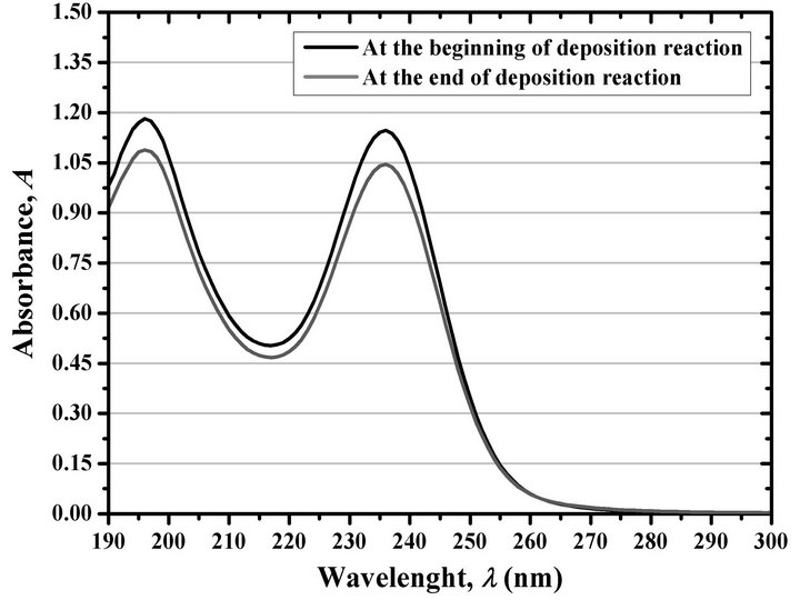
Figure 7. Absorbance of a reaction solution prepared according to the economical formulation at the beginning and the end of the deposition reaction, after a dilution of 1:500.
The observed decrease in A is due to a loss of about 9% of the amount of (NH2)2CS, indicating that a large amount of this compound remains in the residual reaction solution. Additionally, this 9% of (NH2)2CS almost coincides with the amount of Cd2+ present at the start of the reaction, which indicates a high consumption of the Cd2+ ions to form CdS.
By considering the above, we proceeded to take 90.0 mL of the residual solution, which is almost the 100% of the residual volume generated in one experiment conducted with the original fresh reagents. This volume of residual solution was obtained by filtering the final reaction solution, which, before filtering, was cooled during 1 h after finished the first deposition reaction. This residual solution contained, as determined experimentally, about 91% of the original (NH2)2CS, and, theoretically, 100% of the original Na3C6H5O7, besides remained OH– and Cd2+ ions and reaction byproducts. By using the residual solution, we replenished the consumed reagents for a second deposition reaction, but this was not enough to obtain compact and well adhered to the substrate CdS films, besides the thin film growth rate was decreased. As also observed by Hariskos et al. [134], the reaction byproducts apparently are responsible for the decrease of the thin film growth rate, impacting even—as we noticed and mentioned above—the quality and adhesion of the films. More research is required to identify the species responsible for this finding.
Due to the adverse results, we performed various tests by using 90.0 mL of the residual solution and different amounts for each stock reagent solution: 2.5 to 10.0 mL of 0.05 M CdCl2, 1.0 to 10.0 mL of 0.50 M (NH2)2CS, and 1.0 to 3.0 mL of 0.50 M NaOH. These amounts were varied not only to replenish the consumed reagents, but to find again the equilibrium among those chemical species that promote good quality CdS films, but now in the presence of the byproducts. The best CdS films were obtained when using the amounts specified in Table 4. The log(T –1) spectra of the films deposited during 20, 40, and 60 min of immersion by using these amounts is presented in Figure 8, which also shows the spectra for thin films deposited every 10 min during the first hour of reaction by using the original fresh reagent amounts of the economical formulation. The figure shows that the log(T –1) spectra of the thin films deposited during 40 and 60 min by employing the residual solution are almost identical, which indicates that the reaction finished at about 40 min. Furthermore, these spectra are compared only with the spectrum obtained just at 10 min by using fresh reagent solutions, besides the approximate λ where the log(T –1) begins to increase was displaced to shorter values. However, the results are acceptable because this process permits the recycling of the residual solution.
Moreover, Figure 9(a) and Figure 9(b) show the XPS results for the thin films deposited during 60 min for both conditions—prepared with fresh reagents and prepared with the residual solution. This study was conducted

Table 4. Formulation for a second CdS thin film deposition by reusing the residual solution.

Figure 8. Logarithm of the inverse of optical transmittance of CdS thin films deposited during 10, 20, 30, 40, 50, and 60 min by using fresh reagent solutions, according to the economical formulation, and during 20, 40, and 60 min by using the residual solution, according to the formulation for a second CdS thin film deposition.
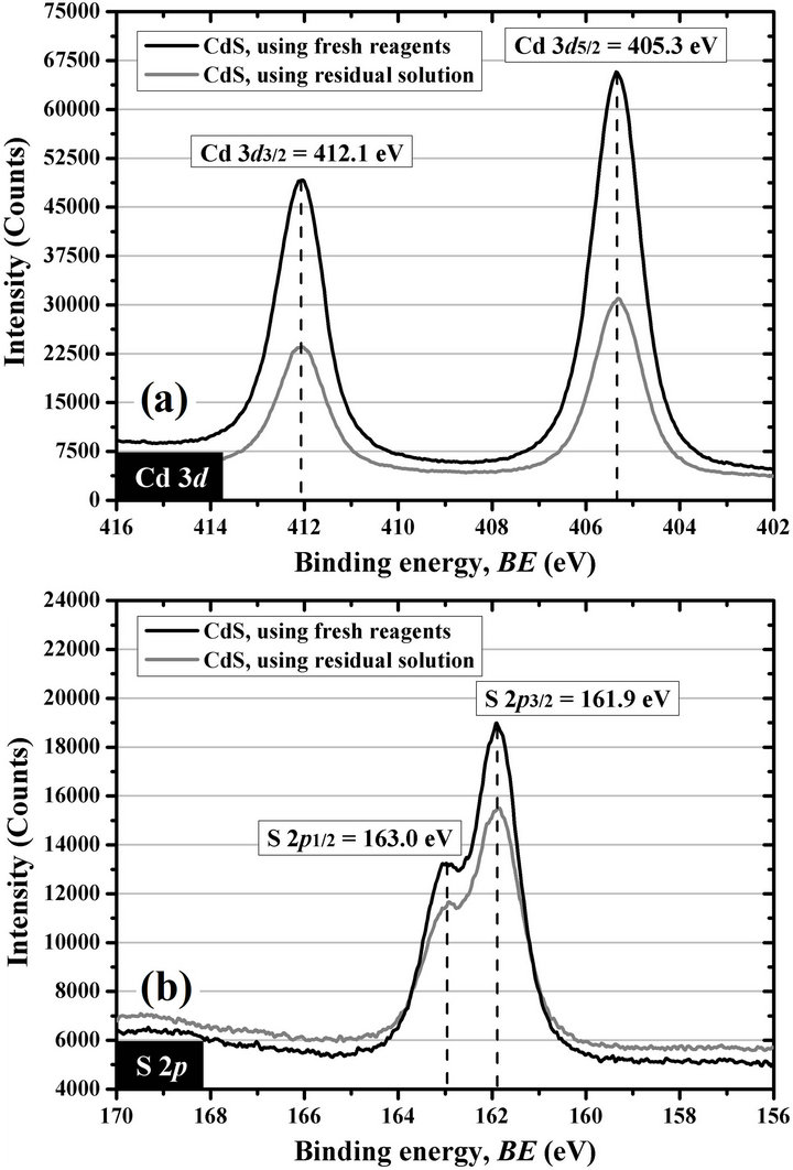
Figure 9. XPS spectrum of CdS thin films deposited during 1 h by using fresh reagent solutions, according to the economical formulation, and by using the residual reaction solution, according to the formulation for a second CdS thin film deposition, for (a) the Cd 3d region and (b) the S 2p region.
mainly to confirm if the thin films synthesized from the residual solution consist of CdS. As results, Figure 9(a) shows the location of the Cd 3d5/2 and Cd 3d3/2 peaks in 405.3 and 412.1 eV, respectively, whereas Figure 9(b) shows the S 2p3/2 peak in 161.9 eV and the S 2p1/2 peak in 163.0 eV, for both thin films. These peaks are very close to the location of the cadmium and sulfur signals reported by Mazón-Montijo et al. for CdS thin films synthesized in a first deposition reaction—reuse of residual solution not performed—under the same conditions, except that they were deposited on glass/indiumtin-oxide (glass/ITO) substrates at 4, 5, or 6 min of reaction, and by using 5.0 mL of 0.50 M KOH [64] instead of 3.0 mL of 0.50 M NaOH. This demonstrated the possibility of recycling the residual solution and thereby reducing the volume of waste produced during the chemical bath deposition of CdS thin films. However, more studies are still required to match the properties of the CdS thin films deposited by using the residual solution with those synthesized during the first deposition by using fresh reagent solutions.
4. Conclusions
Because the pH of a reaction solution prepared by using the Ortuño-López–2004 formulation is always higher than 12, the addition of a certain volume of pH 10 borate buffer will cause a reduction in that value. The slight difference in the pH values of the reaction solutions prepared with and without the 5.0 mL of pH 10 buffer results in slightly different thin film growth rates, and, hence, in slightly different d values when the thin films are deposited during the same immersion time using a defined Cd2+ concentration. The thin film d values can be matched when the initial pH values are equal. This means that the omission of the use of the pH 10 borate buffer in the Ortuño-López–2004 formulation does not cause adverse results.
Due to the existence of a chemical equilibrium between the cadmium-citrate complexes and cadmiumcitrate-hydroxo complexes, a decrease in the CdCl2 concentration causes an increase in the pH value of the reaction solution. This change in Cd2+ concentration and pH value could alter the delicate chemical species distribution that gives rise to good quality and well adhered to the substrate CdS thin films. Therefore, when the CdCl2 concentration is varied it is necessary to determine the pH value at which the best CdS thin films are obtained, which indicates the existence of an optimum pH of deposition depending on the used reagent concentrations.
It was demonstrated that the use of NaOH and KOH is interchangeable, since no optical differences were observed among the thin films deposited at the same immersion time and conditions, regardless of the used alkali. This reason, in addition to the lesser hygroscopicity, lesser CO2 absorption, higher purity, and lower price of the NaOH, is sufficient to justify the use of NaOH instead of KOH as OH– ions source.
When selecting a reaction temperature, it was observed that the higher the temperature to be reached the greater the time required to achieve it and, therefore, the greater the energy consumption. However, once the selected temperature is stabilized, it was observed that the total energy consumption to obtain a determined thin film d is lower at high temperatures. On the other hand, it was observed that the higher the temperature the higher the thin film growth rate and, therefore, the lower the time required to obtain a thin film with determined d. This time and energy savings at high temperatures are undoubtedly advantages in the deposition process of CdS thin films.
The reaction byproducts generated during the deposition reaction apparently affect the thin film growth rate, which is evident when the residual solution is used for a second CdS thin film deposition. However, a chemical formulation to recycle the residual solution was designed, which, although it did not allow to obtain films with d values similar to those obtained from fresh reagent solutions, it resulted in CdS thin films with acceptable quality. However, more studies are required to match the properties of the CdS thin films deposited by using the residual solution with those of the films synthesized during the first deposition using fresh reagent solutions.
The development of this work allowed us to understand the different aspects that can be modified for the design of a chemical formulation that allows costs reduction in the chemical bath deposition of CdS thin films, and whose generated residues are capable to be recycled for a second CdS thin film deposition.
5. Acknowledgements
The authors are grateful to R. Mora-Monroy for technical assistance in XPS measurements. This work was partially financially supported by the Engineering Division of the Universidad de Sonora through the project with registration number IPYM10/I430, and the paper publication fees were financially supported by the Programa para el Mejoramiento del Profesorado (PROMEP). Jorge Alberto García-Valenzuela gratefully acknowledges the financial support from the Consejo Nacional de Ciencia y Tecnología (CONACYT) with registration Number 201- 490.
REFERENCES
- D. C. Reynolds, G. Leies, L. L. Antes and R. E. Marburger, “Photovoltaic Effect in Cadmium Sulfide,” Physical Review, Vol. 96, No. 2, 1954, pp. 533-534. doi:10.1103/PhysRev.96.533
- A. E. Carlson, “Research on Semiconductor Films,” Wright Air Development Center (WADC) Technical Report United States Air Force 56-62, Clevite Corporation, Dayton, 1956.
- A. E. Carlson, L. R. Shiozawa and J. D. Finegan, “Photovoltaic Cells and Methods of Fabricating Same,” US Patent No. 2820841, 1958. http://www.google.com.mx/patents?lr=&vid=USPAT2820841&dq=photovoltaic+cells+and+methods+of+fabricating+same&printsec=abstract&id=W1hsAAAAEBAJ&hl=es#v=onepage&q&f=false
- M. Sotelo-Lerma, “Synthesis of Semiconductor Material Films from Aqueous Solution: Chemical Bath Deposition,” In: R. Ramírez-Bon and F. J. Espinoza-Beltrán, Eds., Deposition, Characterization and Applications of Semiconductor Thin Films, Research Signpost, Thiruvananthapuram (Trivandrum), 2009, pp. 1-19.
- G. Hodes, “Chemical Solution Deposition of Semiconductor Films,” Marcel Dekker, Inc., New York, 2003. http://217.218.200.220/documents/10129/21145/CHEMICAL+SOLUTION+DEPOSITION+OF+SEMICONDUCTOR+FILMS.PDF
- S. G. Mokrushin and Yu. D. Tkachev, “Obrazovanie Ulytratonkih Plyonok Sulyfida Kadmiya na Granitse Razdela Faz Tvyordoe Telo–Rastvor,” Kolloidnyi Zhurnal, Vol. 23, No. 4, 1961, pp. 438-440.
- E. T. Allen, J. L. Crenshaw and H. E. Merwin, “The Sulphides of Zinc, Cadmium, and Mercury; Their Crystalline Forms and Genetic Conditions; Microscopic Study by H. E. Merwin,” American Journal of Science, Vol. 34, No. 202, 1912, pp. 341-396. doi:10.2475/ajs.s4-34.202.341
- G. A. Kitaev, A. A. Uritskaya and S. G. Mokrushin, “Usloviya Himicheskogo Osazhdeniya Tonkih Plenok Sulyfida Kadmiya na Tverdoy Poverhnosti,” Zhurnal Fizicheskoi Khimii, Vol. 39, No. 8, 1965, pp. 2065-2066.
- G. A. Kitaev, S. G. Mokrushin and A. A. Uritskaya, “Usloviya Obrazovaniya Tonkih Plenok Sulyfida Kadmiya na Poverhnosti Stekla,” Kolloidnyi Zhurnal, Vol. 27, No. 1, 1965, pp. 51-56.
- M. Nagao and S. Watanabe, “Chemically Deposited Thick CdS Films and Their Properties,” Japanese Journal of Applied Physics, Vol. 7, No. 6, 1968, pp. 684-685. doi:10.1143/JJAP.7.684
- N. R. Pavaskar, C. A. Menezes and A. P. B. Sinha, “Photoconductive CdS Films by a Chemical Bath Deposition Process,” Journal of the Electrochemical Society: Solid-State Science and Technology, Vol. 124, No. 5, 1977, pp. 743-748. doi:10.1149/1.2133398
- I. Kaur, D. K. Pandya and K. L. Chopra, “Growth Kinetics and Polymorphism of Chemically Deposited CdS Films,” Journal of The Electrochemical Society: SolidState Science and Technology, Vol. 127, No. 4, 1980, pp. 943-948. doi:10.1149/1.2129792
- S. Chandra, R. K. Pandey and R. C. Agrawal, “Solar Energy Conversion by Photoelectrochemical Cells Using Chemical-Bath-Deposited CdS Films,” Journal of Physics D: Applied Physics, Vol. 13, No. 9, 1980, pp. 1757- 1760. doi:10.1088/0022-3727/13/9/025
- R. L. Call, N. K. Jaber, K. Seshan and J. R. Whyte Jr., “Structural and Electronic Properties of Three AqueousDeposited Films: CdS, CdO, ZnO, for Semiconductor and Photovoltaic Applications,” Solar Energy Materials, Vol. 2, No. 3, 1980, pp. 373-380. doi:10.1016/0165-1633(80)90013-1
- A. Mondal, T. K. Chaudhuri and P. Pramanik, “Deposition of Cadmium Chalcogenide Thin Films by a Solution Growth Technique Using Triethanolamine as a Complexing Agent,” Solar Energy Materials, Vol. 7, No. 4, 1983, pp. 431-438. doi:10.1016/0165-1633(83)90016-3
- R. C. Bhardwaj, C. M. Jadhav and M. M. Taqui Khan, “Deposition and Performance of CdS Thin Films on Various Substrates for Photochemical Cells,” Solar Cells, Vol. 12, No. 4, 1984, pp. 371-378. doi:10.1016/0379-6787(84)90032-2
- P. K. Nair and M. T. S. Nair, “Prospects of Chemically Deposited CdS Thin Films in Solar Cell Applications,” Solar Cells, Vol. 22, No. 2, 1987, pp. 103-112. doi:10.1016/0379-6787(87)90050-0
- P. K. Nair, M. T. S. Nair and J. Campos, “Photocurrent Response in Chemically Deposited CdS Thin Films,” Solar Energy Materials, Vol. 15, No. 6, 1987, pp. 441-452. doi:10.1016/0165-1633(87)90093-1
- P. K. Nair and M. T. S. Nair, “Solar-Assisted Chemical Deposition of Highly Photosensitive CdS Thin Films,” Solar Energy Materials, Vol. 15, No. 6, 1987, pp. 431- 440. doi:10.1016/0165-1633(87)90092-X
- P. K. Nair, M. T. S. Nair, J. Campos and L. E. Sansores, “A Critical Discussion of the Very High Photoconductivity in Chemically Deposited Cadmium Sulfide Thin Films: Implications for Solar Cell Technology,” Solar Cells, Vol. 22, No. 3, 1987, pp. 211-227. doi:10.1016/0379-6787(87)90045-7
- M. T. S. Nair, P. K. Nair and J. Campos, “Effect of Bath Temperature on the Optoelectronic Characteristics of Chemically Deposited CdS Thin Films,” Thin Solid Films, Vol. 161, 1988, pp. 21-34. doi:10.1016/0040-6090(88)90232-5
- P. K. Nair, J. Campos and M. T. S. Nair, “Opto-Electronic Characteristics of Chemically Deposited Cadmium Sulphide Thin Films,” Semiconductor Science and Technology, Vol. 3, No. 2, 1988, pp. 134-145. doi:10.1088/0268-1242/3/2/010
- P. J. Sebastian and P. K. Nair, “The Influence of Bath Composition on the Photocurrent Response and Morphology of Chemically Deposited CdS Thin Films,” Advanced Materials for Optics and Electronics, Vol. 1, No. 5, 1992, pp. 211-220. doi:10.1002/amo.860010502
- P. J. Sebastian, J. Campos and P. K. Nair, “The Effect of Post-Deposition Treatments on Morphology, Structure and Opto-Electronic Properties of Chemically Deposited CdS Thin Films,” Thin Solid Films, Vol. 227, No. 2, 1993, pp. 190-195. doi:10.1016/0040-6090(93)90038-Q
- P. J. Sebastian, “p-Type CdS Thin Films Formed by in Situ Cu Doping in the Chemical Bath,” Applied Physics Letters, Vol. 62, No. 23, 1993, pp. 2956-2958. doi:10.1063/1.109181
- P. J. Sebastian, A. Sanchez and P. K. Nair, “Modification of the Dark and Photoconductivity and the Optical Transmittance of Solution-Grown CdS Thin Films,” Advanced Materials for Optics and Electronics, Vol. 2, No. 3, 1993, pp. 133-141. doi:10.1002/amo.860020306
- P. J. Sebastian and H. Hu, “Identification of the Impurity Phase in Chemically Deposited CdS Thin Films,” Advanced Materials for Optics and Electronics, Vol. 4, No. 6, 1994, pp. 407-412. doi:10.1002/amo.860040604
- M. T. S. Nair, P. K. Nair, R. A. Zingaro and E. A. Meyers, “Conversion of Chemically Deposited Photosensitive CdS Thin Films to n-Type by Air Annealing and Ion Exchange Reaction,” Journal of Applied Physics, Vol. 75, No. 3, 1994, pp. 1557-1564. doi:10.1063/1.356391
- M. T. S. Nair, P. K. Nair, R. A. Zingaro and E. A. Meyers, “Enhancement of Photosensitivity in Chemically Deposited CdSe Thin Films by Air Annealing,” Journal of Applied Physics, Vol. 74, No. 3, 1993, pp. 1879-1884. doi:10.1063/1.354796
- P. J. George, A. Sánchez, P. K. Nair and M. T. S. Nair, “Doping of Chemically Deposited Intrinsic CdS Thin Films to n Type by Thermal Diffusion of Indium,” Applied Physics Letters, Vol. 66, No. 26, 1995, pp. 3624- 3626. doi:10.1063/1.113808
- H. Hu and P. K. Nair, “Chemical Deposition of Photosensitive CdS Thin Films on Polyester Foils,” Journal of Crystal Growth, Vol. 152, No. 3, 1995, pp. 150-157. doi:10.1016/0022-0248(95)00076-3
- P. K. Nair, M. T. S. Nair, V. M. García, O. L. Arenas, Y. Peña, A. Castillo, I. T. Ayala, O. Gomezdaza, A. Sánchez, J. Campos, H. Hu, R. Suárez and M. E. Rincón, “Semiconductor Thin Films by Chemical Bath Deposition for Solar Energy Related Applications,” Solar Energy Materials and Solar Cells, Vol. 52, No. 3-4, 1998, pp. 313- 344. doi:10.1016/S0927-0248(97)00237-7
- M. E. Rincón, M. Sánchez, A. Olea, I. Ayala and P. K. Nair, “Photoelectrochemical Behavior of Chemically Deposited CdSe and Coupled CdS/CdSe Semiconductor Films,” Solar Energy Materials and Solar Cells, Vol. 52, No. 3-4, 1998, pp. 399-411. doi:10.1016/S0927-0248(97)00238-9
- S. J. Castillo, M. Sotelo-Lerma, I. A. Neyra, M. B. Ortuño, R. Ramírez-Bon and F. J. Espinoza-Beltrán, “Effects of Reaction Temperature on the Physical Properties of Chemically Deposited CdS Films,” Materials Science Forum, Vol. 287-288, 1998, pp. 343-346. doi:MSF.287-288.343
- R. A. Orozco-Terán, M. Sotelo-Lerma, R. Ramírez-Bon, M. A. Quevedo-López, O. Mendoza-González and O. Zelaya-Angel, “PbS-CdS Bilayers Prepared by the Chemical Bath Deposition Technique at Different Reaction Temperatures,” Thin Solid Films, Vol. 343-344, 1999, pp. 587-590. doi:10.1016/S0040-6090(98)01719-2
- M. Sotelo-Lerma, M. A. Quevedo-López, R. A. OrozcoTerán, R. Ramírez-Bon and F. J. Espinoza-Beltrán, “Characterization of CdS-NaX Composite Material Synthesized in Alkaline Solution,” Journal of Physics and Chemistry of Solids, Vol. 59, No. 2, 1998, 145-149. doi:10.1016/S0022-3697(97)00160-1
- O. Zelaya-Angel, L. Hernandez, O. de Melo, J. J. Alvarado-Gil, R. Lozada-Morales, C. Falcony, H. Vargas and R. Ramirez-Bon, “Band-Gap Shift in CdS: Phase Transition from Cubic to Hexagonal on Thermal Annealing,” Vacuum, Vol. 46, No. 8-10, 1995, pp. 1083-1085. doi:10.1016/0042-207X(95)00111-5
- O. Zelaya-Angel, A. E. Esparza-Garcia, C. Falcony, R. Lozada-Morales and R. Ramirez-Bon, “Photoluminescence Effects Associated with Thermally Induced Crystalline Structure Changes in CdS Films,” Solid State Communications, Vol. 94, No. 1, 1995, pp. 81-85. doi:10.1016/0038-1098(94)00840-X
- R. Ramírez-Bon, N. C. Sandoval-Inda, F. J. EspinozaBeltrán, M. Sotelo-Lerma, O. Zelaya-Angel and C. Falcony, “Structural Transition of Chemically Deposited CdS Films on Thermal Annealing,” Journal of Physics: Condensed Matter, Vol. 9, No. 45, 1997, pp. 10051- 10058. doi:10.1088/0953-8984/9/45/031
- R. Lozada-Morales, M. Rubín-Falfán, O. Zelaya-Angel and R. Ramírez-Bon, “Characterization of Cubic CdS Thin Films Annealed in Vacuum,” Journal of Physics and Chemistry of Solids, Vol. 59, No. 9, 1998, pp. 1393-1398. doi:10.1016/S0022-3697(98)00242-X
- R. Lozada, P. del Angel, O. Guzmán, G. Torres-Delgado, O. Zelaya and J. L. Martínez, “Crecimiento Y Caracterización de Películas Delgadas de CdS,” Superficies y Vacío, Vol. 4, 1992, pp. 45-49. http://www.fis.cinvestav.mx/~smcsyv/supyvac/4/sv044592.pdf
- L. Hernández, O. de Melo, O. Zelaya-Angel, R. LozadaMorales and E. Purón, “Electro-Optical Characterization of Sulfur-Annealed Chemical-Bath Deposited CdS Films,” Journal of the Electrochemical Society, Vol. 141, No. 11, 1994, pp. 3238-3241. doi:10.1149/1.2059310
- O. de Melo, L. Hernández, O. Zelaya-Angel, R. LozadaMorales, M. Becerril and E. Vasco, “Low Resistivity Cubic Phase CdS Films by Chemical Bath Deposition Technique,” Applied Physics Letters, Vol. 65, No. 10, 1994, pp. 1278-1280. doi:10.1063/1.112094
- S. A. Tomás, O. Vigil, J. J. Alvarado-Gil, R. LozadaMorales, O. Zelaya-Angel, H. Vargas and A. Ferreira da Silva, “Influence of Thermal Annealings in Different Atmospheres on the Band-Gap Shift and Resistivity of CdS Thin Films,” Journal of Applied Physics, Vol. 78, No. 4, 1995, pp. 2204-2207. doi:10.1063/1.360136
- H. Ariza-Calderon, R. Lozada-Morales, O. Zelaya-Angel, J. G. Mendoza-Alvarez and L. Baños, “Photoluminescence Measurements in the Phase Transition Region for CdS Thin Films,” Journal of Vacuum Science & Technology A, Vol. 14, No. 4, 1996, pp. 2480-2482. doi:10.1116/1.580005
- A. Mendoza-Galván, G. Martínez and R. LozadaMorales, “Microstructural Effects of Thermal Annealing on CdS Films,” Journal of Applied Physics, Vol. 80, No. 6, 1996, pp. 3333-3337. doi:10.1063/1.363244
- J. L. Martínez, G. Martínez, G. Torres-Delgado, O. Guzmán, P. del Angel, O. Zelaya-Angel and R. LozadaMorales, “Cubic CdS Thin Films Studied by Spectroscopic Ellipsometry,” Journal of Materials Science: Materials in Electronics, Vol. 8, No. 6, 1997, pp. 399-403. doi:10.1023/A:1018555826924
- O. Vigil, I. Riech, M. Garcia-Rocha and O. Zelaya-Angel, “Characterization of Defect Levels in Chemically Deposited CdS Films in the Cubic-to-Hexagonal Phase Transition,” Journal of Vacuum Science & Technology A, Vol. 15, No. 4, 1997, pp. 2282-2286. doi:10.1116/1.580735
- O. Vigil, Y. Rodríguez, O. Zelaya-Angel, C. VázquezLópez, A. Morales-Acevedo and J. G. Vázquez-Luna, “Properties of CdS Thin Films Chemically Deposited in the Presence of a Magnetic Field,” Thin Solid Films, Vol. 322, No. 1-2, 1998, pp. 329-333. doi:10.1016/S0040-6090(97)00935-8
- O. Vigil, O. Zelaya-Angel, Y. Rodríguez and A. MoralesAcevedo, “Electrical Characterization of Chemically Deposited CdS Thin Films under Magnetic Field Application”, Physica status solidi (a), Vol. 167, No. 1, 1998, pp. 143-150. doi:10.1002/(SICI)1521-396X(199805)167:1<143::AID-PSSA143>3.0.CO;2-3
- J. G. Vázquez-Luna, R. B. López-Flores, M. Rubin-Falfán, L. del C. Gómez-Pavón, R. Lozada-Morales, H. Juarez-Santiesteban, O. Starostenko, O. Zelaya-Angel, O. Vigil, O. Guzmán, P. del Angel and A. González, “CdS Thin-Films Deposited by a Modified Chemical-Bath Deposition Method,” Journal of Crystal Growth, Vol. 187, No. 3-4, 1998, pp. 380-386. doi:10.1016/S0022-0248(97)00817-8
- M. B. Ortuño-López, J. J. Valenzuela-Jáuregui, R. Ramí- rez-Bon, E. Prokhorov and J. González-Hernández, “Impedance Spectroscopy Studies on Chemically Deposited CdS and PbS Polycrystalline Films,” Journal of Physics and Chemistry of Solids, Vol. 63, No. 4, 2002, pp. 665- 668. doi:10.1016/S0022-3697(01)00210-4
- M. B. Ortuño-López, J. J. Valenzuela-Jáuregui, M. Sotelo-Lerma, A. Mendoza-Galván and R. Ramírez-Bon, “Highly Oriented CdS Films Deposited by an AmmoniaFree Chemical Bath Method,” Thin Solid Films, Vol. 429, No. 1-2, 2003, pp. 34-39. doi:10.1016/S0040-6090(03)00144-5
- P. Němec, I. Němec, P. Nahálková, Y. Němcová, F. Trojánek and P. Malý, “Ammonia-Free Method for Preparation of CdS Nanocrystalline Films by Chemical Bath Deposition Technique,” Thin Solid Films, Vol. 403-404, 2002, pp. 9-12. doi:10.1016/S0040-6090(01)01530-9
- P. Němec, I. Němec, P. Nahálková, K. Knížek and P. Malý, “Ammonia-Free Chemical Bath Deposition of CdS Films: Tailoring the Nanocrystal Sizes,” Journal of Crystal Growth, Vol. 240, No. 3-4, 2002, pp. 484-488. doi:10.1016/S0022-0248(02)00930-2
- M. B. Ortuño-López, M. Sotelo-Lerma, A. MendozaGalván and R. Ramírez-Bon, “Chemically Deposited CdS Films in an Ammonia-Free Cadmium–Sodium Citrate System,” Thin Solid Films, Vol. 457, No. 2, 2004, pp. 278-284. doi:10.1016/j.tsf.2003.11.169
- M. B. Ortuño-López, M. Sotelo-Lerma, A. MendozaGalván and R. Ramírez-Bon, “Optical Band Gap Tuning and Study of Strain in CdS Thin Films,” Vacuum, Vol. 76, No. 2-3, 2004, pp. 181-184. doi:10.1016/j.vacuum.2004.07.038
- M. G. Sandoval-Paz, M. Sotelo-Lerma, A. MendozaGalván and R. Ramírez-Bon, “Optical Properties and Layer Microstructure of CdS Films Obtained from an Ammonia-Free Chemical Bath Deposition Process,” Thin Solid Films, Vol. 515, No. 7-8, 2007, pp. 3356-3362. doi:10.1016/j.tsf.2006.09.024
- D. A. Mazón-Montijo, M. Sotelo-Lerma, M. QuevedoLópez, M. El-Bouanani, H. N. Alshareef, F. J. EspinozaBeltrán and R. Ramírez-Bon, “Morphological and Chemical Study of the Initial Growth of CdS Thin Films Deposited Using an Ammonia-Free Chemical Process,” Applied Surface Science, Vol. 254, No. 2, 2007, pp. 499-505. doi:10.1016/j.apsusc.2007.06.041
- [61] R. Ochoa-Landín, M. G. Sandoval-Paz, M. B. OrtuñoLópez, M. Sotelo-Lerma and R. Ramírez-Bon, “Observations on the Influence of pH Control on the Properties of Chemically Deposited CdS Films in an Ammonia-Free System,” Journal of Physics and Chemistry of Solids, Vol. 70, No. 6, 2009, pp. 1034-1041. doi:10.1016/j.jpcs.2009.05.020
- [62] M. G. Sandoval-Paz and R. Ramírez-Bon, “Analysis of the Early Growth Mechanisms during the Chemical Deposition of CdS Thin Films by Spectroscopic Ellipsometry,” Thin Solid Films, Vol. 517, No. 24, 2009, pp. 6747-6752. doi:10.1016/j.tsf.2009.05.045
- [63] M. G. Sandoval-Paz and R. Ramírez-Bon, “Chemically Deposited CdS Films From Ammonia Free-Processes,” In: R. Ramírez-Bon and F. J. Espinoza-Beltrán, Eds., Deposition, Characterization and Applications of Semiconductor Thin Films, Research Signpost, Thiruvananthapuram (Trivandrum), 2009, pp. 21-50.
- [64] R. Ochoa-Landín, J. Sastre-Hernández, O. Vigil-Galan and R. Ramírez-Bon, “Chemically Deposited CdS by an Ammonia-Free Process for Solar Cells Window Layers,” Solar Energy, Vol. 84, No. 2, 2010, pp. 208-214. doi:10.1016/j.solener.2009.11.001
- [65] D. A. Mazón-Montijo, M. Sotelo-Lerma, L. RodríguezFernández and L. Huerta, “AFM, XPS and RBS Studies of the Growth Process of CdS Thin Films on ITO/Glass Substrates Deposited Using an Ammonia-Free Chemical Process,” Applied Surface Science, Vol. 256, No. 13, 2010, pp. 4280-4287. doi:10.1016/j.apsusc.2010.02.015
- [66] G. Arreola-Jardón, L. A. González, L. A. García-Cerda, B. Gnade, M. A. Quevedo-López and R. Ramírez-Bon, “Ammonia-Free Chemically Deposited CdS Films as Active Layers in Thin Film Transistors,” Thin Solid Films, Vol. 519, No. 1, 2010, pp. 517-520. doi:10.1016/j.tsf.2010.08.097
- [67] A. L. Salas-Villasenor, I. Mejia, J. Hovarth, H. N. Alshareef, D. K. Cha, R. Ramirez-Bon, B. E. Gnade and M. A. Quevedo-Lopez, “Impact of Gate Dielectric in Carrier Mobility in Low Temperature Chalcogenide Thin Film Transistors for Flexible Electronics,” Electrochemical and Solid-State Letters, Vol. 13, No. 9, 2010, pp. H313- H316. doi:10.1149/1.3456551
- [68] J. Hernández-Borja, Y. V. Vorobiev and R. Ramírez-Bon, “Thin Film Solar Cells of CdS/PbS Chemically Deposited by an Ammonia-Free Process,” Solar Energy Materials and Solar Cells, Vol. 95, No. 7, 2011, pp. 1882-1888. doi:10.1016/j.solmat.2011.02.012
- [69] M. G. Sandoval-Paz and R. Ramírez-Bon, “Optical and Structural Properties of Chemically Deposited CdS Thin Films on Polyethylene Naphthalate Substrates,” Thin Solid Films, Vol. 520, No. 3, 2011, pp. 999-1004. doi:10.1016/j.tsf.2011.08.006
- [70] I. Mejia, A. L. Salas-Villasenor, A. Avendano-Bolivar, J. Horvath, H. Stiegler, B. E. Gnade and M. A. QuevedoLopez, “Low-Temperature Hybrid CMOS Circuits Based on Chalcogenides and Organic TFTs,” IEEE Electron Device Letters, Vol. 32, No. 8, 2011, pp. 1086-1088. doi:10.1109/LED.2011.2157801
- [71] Y. V. Vorobiev, P. P. Horley, J. Hernández-Borja, H. E. Esparza-Ponce, R. Ramírez-Bon, P. Vorobiev, C. Pérez and J. González-Hernández, “The Effects of Porosity on Optical Properties of Semiconductor Chalcogenide Films Obtained by the Chemical Bath Deposition,” Nanoscale Research Letters, Vol. 7, 2012, p. 483. doi:10.1186/1556-276X-7-483
- [72] A. L. Salas-Villasenor, I. Mejia, M. Sotelo-Lerma, B. E. Gnade and M. A. Quevedo-Lopez, “Performance and Stability of Solution-Based Cadmium Sulfide Thin Film Transistors: Role of CdS Cluster Size and Film Composition,” Applied Physics Letters, Vol. 101, No. 26, 2012, p. 262103. doi:10.1063/1.4773184
- [73] S. Biswas, M. F. Hossain, T. Takahashi, Y. Kubota and A. Fujishima, “Comparative Study of Photocatalytic Activity in CdS–TiO2 Thin films Prepared by Two Different Techniques,” Journal of Vacuum Science & Technology A, Vol. 26, No. 4, 2008, pp. 1002-1006. doi:10.1116/1.2938392
- [74] M. Karimi, M. Rabiee, F. Moztarzadeh, M. Bodaghi and M. Tahriri, “Ammonia-Free Method for Synthesis of CdS Nanocrystalline Thin Films through Chemical Bath Deposition Technique,” Solid State Communications, Vol. 149, No. 41-42, 2009, pp. 1765-1768. doi:10.1016/j.ssc.2009.07.027
- [75] M. F. Hossain, S. Biswas and T. Takahashi, “Study of CdS-Sensitized Solar Cells, Prepared by Ammonia-Free Chemical Bath Technique,” Thin Solid Films, Vol. 518, No. 5, 2009, pp. 1599-1602. doi:10.1016/j.tsf.2009.09.178
- [76] J. I. Pankove, “Optical Processes in Semiconductors,” Dover Publications, Inc., New York, 1975. (Unabridged republication of the work originally published by Prentice-Hall, Inc., 1971).
- [77] J. Olmsted III and G. M. Williams, “Chemistry, The Molecular Science,” 2nd Edition, Wm. C. Brown Publishers, Dubuque, 1997. http://books.google.com.mx/books?id=1vnk6J8knKkC&printsec=frontcover&hl=es&source=gbs_ge_summary_ r& cad=0#v=onepage&q&f=false
- [78] J. M. Doña and J. Herrero, “Chemical Bath Deposition of CdS Thin Films: Electrochemical In Situ Kinetic Studies,” Journal of the Electrochemical Society, Vol. 139, No. 10, 1992, pp. 2810-2814. doi:10.1149/1.2068984
- [79] R. Ortega-Borges and D. Lincot, “Mechanism of Chemical Bath Deposition of Cadmium Sulfide Thin Films in the Ammonia-Thiourea System In Situ Kinetic Study and Modelization,” Journal of the Electrochemical Society, Vol. 140, No. 12, 1993, pp. 3464-3473. doi:10.1149/1.2221111
- [80] R. Ortega-Borges, M. Froment, J. Vedel and D. Lincot, “Growth Mechanism and Properties of Chemically Deposited Cadmium Sulfide Thin Films,” Solid State Phenomena, Vol. 37-38, 1994, pp. 497-502.
- doi:10.4028/www.scientific.net/SSP.37-38.497
- [81] N. G. Dhere, D. L. Waterhouse, K. B. Sundaram, O. Melendez, N. R. Parikh and B. Patnaik, “Studies on Chemical Bath Deposited Cadmium Sulphide Films by Buffer Solution Technique,” Journal of Materials Science: Materials in Electronics, Vol. 6, No. 1, 1995, pp. 52-59. doi:10.1007/BF00208134
- [82] J. M. Doña and J. Herrero, “Chemical Bath Deposition of CdS Thin Films: An Approach to the Chemical Mechanism through Study of the Film Microstructure,” Journal of the Electrochemical Society, Vol. 144, No. 11, 1997, pp. 4081-4091. doi:10.1149/1.1838140
- [83] J. Y. Choi, K.-J. Kim, J.-B. Yoo and D. Kim, “Properties of Cadmium Sulfide Thin Films Deposited by Chemical Bath Deposition with Ultrasonication,” Solar Energy, Vol. 64, No. 1-3, 1998, pp. 41-47. doi:10.1016/S0038-092X(98)00047-4
- [84] C. Guillén, M. A. Martínez and J. Herrero, “Accurate Control of Thin Film CdS Growth Process by Adjusting the Chemical Bath Deposition Parameters,” Thin Solid Films, Vol. 335, No. 1-2, 1998, pp. 37-42. doi:10.1016/S0040-6090(98)00873-6
- [85] P. K. Nair, P. Parmananda and M. T. S. Nair, “Mathematical Model Simulating the Growth of Compound Semiconductor Thin Films via Chemical Bath Deposition,” Journal of Crystal Growth, Vol. 206, No. 1-2, 1999, pp. 68-74. doi:10.1016/S0022-0248(99)00287-0
- [86] G. Sasikala, P. Thilakan and C. Subramanian, “Modification in the Chemical Bath Deposition Apparatus, Growth and Characterization of CdS Semiconducting Thin Films for Photovoltaic Applications,” Solar Energy Materials and Solar Cells, Vol. 62, No. 3, 2000, pp. 275-293. doi:10.1016/S0927-0248(99)00170-1
- [87] B. X. Hop, H. V. Trinh, K. Q. Dat and P. Q. Bao, “Growth of CdS Thin Films by Chemical Bath Deposition Technique,” VNU Journal of Science, Mathematics–Physics, Vol. 24, No. 3, 2008, pp. 119-123. http://tapchi.vnu.edu.vn/tl_3_08/Hop.pdf
- [88] N. G. Dhere, D. L. Waterhouse, K. B. Sundaram, O. Melendez, N. R. Parikh and B. K. Patnaik, “Solution-Grown CdS Layers for Polycrystalline-Thin-Film Solar Cells,” Conference Record of the Twenty Third IEEE Photovoltaic Specialists Conference, 1993, Louisville, 10-14 May 1993, pp. 566-571. doi:10.1109/PVSC.1993.347032
- [89] S. Herrera, C. M. Ramos, R. Patiño, J. L. Peña, W. Cauich and A. I. Oliva, “Analysis of the Chemical Bath and Its Effect on the Physical Properties of CdS/ITO Thin Films,” Brazilian Journal of Physics, Vol. 36, No. 3B, 2006, pp. 1054-1057. doi:10.1590/S0103-97332006000600068
- [90] H. Khallaf, I. O. Oladeji and L. Chow, “Optimization of Chemical Bath Deposited CdS Thin Films Using Nitrilotriacetic Acid as a Complexing Agent,” Thin Solid Films, Vol. 516, No. 18, 2008, pp. 5967-5973. doi:10.1016/j.tsf.2007.10.079
- [91] T. L. Chu, S. S. Chu, N. Schultz, C. Wang and C. Q. Wu, “Solution-Grown Cadmium Sulfide Films for Photovoltaic Devices,” Journal of the Electrochemical Society, Vol. 139, No. 9, 1992, pp. 2443-2446. doi:10.1149/1.2221246
- [92] J.-H. Lee, H.-Y. Lee, J.-H. Kim and Y.-K. Park, “Heat Treatment of Boron-Doped CdS Films Prepared by Chemical Bath Deposition for Solar Cell Applications,” Japanese Journal of Applied Physics, Vol. 39, No. 4A, 2000, pp. 1669-1674. doi:10.1143/JJAP.39.1669
- [93] J. H. Lee, J. S. Yi and K. J. Yang, “Effect of Boron Doping on the Properties of Chemically Deposited CdS Films,” Proceedings of 3rd World Conference on Photovoltaic Energy Conversion, 2003, Osaka, 11-18 May 2003, pp. 543-546. doi:10.1109/WCPEC.2003.1305341
- [94] J.-H. Lee, J.-S. Yi, K.-J. Yang, J.-H. Park and R.-D. Oh, “Electrical and Optical Properties of Boron Doped CdS Thin Films Prepared by Chemical Bath Deposition,” Thin Solid Films, Vol. 431-432, 2003, pp. 344-348. doi:10.1016/S0040-6090(03)00153-6
- [95] J. H. Lee, “Raman Scattering and Photoluminescence Analysis of B-Doped CdS Thin Films,” Thin Solid Films, Vol. 451-452, 2004, pp. 170-174. doi:10.1016/j.tsf.2003.10.103
- [96] M. Altosaar, K. Ernits, J. Krustok, T. Varema, J. Raudoja and E. Mellikov, “Comparison of CdS Films Deposited from Chemical Baths Containing Different Doping Impurities,” Thin Solid Films, Vol. 480-481, 2005, pp. 147-150. doi:10.1016/j.tsf.2004.11.022
- [97] H. Khallaf, G. Chai, O. Lupan, L. Chow, H. Heinrich, S. Park and A. Schulte, “In-Situ Boron Doping of Chemical-Bath Deposited CdS Thin Films,” Physica status solidi (a), Vol. 206, No. 2, 2009, pp. 256-262. doi:10.1002/pssa.200824290
- [98] K. K. Challa, E. Magnone, and E.-T. Kim, “Highly Photosensitive Properties of CdS Thin Films Doped with Boron in High Doping Levels,” Materials Letters, Vol. 85, 2012, pp. 135-137. doi:10.1016/j.matlet.2012.06.110
- [99] W. L. F. Armarego and C. L. L. Chai, “Purification of Laboratory Chemicals,” 6th Edition, Butterworth-Heinemann, Elsevier Inc., Burlington, 2009. doi:10.1016/B978-1-85617-567-8.50009-3
- [100] A. Singhal, “The Pearson Guide to ‘Inorganic Chemistry for the IIT JEE,” Dorling Kindersley (India) Ptv. Ltd., New Delhi, 2012. http://books.google.com.mx/books?id=kWSxLTR6ZCQC&pg=SA4-PA11&dq=The+Pearson+Guide+to+%E2%80%98Inorganic+Chemistry+for+the+IIT+JEE%E2%80%99+KOH+is+a+better+absorber+of+CO2+than+NaOH&hl=es&sa=X&ei=LaaRUcDuPMnY0QGV-YDYAw&ved=0CDAQ6AEwAA#v=onepage&q&f=false
- [101] P. G. Ledig, “Absorption of Carbon Dioxide and Ammonia from Gas Bubbles,” Industrial and Engineering Chemistry, Vol. 16, No. 12, 1924, pp. 1231-1233. doi:10.1021/ie50180a006
- [102] H. A. Blum, L. F. Stutzman and W. S. Dodds, “Gas Absorption—Absorption of Carbon Dioxide from Air by Sodium and Potassium Hydroxides,” Industrial and Engineering Chemistry, Vol. 44, No. 12, 1952, pp. 2969- 2974. doi:10.1021/ie50516a053
- [103] U. Strotmann, P. Reuschenbach, H. Schwarz and U. Pagga, “Development and Evaluation of an Online CO2 Evolution Test and a Multicomponent Biodegradation Test System,” Applied and Environmental Microbiology, Vol. 70, No. 8, 2004, pp. 4621-4628. doi:10.1128/AEM.70.8.4621-4628.2004
- [104] M. Froment, M. C. Bernard, R. Cortes, B. Mokili and D. Lincot, “Study of CdS Epitaxial Films Chemically Deposited from Aqueous Solutions on InP Single Crystals,” Journal of The Electrochemical Society, Vol. 142, No. 8, 1995, pp. 2642-2649. doi:10.1149/1.2050067
- [105] P. O’Brien and T. Saeed, “Deposition and Characterization of Cadmium Sulfide Thin Films by Chemical Bath Deposition,” Journal of Crystal Growth, Vol. 158, No. 4, 1996, pp. 497-504. doi:10.1016/0022-0248(95)00467-X
- [106] J. M. Doña and J. Herrero, “Dependence of Electro-Optical Properties on the Deposition Conditions of Chemical Bath Deposited CdS Thin Films,” Journal of the Electrochemical Society, Vol. 144, No. 11, 1997, pp. 4091-4098. doi:10.1149/1.1838141
- [107] S. Abd-Lefdil, C. Messaoudi, M. Abd-Lefdil and D. Sayah, “Temperature Growth and Annealing Effects on CdS Thin Films Prepared by Chemical Bath Deposition Process,” Physica status solidi (a), Vol. 168, No. 2, 1998, pp. 417-423. doi:0.1002/(SICI)1521-396X(199808)168:2
- [108] J. G. Vazquez-Luna, A. Zehe and O. Zelaya-Angel, “Chemical CdS Thin-Film Deposition Influenced by External Electric and Magnetic Fields,” Crystal Research and Technology, Vol. 34, No. 8, 1999, pp. 949-958. doi:10.1002/(SICI)1521-4079(199909)34:8
- [109] M. Kostoglou, N. Andritsos and A. J. Karabelas, “Modeling Thin Films CdS Development in a Chemical Bath Deposition Process,” Industrial & Engineering Chemistry Research, Vol. 39, No. 9, 2000, pp. 3272-3283. doi:10.1021/ie990472q
- [110] A. E. Rakhshani and A. S. Al-Azab, “Characterization of CdS Films Prepared by Chemical-Bath Deposition,” Journal of Physics: Condensed Matter, Vol. 12, No. 40, 2000, pp. 8745-8755. doi:10.1088/0953-8984/12/40/316
- [111] O. Vigil, A. Arias-Carbajal, F. Cruz, G. Contreras-Puente, and O. Zelaya-Angel, “Modification of the Properties of Chemically Deposited CdS Thin Films Grown under Magnetic Field and Variable Growing Parameters,” Materials Research Bulletin, Vol. 36, No. 3, 2001, pp. 521- 530. doi:10.1016/S0025-5408(01)00547-5
- [112] A. Arias-Carbajal-Reádigos, L. Vaillant, O. Vigil-Galán and G. Contreras-Puente, “Influence of the Growth and Post Deposition Process on the Properties of CdS Thin Films Prepared by Chemical Bath Deposition,” Modern Physics Letters B, Vol. 15, No. 17-19, 2001, pp. 659-662. doi:10.1142/S0217984901002233
- [113] M. A. Contreras, M. J. Romero, B. To, F. Hasoon, R. Noufi, S. Ward and K. Ramanathan, “Optimization of CBD CdS Process in High-Efficiency Cu(In,Ga)Se2- Based Solar Cells,” Thin Solid Films, Vol. 403-404, 2002, pp. 204-211. doi:10.1016/S0040-6090(01)01538-3
- [114] A. Cortes, H. Gómez, R. E. Marotti, G. Riveros and E. A. Dalchiele, “Grain Size Dependence of the Bandgap in Chemical Bath Deposited CdS Thin Films,” Solar Energy Materials and Solar Cells, Vol. 82, No. 1-2, 2004, pp. 21-34. doi:10.1016/j.solmat.2004.01.002
- [115] M. E. Calixto, M. Tufiño-Velázquez, G. ContrerasPuente, O. Vigil-Galán, M. Jiménez-Escamilla, R. Mendoza-Perez, J. Sastré-Hernández and A. MoralesAcevedo, “Study of Chemical Bath Deposited CdS Bi-Layers and their Performance in CdS/CdTe Solar Cell Applications,” Thin Solid Films, Vol. 516, No. 20, 2008, pp. 7004-7007. doi:10.1016/j.tsf.2007.12.009
- [116] C. D. Gutiérrez-Lazos, E. Rosendo, H. Juárez, G. GarcíaSalgado, T. Díaz, M. Rubín-Falfán, A. I. Oliva, P. Quintana, D. H. Aguilar, W. Cauich, M. Ortega, and Y. Matsumoto, “Hexagonal Phase of CdS Thin Films Obtained by Oscillating Chemical Bath,” Journal of the Electrochemical Society, Vol. 155, No. 2, 2008, pp. D158-D162. doi:10.1149/1.2820620
- [117] H. Moualkia, S. Hariech and M. S. Aida, “Structural and Optical Properties of CdS Thin Films Grown by Chemical Bath Deposition,” Thin Solid Films, Vol. 518, No. 4, 2009, pp. 1259-1262. doi:10.1016/j.tsf.2009.04.067
- [118] H. Moualkia, S. Hariech, M. S. Aida, N. Attaf and E. L. Laifa, “Growth and Physical Properties of CdS Thin Films Prepared by Chemical Bath Deposition,” Journal of Physics D: Applied Physics, Vol. 42, No. 13, 2009, 135404. doi:10.1088/0022-3727/42/13/135404
- [119] F. Liu, Y. Lai, J. Liu, B. Wang, S. Kuang, Z. Zhang, J. Li and Y. Liu, “Characterization of Chemical Bath Deposited CdS Thin Films at Different Deposition Temperature,” Journal of Alloys and Compounds, Vol. 493, No. 1-2, 2010, pp. 305-308. doi:10.1016/j.jallcom.2009.12.088
- [120] G. Liu, Z. Cheng, R. B. Barat, J. Pan, G. E. Georgiou and K. K. Chin, “Large Area CdS Thin Film Grown by Chemical Bath Deposition,” 2011 37th IEEE Photovoltaic Specialists Conference (PVSC), Seattle, 19-24 June 2011, pp. 3750-3753. doi:10.1109/PVSC.2011.6185965
- [121] F. Ouachtari, A. Rmili, S. El Bachir Elidrissi, A. Bouaoud, H. Erguig and P. Elies, “Influence of Bath Temperature, Deposition Time and S/Cd Ratio on the Structure, Surface Morphology, Chemical Composition and Optical Properties of CdS Thin Films Elaborated by Chemical Bath Deposition,” Journal of Modern Physics, Vol. 2, No. 9, 2011, pp. 1073-1082. doi:10.4236/jmp.2011.29131
- [122] M. E. Erkan and M. H.-C. Jin, “Effect of Flow Dynamics on the Growth Kinetics of CdS Thin Films in Chemical Bath Deposition,” Materials Chemistry and Physics, Vol. 133, No. 2-3, 2012, pp. 779-783. doi:10.1016/j.matchemphys.2012.01.093
- [123] T. L. Chu, S. S. Chu, C. Ferekides, C. Q. Wu, J. Britt and C. Wang, “13.4% Efficient Thin-Film CdS/CdTe Solar Cells,” Journal of Applied Physics, Vol. 70, No. 12, 1991, pp. 7608-7612. doi:10.1063/1.349717
- [124] P. J. Sebastian, H. Hu and A. M. Fernández, “Growth Modes of Solution-Grown CdS Thin Films,” Advanced Materials for Optics and Electronics, Vol. 5, No. 1, 1995, pp. 11-17. doi:10.1002/amo.860050104
- [125] M. H. Badawi, S. Aboul-Enein, M. Ghali and G. Hassan, “Physical Properties of Chemically Deposited CdS Films for Solar Cells,” Renewable Energy, Vol. 14, No. 1-4, 1998, pp. 107-112. doi:10.1016/S0960-1481(98)00055-X
- [126] A. Arias-Carbajal-Reádigos, V. M. García, O. Gomezdaza, J. Campos, M. T. S. Nair and P. K. Nair, “Substrate Spacing and Thin-Film Yield in Chemical Bath Deposition of Semiconductor Thin Films,” Semiconductor Science and Technology, Vol. 15, No. 11, 2000, pp. 1022- 1029. doi:10.1088/0268-1242/15/11/302
- [127] O. Portillo-Moreno, H. Lima-Lima, R. Lozada-Morales, R. Palomino-Merino, A. B. Soto and O. Zelaya-Angel, “Transition from CdS to CdCO3 by Deposition Temperature Influence,” Superficies y Vacío, Vol. 15, 2002, pp. 19-21. http://www.fis.cinvestav.mx/~smcsyv/supyvac/15/sv151902.PDF
- [128] S. Soundeswaran, O. Senthil Kumar and R. Dhanasekaran, “Effect of Ammonium Sulphate on Chemical Bath Deposition of CdS Thin Films,” Materials Letters, Vol. 58, No. 19, 2004, pp. 2381-2385. doi:10.1016/j.matlet.2004.02.012
- [129] B. G. Wagh and D. M. Bhagat, “Some Studies on Preparation and Characterisation of Cadmium Sulphide Films,” Current Applied Physics, Vol. 4, No. 2-4, 2004, pp. 259- 262. doi:10.1016/j.cap.2003.11.023
- [130] J. H. Lee, “Comparison of CdS Films Deposited by Different Techniques: Effects on CdTe Solar Cell,” Applied Surface Science, Vol. 252, No. 5, 2005, pp. 1398-1403. doi:10.1016/j.apsusc.2005.02.110
- [131] L. Wenyi, C. Xun, C. Qiulong and Z. Zhibin, “Influence of Growth Process on the Structural, Optical and Electrical Properties of CBD-CdS Films,” Materials Letters, Vol. 59, No. 1, 2005, pp. 1-5. doi:10.1016/j.matlet.2004.04.008
- [132] H. Lima-Lima, O. Portillo-Moreno, L. M. Espinosa-Montes-de-Oca, R. Lozada-Morales and O. Zelaya-Ángel, “Análisis de Reacciones en la Transición de CdS (Semiconductor) a CdCO3 (Aislante) en Formato de Películas Delgadas Obtenidas Mediante DBQ,” Superficies y Vacío, Vol. 21, No. 2, 2008, pp. 21-26. http://www.fis.cinvestav.mx/~smcsyv/supyvac/21_2/SV2122108.pdf
- [133] H. Moualkia, S. Hariech and M. S. Aida, “Properties of CdS Thin Films Grown by Chemical Bath Deposition as a Function of Bath Temperature,” Materials Science Forum, Vol. 609, 2009, pp. 243-247. doi:MSF.609.243
- [134] P. K. Nair, V. M. Garcia, O. Gomez-Daza and M. T. S. Nair, “High Thin-Film Yield Achieved at Small Substrate Separation in Chemical Bath Deposition of Semiconductor Thin Films,” Semiconductor Science and Technology, Vol. 16, No. 10, 2001, pp. 855-863. doi:10.1088/0268-1242/16/10/308
- [135] D. Hariskos, M. Powalla, N. Chevaldonnet, D. Lincot, A. Schindler and B. Dimmler, “Chemical Bath Deposition of CdS Buffer Layer: Prospects of Increasing Materials Yield and Reducing Waste,” Thin Solid Films, Vol. 387, No. 1-2, 2001, pp. 179-181. doi:10.1016/S0040-6090(00)01705-3
- [136] B. Malinowska, M. Rakib and G. Durand, “Ammonia Recycling and Cadmium Confinement in Chemical Bath Deposition of CdS Thin Layers,” Progress in Photovoltaics: Research and Applications, Vol. 9, No. 5, 2001, pp. 389-404. doi:10.1002/pip.383
- [137] B. Malinowska, M. Rakib and G. Durand, “Cadmium Recovery and Recycling from Chemical Bath Deposition of CdS Thin Layers,” Progress in Photovoltaics: Research and Applications, Vol. 10, No. 3, 2002, pp. 215- 228. doi:10.1002/pip.402
- [138] D. S. Boyle, A. Bayer, M. R. Heinrich, O. Robbe and P. O’Brien, “Novel Approach to the Chemical Bath Deposition of Chalcogenide Semiconductors,” Thin Solid Films, Vol. 361-362, 2000, pp. 150-154. doi:10.1016/S0040-6090(99)00789-0
- [139] A. Bayer, D. S. Boyle, M. R. Heinrich, P. O’Brien, D. J. Otway and O. Robbe, “Developing Environmentally Benign Routes for Semiconductor Synthesis: Improved Approaches to the Solution Deposition of Cadmium Sulfide for Solar Cell Applications,” Green Chemistry, Vol. 2, No. 2, 2000, pp. 79-85. doi:10.1039/a909257i
- [140] B. E. McCandless and W. N. Shafarman, “Chemical Surface Deposition of Ultra-Thin Semiconductors,” US Patent No. 6537845 B1, 2003. http://docs.google.com/a/google.com/viewer?url=www.google.com/patents/US6537845.pdf
- [141] B. E. McCandless and W. N. Shafarman, “Chemical Surface Deposition of Ultra-Thin Cadmium Sulfide Films for High Performance and High Cadmium Utilization,” Proceedings of 3rd World Conference on Photovoltaic Energy Conversion 2003, Osaka, 11-18 May 2003, pp. 562- 565. http://ieeexplore.ieee.org/xpls/abs_all.jsp?arnumber=1305346&tag=1
- [142] B. E. McCandless, W. A. Buchanan and R. W. Birkmire, “High Throughput Processing of CdTe/CdS Solar Cells,” Conference Record of the Thirty-First IEEE Photovoltaic Specialists Conference 2005, Lake Buena Vista, 3-7 January 2005, pp. 295-298. doi:10.1109/PVSC.2005.1488127
- [143] G. Il’chuck, V. Kusnezh, P. Shapowal, F. Tsupko, R. Petrus, S. Tokarev and O. Horbova, “Chemical Surface Deposition of CdS Thin Films from CdI2 Aqueous Solution”, Journal of Nanoand Electronics Physics, Vol. 1, No. 2, 2009, pp. 36-42. http://jnep.sumdu.edu.ua/download/numbers/2009/2/articles/en/jnep_eng_2009_V1_N2_36-42.pdf
- [144] G. A. Il’chuk, V. V. Kusnezh, V. Yu. Rud’, Yu. V. Rud’, P. Yo. Shapowal and R. Yu. Petrus, “Photosensitivity of n-CdS/p-CdTe Heterojunctions Obtained by Chemical Surface Deposition of CdS,” Semiconductors, Vol. 44, No. 3, 2010, pp. 318-320. doi:10.1134/S1063782610030085
- [145] H. Il’chuk, P. Shapoval and V. Kusnezh, “Chemical Surface Deposition of CdS Ultra Thin Films from Aqueous Solutions,” In: L. A. Kosyachenko, Ed., Solar Cells-ThinFilm Technologies, InTech, Rijeka, 2011, pp. 381-404. doi:10.5772/23495
- [146] Y. S. Lo, R. K. Choubey, W. C. Yu, W. T. Hsu and C. W. Lan, “Shallow Bath Chemical Deposition of CdS Thin Film,” Thin Solid Films, Vol. 520, No. 1, 2011, pp. 217- 223. doi:10.1016/j.tsf.2011.07.035
- [147] W.-T. Hsu, C.-C. Chiang, T.-K. Yeh, C.-W. Lan and S.-Y. Tsai, “CdS Thin Film Prepared by Shallow Chemical Bath Deposition for Low Cost CIGS Thin Film Solar Cell,” 2011 37th IEEE Photovoltaic Specialists Conference (PVSC), Seattle, 19-24 June 2011, pp. 2723-2726. doi:10.1109/PVSC.2011.6186510
- [148] G. Marcotrigiano, G. Peyronel and R. Battistuzzi, “Kinetics of the Desulphuration of 35S-Labelled Thiourea in Sodium Hydroxide Studied by Chromatographic Methods,” Journal of the Chemical Society, Perkin Transactions 2, Vol. 1972, No. 11, 1972, pp. 1539-1541. doi:10.1039/p29720001539