Circuits and Systems
Vol. 4 No. 2 (2013) , Article ID: 29864 , 8 pages DOI:10.4236/cs.2013.42024
Performance Prospects of Fully-Depleted SOI MOSFET-Based Diodes Applied to Schenkel Circuit for RF-ID Chips
Department of Electric, Electronics and Informatics, Kansai University, Suita, Japan
Email: omuray@kansai-u.ac.jp
Copyright © 2013 Yasuhisa Omura, Yukio Iida. This is an open access article distributed under the Creative Commons Attribution License, which permits unrestricted use, distribution, and reproduction in any medium, provided the original work is properly cited.
Received December 17, 2012; revised January 25, 2013; accepted February 3, 2013
Keywords: RF-ID; Schenkel Circuit; SOI-MOSFET; Quasi-Diode; Low-Power
ABSTRACT
The feasibility of using the SOI-MOSFET as a quasi-diode to replace the Schottky-barrier diode in the Schenkel circuit is examined by device simulations primarily and experiments partly. Practical expressions of boost-up efficiency for d. c. condition and a. c. condition are proposed and are examined by simulations. It is shown that the SOI-MOSFET-based quasi-diode is a promising device for the Schenkel circuit because high boost-up efficiency can be gained easily. An a. c. analysis indicates that the fully-depleted condition should hold to suppress the floating-body effect for GHz-level RF applications of a quasi-diode.
1. Introduction
Since RF-ID chips have no internal power supply, they need a way of using the received signal as an energy source; a common approach is the Schenkel circuit [1,2]. The basic Schenkel circuit is shown in Figure 1. It usually consists of capacitors and pn diodes (PND’s) or Schottky-barrier diodes (SBD’s). Modern RF applications such as RF-ID chips often use Schottky-barrier diode (SBD) in this circuit [2-4]. Unfortunately, generally speaking, the reverse-biased current (IR) of an SBD is not significantly lower than the forward-biased current (IF) because the requirement for high drive currents results in a low barrier height. The reverse-biased current should be extremely low because the a. c. signal voltage received is very small in RF-ID systems. Overall, generally speaking, Schenkel circuits that use SBD’s fail to offer high boost-up efficiency, resulting in many stages of boost-up circuit block.
Recently, RF-ID chips are applied to various systems without limitation of production costs because applications to social security including living safe attract attention [5]. In these cases, performance and reliability are primarily important. So, a new market of RF-ID chips is growing up.
On the other hand, SOI MOSFET is one of promising devices that can be applied to RF circuit applications [6]
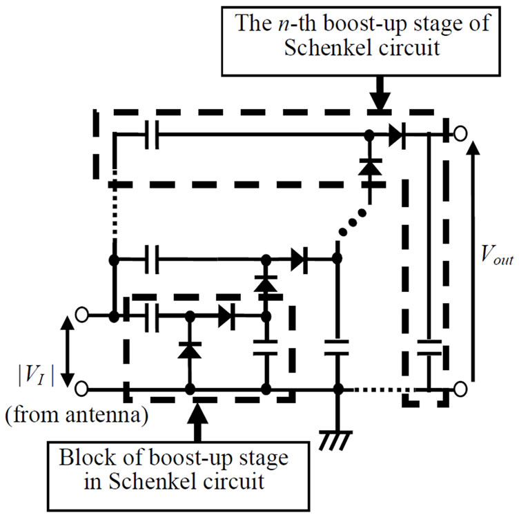
Figure 1. Schematic of Schenkel circuit.
because high-resistivity substrate can be easily introduced [7]. Since the high-resistivity substrate presents not only a low-loss transmission of RF signal [7], but also a low cross-talk in digital circuits [8], various applications are already reported [9,10].
In this paper, we discuss using the SOI-MOSFETbased quasi-diode (SOI-QD) to replace that SBD in Schenkel circuits. First we propose the expression of boost-up efficiency for a low-frequency range using experimental d. c. characteristics of SOI-QD made from various SOI MOSFET’s, and a. c. analyses of SOI-QD are conducted using a two-dimensional (2D) device simulator (ISE DESISS [11]) to investigate operation stability in the RF band. We also define another expression of boost-up efficiency in the RF band, and examined its availability on the basis of a. c. simulation results. RF-band potential of SOI-MOSFET-based quasi-diode is addressed from the viewpoint of future RF applications.
2. Remaining Issues of Conventional Schenkel Circuit and an Advanced Proposal
At first, we used the circuit simulator PSPICE [12,13] to examine the performance of a Schenkel circuit that used Schottky barrier diode (SBD), pn-junction diode (PND) or conventional bulk MOSFET-based quasi-diode (CBQD); in the CB-QD variant, the gate terminal and the drain terminal are connected and the source terminal and the substrate terminal are connected. We assumed that the SBD and PND had a junction area of 46.1 μm2, and that the gate width and the gate length of the bulk MOSFET were 20.6 μm and 0.32 μm. All devices had identical active areas; the junction area of bulk MOSFET is 39.5 μm2. The circuit simulations employed the empirical model (Level = 3) for simplicity [12]. To acquire realistic device performance from the PND and SBD variants, we introduced the minority carrier lifetime model shown in Appendix A.
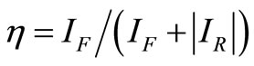
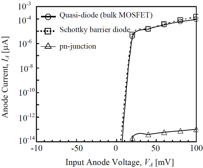
Figure 2 shows simulated rectifier characteristics of the various diodes in a low voltage range of input anode voltage (VA). We can see that SBD with the barrier height (fb) of 0.15 eV has the largest driving current among the three diodes, but it has the highest reverse-biased current (4.43 μA). Figure 3 shows the performance of 5-stage Schenkel circuits that use the three different diodes for an input voltage |VI| of 100 mV. It is shown that the conventional bulk-MOSFET-based quasi-diode (CB-QD) successfully boosts the input signal from a very low level to an acceptable level, while SBD and pn-junction diode fail to do so. SBD failed to match this despite its large driving current; since current SBD designs have a high IR value, almost identical to IF, in the low voltage range of 100 mV, the high leakage current (IR) degrades the signal boost process. On the other hand, the IF and IR values of CB-QD are much smaller than those of SBD. However, CB-QD offers an acceptable level of boost. The main reason is that IF of CB-QD is larger than own IR, which means that the effective boost efficiency (η) of a Schenkel circuit should not be determined by the direct value of driving current, but by the ratio of IF to IR defined as
 . (1)
. (1)
 (a)
(a) (b)
(b)
Figure 2. Forward and reverse characteristics of various diodes (Pspice simulation results). (a) Log scale plot; (b) Linear scale plot.
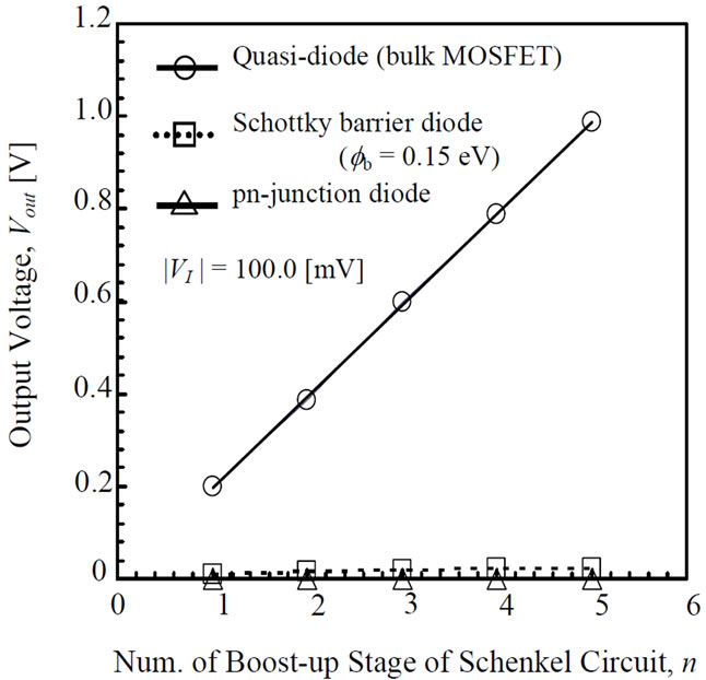
Figure 3. Boost-up performance of Schenkel circuit with various diodes (Pspice simulation results).
In mechanism of voltage boost-up, a large IR value loses a part of charge stored in a capacitor connected in series. So, the above definition of boost-up efficiency is available independently of the number of boost stages on low-frequency conditions where non-local effects are negligibly small. In addition, the voltage across the capacitor rises when the capacitance of the rectifier is larger that of the capacitor connected in series; however, this results in a low-level current source in contrast to the purpose. Therefore, we have to optimize the capacitance of the capacitor so as to fit the performance request.
Unfortunately, we can not apply the above CB-QD to a practical Schenkel circuit as is because it has a crucial drawback; a CB-QD made on an n-channel bulk MOSFET has a parasitic pn-junction diode between the drain and the substrate that can work when the drain is negatively biased. This effective reverse current IR of CB-QD that passes through the parasitic pn-junction diode degrades the η value.
Our solution is to base the quasi-diode on an SOI MOSFET instead of a bulk MOSFET to raise the η value. Figure 4 shows the device structure assumed here and the terminal nodes of an SOI-MOSFET-based quasidiode (SOI-QD). The n-channel fully-depleted (FD)-SOI MOSFET’s used here for evaluation of device performance had channel lengths (L) of 0.32 and 1.0 μm (see Table 1" target="_self"> Table 1); these devices are used only for a feasibility test and they are not well tempered for the present purpose. Later we perform a. c. simulations for SOI-QD. In this case, it is anticipated that the gate-to-source capacitance and the gate-to-drain capacitance play important roles in the a. c. analyses because they yield various parasitic
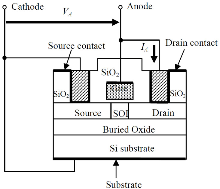
Figure 4. SOI-MOSFET and terminal nodes for quasi-diode operation. Device structure is also assumed for a. c. analyses. Device parameters are carefully designed to take account of practical evaluate gate overlap capacitance, S/D parasitic resistance, fringing capacitance, and other parasitic effects in the device.
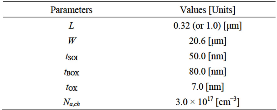
Table 1. Device parameters used in experiments.
capacitances including fringing capacitances [14]. So, we consider a realistic device structure to get reliable a. c. simulation results. All physical parameters to draw the cross-section of device are determined on the basis of 0.4-μm CMOS design rule [15]; they are identical to those of the device used in the present experiments. In simulations described later, the doping level of the SOI layer, Na,ch, was changed from 6.0 × 1016 cm−3 to 3.0 × 1017 cm−3 to adjust the threshold voltage.
Figure 5 shows the ID-VG characteristics of the FDSOI MOSFET’s (L = 0.32 and 1.0 μm) measured at VD = 50 mV; the substrate bias was 0 V. The subthreshold swing (S) values of the two devices are quite different. It can be seen that, because of short channel effects, the S value is larger at L = 0.32 μm than at L = 1.0 μm.
Since it is anticipated that the device characteristics are sensitive to substrate bias (VSUB) because of the thin buried oxide layer, we can produce SOI-QD’s with various rectification characteristics by modifying the substrate bias (VSUB) applied to the FD-SOI MOSFET. It should be noted that this technique is introduced to examine how the threshold voltage of FD-SOI MOSFET modulates the η value through the change of IF and IR. By the substrate bias, we can easily vary the S value and the current level as well as the threshold voltage. As a result, we can find the best solution of the SOI-QD’s rectification characteristics to be tuned. In practical applications, we cannot assume the substrate bias to the device because the assumed RF-ID chip has not a voltage supplier; at the stage of device design, the threshold voltage must be tuned by positive voltage parameter if possible. In this paper, as an attempt, we apply a negative, zero or a positive VSUB value to the device; these conditions are labeled by “A”, “B” or “C” (see Table 2" target="_self"> Table 2), respectively. It should be noted that VSUB value at different L value is not identical when the threshold voltage (VTH) is adjusted to be the same. Figure 6 shows the IA-VA characteristics of SOI-QD “A”, “B” and “C”.
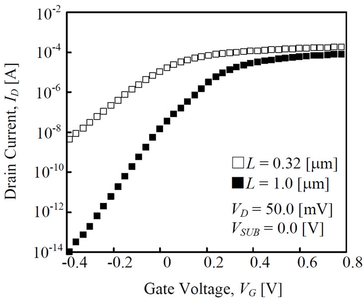
Figure 5. ID-VG characteristics of fully-depleted SOI MOSFET (experimental results).
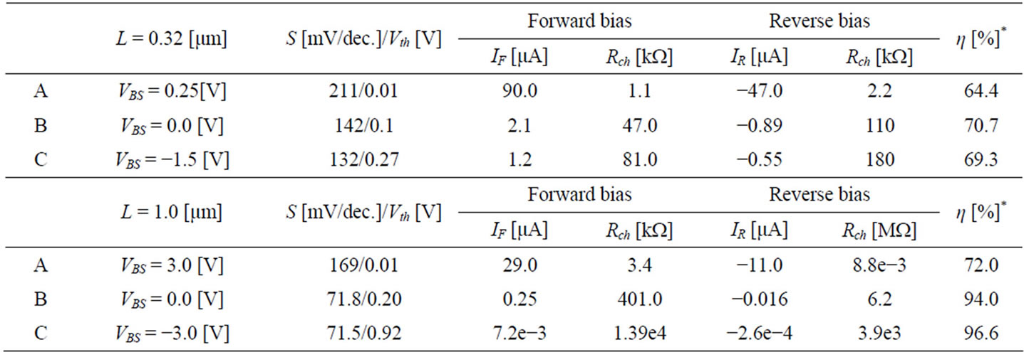
Table 2. IF, IR, Rch, and η values of SOI-QD at various operation conditions (*Amplitude of input signal is 100 mV).
 (a)
(a) (b)
(b)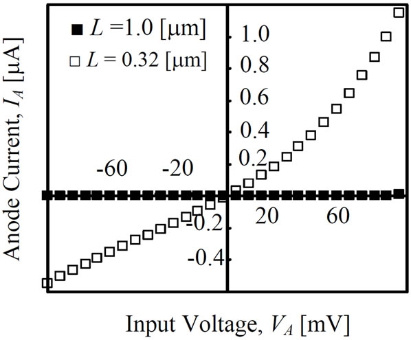 (c)
(c)
Figure 6. Rectifier I-V characteristics of SOI-QD (experimental results). (a) Operation condition “A” (VSUB > 0); (b) Operation condition “B” (VSUB = 0 V); (c) Operation condition “C” (VSUB < 0).
At first, we consider the impact of L value as shown in Figure 6. In condition “A”, the SOI-QD works near the threshold voltage (VTH) because VSUB is positive. S value is large in condition “A” than in condition “B”, resulting in a smaller ratio of IF/IR and thus a smaller η value (see Table 2, and Figures 6(a) and (b)). In condition “A”, however, since the channel resistance (Rch) is reduced due to the lowering of the threshold voltage (VTH), the driving current of the device increases. In contrast, in condition “C”, the device works in the subthreshold region because of the negative substrate bias (VSUB). The S value is smaller in condition “C” than in condition “B”; the channel resistance (Rch) in condition “C” increases due to the raising of the threshold voltage (VTH), resulting in a lower drive current, but identical η value to that seen in condition “B” (see Figure 6(c)).
Next we compare the performance of the two devices (L = 1.0 and 0.32 μm) shown in Figure 6. As mentioned above, the S value with L = 1.0 μm is smaller than that with L = 0.32 μm. Accordingly, IF/IR is larger with L = 1.0 μm than that with L = 0.32 μm, and the η value with L = 1.0 μm is larger than that with L = 0.32 μm as shown in Table 2. It should be noted that the difference in forward current level (IF) at the same bias comes from not only the different W/L value but also the different S value. This means that we must take account of the trade-off between η and IF; that is, it is necessary to select the most suitable operation bias condition and to reduce the S value. Table 2 suggests that the S value should be less than 75 mV/dec to reduce IR value and threshold voltage should be ranging from 0.1 V to 0.2 V to simultaneously gain a high η value.
Finally, we briefly compare the performance of SBD, pn-junction diode and SOI-QD; Table 2 shows IF, IR and η of SOI-QD at various operation conditions when the input signal amplitude (|VA|) is 100 mV. According to a recent report [3], when VA = 100 mV, the SBD has an IF value of about 1.0 nA and the pn-junction diode has an IF value of about 0.1 pA; this indicates that the SOI-QD has identical IF to the other devices or has larger IF at all conditions for the two L values examined. In addition, since the SOI MOSFET has lower leakage current than the SBD and subthreshold characteristic of well-tempered SOI MOSFET is excellent, a high boost efficiency can be expected when the SOI-QD is used.
3. Simulation-Based Consideration of RF Performance of SOI-QD
In order to investigate of the feasibility of using SOIQD’s in RF applications [16], we conducted extensive a. c. analyses using a 2D device simulator [11]. Figure 7" target="_self"> Figure 7 shows the simulated rectifier characteristics of the SOIQD for various Na,ch values. Since the threshold voltage (Vth) rises sharply with the increase in doping level of the SOI layer (Na,ch), the forward-biased anode current (IF) decreases greatly and the reverse-biased anode current (IR) also decreases. However, η increases on the basis of Equation (1) as Na,ch increases because the reduction of IR overwhelms that of IF, which is as is expected. A simple estimation method of η value of SOI MOSFET is shown in Appendix B.
When a high-frequency operation is considered, a. c. response to applied signal amplitude should be evaluated; this is very important in SOI MOSFET because it is anticipated that the floating-body effect delays the current response to the applied signal [17]. We think that anode conductance gA (=dIA/dVA) successfully traces response capability of SOI MOSFET because gA is extracted from a small signal analysis; we think a large signal analysis is not always required because Fourier transformation results of signals are effectively considered. Then we define the boost-up efficiency to a. c. signals as
 , (2)
, (2)
where gAF and gAR mean the anode conductance at the forward and the backward bias conditions, respectively;

Figure 7. Simulated I-V characteristics of quasi-diodes (device simulations).
IAF and IAR are the anode current at the forward and the backward bias conditions, respectively. Some Figure 8 shows the simulated gA-VA curves for various Na,ch values, where gA (=dIA/dVA). Figure 8(a) is for Na,ch = 5 × 1016 cm−3, Figure 8(b) for Na,ch = 1 × 1017 cm−3, and Figure 8(c) for Na,ch = 3 × 1017 cm−3. Frequency f was changed from 1 Hz to 10 GHz. In the case of Na,ch = 5.0 × 1016 cm−3 (see Figure 8(a)), the gA-VA characteristic is not sensitive to frequency (1 Hz to 10 GHz). In the cases of Na,ch = 1.0 × 1017 cm−3 (see Figure 8(b)) and 3.0 × 1017 cm−3 (see Figure 8(c)), however, the gA-VA characteristic is sensitive to frequency. In particular, for Na,ch = 3.0 × 1017 cm−3, the gA-VA characteristic reacts strongly to frequency.
 (a)
(a) (b)
(b) (c)
(c)
Figure 8. Simulated gA-VA characteristics (device simulations). (a) Na,ch = 5.0 × 10¹⁶ [cm−3]; (b) Na,ch = 1.0 × 10¹⁷ [cm−3]; (c) Na,ch= 3.0 × 10¹⁷ [cm−3].
Since the SOI layer is 50 nm thick, the fully-depleted condition is satisfied in two cases (Figures 8(a) and (b)) [18]. Majority carriers (holes) are basically not responsible for device operation, and so the parasitic bipolar action is not expected at the bias condition used (|VA| < 0.3 V). Since the threshold voltage is very low (~0 V), electrons in the inversion layer rule device operation; in this case, the frequency dependence of the dielectric response of electrons (“majority carriers” near the surface) limits the gA-VA characteristic. The limit of the frequency response of electrons in Si is higher than 100 GHz [16], so the simulation results shown in Figures 8(a) and (b) are acceptable. The smaller variation in gA-VA characteristics seen in Figure 8(b) is related to the remaining hole density near the bottom of SOI layer, which should be higher than that in Figure 8(a).
We note that the fully-depleted condition is not satisfied in the case of Na,ch = 3.0 × 1017 cm−3 [18]. That is, the majority carriers (holes), remaining near the SOI/ buried oxide interface, play an important role in determining device operation, which corresponds to the typical floating body effect [17]. Since the gA-VA characteristics at frequencies above 10 MHz differ from those below 10 MHz as seen in Figure 8(c); in other words, the gA-VA characteristics at frequencies above 10 MHz are not normal. In the present case, it is easily anticipated that the generation process of majority carriers (holes) (around the junction and inside the depleted body) rules the dynamic operation of SOI-QD. Since the generationrecombination time constant is about 0.1 μsec in the present simulations (see Appendix A), the hole generation process does not respond at frequencies above 10 MHz, resulting in the body floating effect [17].
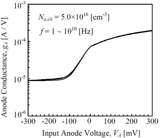
Figure 9 shows the simulated η − f characteristics of the SOI-QD from f = 1 Hz to 1 THz with the parameter of Na,ch, although the simulated value of η is not reliable for f > 100 GHz because physical models for devices in the device simulator [11] are not proposed for such a high frequency; we simply focus on the behavior of η. η values shown in Figure 9 are calculated by Equation (2).

Figure 9. η-f characteristics for various body doping levels (device simulations).
In Figure 9, it should be noted that η values calculated by gA (Equation (2)) at low frequency region are almost identical to η values calculated from d. c. current (experimental results) for L = 1.0 μm by Equation (1). So this suggests that η value can be estimated using Equation (2) at RF region. In Figure 9, we can see that the η value remains higher than 90% independently of Na,ch up to 10 MHz; this is supported by the fact that S value in the active range of IA of SOI-QD is sufficiently small. However, when f is higher than 100 MHz, especially when Na,ch = 3.0 × 1017 cm−3, η falls to 60%. This comes from the body-floating effect as mentioned previously. On the other hand, at Na,ch = 5.0 × 1016 cm−3 and 1.0 × 1017 cm−3, η remains high up to 10 GHz. As a result, SOI-QD’s with Na,ch = 5.0 × 1016 cm−3 and 1.0 × 1017 cm−3 can be used in RF applications; when Na,ch = 3.0 × 1017 cm−3, the SOI-QD is no longer suitable because of the significant body floating effect.
Figure 10 shows the simulated η-Na,ch characteristics of the SOI-QD at 1 MHz and 4 GHz. In the low frequency range (~1 MHz) η slightly increases with Na,ch because of the reduction of S at the driving point, and finally reaches its upper limit when the reduction in S value ceases. Since Na,ch increases, driving current (IA) decreases because the threshold voltage of FD-SOI MOSFET rises. Thus, the doping level of the SOI layer of SOI-QD must be optimized to realize a high performance Schenkel circuit. In the radio frequency range (~4 GHz), η peaks because of the floating body effect mentioned above. This strongly suggests that the value of Na,ch must be selected so as to hold the SOI layer in the fully-depleted condition of the SOI layer. As for the present simulation, Na,ch = 1.0 × 1017 cm−3 yields the best SOI-QD performance in RF applications up to 100 GHz; when SOI layer is thinned to a range of sub-50 nm, Na,ch value higher than 1 × 1017 cm−3 can be applied to devices [19].
In the above simulations, we assumed VA = 0.1 V because we considered the case of short-distance communications. Since the above simulations show that the pro-
Figure 10. η-Na,ch characteristics for various frequencies (device simulations).
posed SOI-QD produces almost identical performance at VA < 0.1 V, we think that Schenkel circuits with SOI-QD’s are also applicable to long-distance communications.
4. Conclusion
The feasibility replacing SBD’s in the Schenkel circuit with SOI-MOSFET’s as quasi-diodes was examined by experiments and simulations. The reverse-biased current (IR) of the SOI-QD is much lower than its forward-biased current (IF) and the driving current (IF) is high because of the excellent S value provided by the SOI-MOSFET arrangement; we noted that the trade-off between boost efficiency (η) and IF should be taken into account. In addition, a. c. analyses using a two-dimensional device simulator showed that the body doping concentration (Na,ch) of the SOI layer should be optimized so as to hold the fully-depleted condition for RF applications up to 100 GHz.
5. Acknowledgements
This study is financially supported by Kansai University research grants, Grant-in-Aid for Joint Research (2004-2005). The authors wish to express their thanks to Mr. Takuta Tamura, Mr. Yuki Tahara, and Mr. S. Namura for their technical support on device simulations.
REFERENCES
- U. Karthaus and M. Fischer, “Fully Integrated Passive UHF RFID Transponder IC with 16.7-μW Minimum RF Input Power,” IEEE Journal of Solid-State Circuits, Vol. 38, No. 10, 2003, pp.1602-1608.
- M. Usami and M. Ohki, “The μ-Chip: Ultra-Small 2.45 GHz RFID Chip for Ubiquitous Recognition Applications,” IEICE Transactions on Electronics, Vol. E86-C, No. 4, 2003, pp.521-528.
- W. Jeon, T. M. Firestone, J. C. Rodgers and J. Melngailis, “Design and Fabrication of Schottky Diode, On-Chip RF Power Detector,” Solid-State Electronics, Vol. 48, No. 10-11, 2004, pp. 2089-2093.
- B. Strassner and K. Chang, “Passive 5.8-GHz Radio-Frequency Identification Tag for Monitoring Oil Drill Pipe,” IEEE Transactions on Microwave Theory and Techniques, Vol. 51, No. 2, 2003, pp. 356-363. doi:10.1109/TMTT.2002.807832
- K. Ahsan, H. Shah and P. Kingston, “RFID Applications: An Introductory and Exploratory Study,” International Journal of Computer Science Issues, Vol. 7, No. 1, 2010, pp. 1-7.
- Y. Kado, M. Suzuki, K. Koike, Y. Omura and K. Izumi, “A 1 GHz/0.9 mW CMOS/SIMOX Divide-by-128/129 Dual-Modulus Prescaler Using a Divide-by-2/3 Synchronous Counter,” IEEE Journal of Solid-State Circuits, Vol. 28, No. 4, 1993, pp. 513-517.
- O. Rozeau, J. Jomaah, J. Boussey and Y. Omura, “Comparison between Highand Low-Dose Separation by Implanted Oxygen MOS Transistors for Low-Power RadioFrequency Applications,” Japanese Journal of Applied Physics, Vol. 39, No. 4B, 2000, pp. 2264-2267. doi:10.1143/JJAP.39.2264
- J. P. Raskin, A. Viviani, D. Flandre and J.-P. Colinge, “Substrate Crosstalk Reduction Using SOI Technology,” IEEE Transactions on Electron Devices, Vol. 44, No. 12, 1997, pp. 2252-2261. doi:10.1109/16.644646
- Y. Omura, “Negative Conductance Properties in Extremely Thin Silicon-on-Insulator Insulated-Gate pn-Junction Devices (Silicon-on-Insulator Surface Tunnel Transistor),” Japanese Journal of Applied Physics, Vol. 35, No. 11A, 1996, pp. L1401-L1403. doi:10.1143/JJAP.35.L1401
- Y. Omura and T. Tochio, “Significant Aspects of Minority Carrier Injection in Dynamic-Threshold SOI MOSFET at Low Temperature,” Cryogenics, Vol. 49, No. 11, 2009, pp. 611-614. doi:10.1016/j.cryogenics.2008.11.009
- Synopsys Inc., “TCAD-DESSIS/GENESISe Operation Manual,” ver. 7.5. http://www.sysnopsys.com/
- Microsim Corp., “PSpice Reference Manual.” http://www.microsimcom.com/
- K. Takahashi, S. Y. Wang and M. Mizunuma, “Complementary Charge Pump Booster,” Electronics and Communications in Japan Part II-Electronics, Vol. 82, No. 6, 1999, pp. 73-81. doi:10.1002/(SICI)1520-6432(199906)82:6<73::AID-ECJB8>3.0.CO;2-C
- Y. Taur and T. H. Ning, “Fundamentals of Modern VLSI Devices,” Cambridge University Press, Cambridge, 1998.
- Y. Kado, M. Suzuki, K. Koike, Y. Omura and K. Izumi, “An Experimental Full-CMOS Multi-gigahertz PLL LSI Using 0.4-μm Gate Ultrathin-Film SIMOX Technology,” IEICE Transactions on Electronics, Vol. E76-C, No. 4, 1993, pp. 562-571.
- C. Wann, F. Assaderaghi, L. Shi, K. Chan, S. Cohen, H. Hovel, K. Jenkins, Y. Lee, D. Sadana, R. Viswanathan, S. Wind and Y. Taur, “High-Performance 0.07-μm CMOS with 9.3-ps Gate Delay and 150 GHz fT,” IEEE Electron Devices Letters, Vol. 18, No. 12, 1997, pp. 625-627. doi:10.1109/55.644091
- J.-P. Colinge, “Silicon-on-Insulator: Materials to VLSI,” 3rd Edition, Kluwer Academic Publishing, Dordrecht, 2004. doi:10.1007/978-1-4419-9106-5
- Y. Omura, S. Nakashima and K. Izumi, “Investigation on High-Speed Performance of 0.1-μm-Gate, Ultrathin-Film CMOS/SIMOX,” IEICE Transactions on Electronics, Vol. E75-C, No. 12, 1992, pp. 1491-1497.
- Y. Omura, S. Nakashima, K. Izumi and T. Ishii, “0.1-μmGate, Ultrathin-Film CMOS Devices Using SIMOX Substrate with 80-nm-Thick Buried Oxide Layer,” IEEE Transactions on Electron Devices, Vol. 40, No. 5, 1993, pp. 1019-1022. doi:10.1109/16.210214
- J. R. Brews, “A Charge-Sheet Model for the MOSFET,” Solid State Electronics, Vol. 21, No. 2, 1978, pp. 345-355. doi:10.1016/0038-1101(78)90264-2
- Y. Sakurai, A. Matsuzawa and T. Dozeki, Eds., “FullyDepleted SOI CMOS Circuits and Technology for Ultralow-Power Applications,” Springer, Berlin, 2006.
Appendix A: Simulation Model for Minority Carrier Lifetime
Here we introduce the model for minority carrier lifetimes [11] used in PSPICE simulations to ensure consistency with DESSIS simulation results.
 , (A1)
where N is the doping density, Nref is the doping parameter, γ is the fitting parameter, τmax and τmin are lifetime parameters. Parameter values used here are summarized in Table 3.
Appendix B: On the Design Guideline of SOI-QD’s
We rewrite the expression of boost-up efficiency given by Equation (1).
 , (B1)
When no short-channel effect is assumed, IF and IR can be expressed approximately as
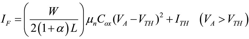 ,(B2)
,(B2)
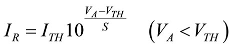 , (B3)
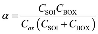
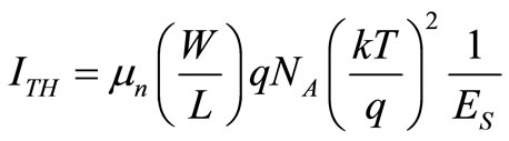
where most of notations are conventional, and S stands for the subthreshold swing for the fully-depleted SOI MOSFET [17]. Parameters α and ITH (threshold current) are given by
 , (B4)
 , (B5)
where CSOI is the SOI layer capacitance [17], CBOX is the buried oxide layer capacitance [17], and Es is the surface electric field. The derivation of α is given in [17], and that of ITH is given in [20,21].
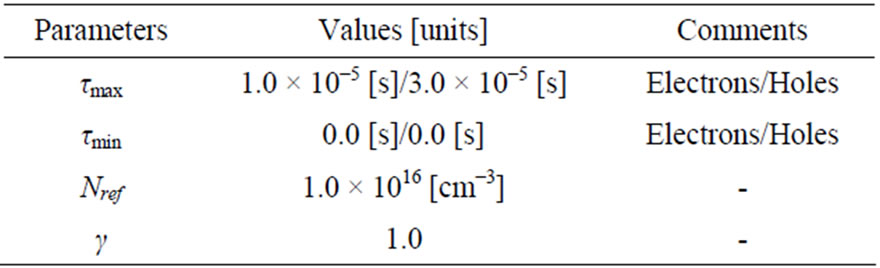
Table 3. Physical parameters assumed in device simulations (DESSIS).