Circuits and Systems
Vol. 3 No. 1 (2012) , Article ID: 16607 , 6 pages DOI:10.4236/cs.2012.31007
The Effects of Fabrication Prameters and Electroforming Phenomenon on CdTe/Si (p) Heterojunction Photovoltaic Solar Cell
Communications & Electronics Department, Faculty of Engineering, Philadelphia University, Amman, Jordan
Email: wagahfaljubori@yahoo.com
Received September 8, 2011; revised October 8, 2011; accepted October 16, 2011
Keywords: CdTe Solar Cells; CdTe/Si Heterojunction; In-Doped CdTe
ABSTRACT
The In-doped CdTe/Si (p) heterostruture was fabricated and its electrical and photoelectrical properties were studied and interpreted. During the fabrication processes of CdTe/Si heterojunction, some practical troubles were encountered. However, the important one was the formation of the SiO2 thin oxide layer on the soft surface of the Si during the formation of the back contact. The silicon wafer was subjected to different chemical treatments in order to remove the thin oxide layer from the silicon wafer surfaces. It was found that the heterojunction with Si (p+) substrate gave relatively high open circuit voltage comparing with that of Si (p) substrate. Also an electroforming phenomenon had been observed in this structure for the first time which may be considered as a memory effect. It was observed that there are two states of conduction, non-conducting state and conducting state. The normal case is the non-conducting state. As the forward applied voltage increased beyond threshold value, it switches into the conducting state and remains in this state even after the voltage drops to zero.
1. Introduction
In recent years much attention had been paid to the heterojunction devices research [1]. The success of heterojunctions is fully established in electronic devices including solar cells high quality lasers, and optical detectors [2]. Heterojunctions which consist of CdTe as one of the junction sides had been under investigation for many years. Mohamed et al. [3] also studied the electrical properties of post-deposition annealed and asdeposited In-doped CdTe thin films, it was observed that the CdTe film was of modified Poole-Frenkel conduction mechanism and the resistivity of the film could be lowered by more than one order of magnitude due to indium doping. Also, considerable amount of work had been paid to develop the CdS/CdTe solar cells over the last ten years [4,5]. Levi [6] also studied the electrical, photo-electrical, and structural properties of CdS/CdTe heterostruture. High efficiency solar cells of efficiencies up to 12.5% were developed with a CdTe low temperature (>450˚C) process [7]. Efficient solar cell performance requires minimizing the forward recombination current and maximizing the light generated current. Collection losses can be minimized in thin film of high absorption and short diffusion length. Voltage dependent photocurrent collection losses in CdTe films were observed [8]. The voltage dependence of photo current of CdTe/CdS solar cells was characterized by separating the forward current from the photocurrent.
2. CdTe/Si Heterojunctions Properties
Mohamed et al. [9] have studied the photovoltaic properties of In-doped CdTe (p) homojunction structure. It was revealed that the In-doped CdTe thin film is of high bulk resistivity, which affects its photovoltaic properties. The deteriorative effect of high bulk resistivity increases by increasing the light intensity which in turn limits the benefit of using higher light intensity that improves the conversion efficiency. A new factor denoted as “S” was devised to measure how the series resistance affects the short circuit current versus light intensity characteristics of the new structure and generalized conclusions were put forward to cover all types of the conventional solar cells. The In-doped CdTe (p) thin film is of high bulk resistivity which largely affects its photovoltaic properties particularly the short circuit current. It was noted that, the deteriorative effect of the high bulk resistivity increases by increasing the light intensity, which in turn limits the benefit of using light concentrators that improve the short circuit current. Birnkmanm and Alamri [10] found that the use of post deposition heat treatment would probably reduce the bulk resistance and possibly improves contact performance. It was proved previously [4] that the polarity of the applied voltage had almost no effect on the I-V characteristics of Al-In doped-CdTe-Al structure annealed at 100˚C, which means that the contacts are ohmic. Variation of bulk resistivity with the diffusion temperature is shown in Figure 1. It can be observed that the bulk conductivity of the doped (diffused) films is about one order higher than that of the undoped CdTe films. This is due to the incorporation of Indium atoms that acts as donor sites, which in turn increases the carrier concentration. This will decrease the barrier height at the grain boundaries, resulting in less impedance to the carrier transport [11]. Also it was found that the maximum bulk conductivity is occurred at 100˚C diffusion temperature.
There is intensive interest to develop high efficiency multi-junction solar cells including the exploration of using silicon (Si) substrate. Heterojunction devices have been realized by depositing phosphorus-doped silicon (Si) (n-type) on a p-type crystalline silicon substrate. The open circuit voltage increases proportionally to the band gap, whereas the number of absorbed photons, i.e., the current decreases with broadening the band gap. The resulting power, as the product of voltage and current, has a maximum value at 1.3 eV. Silicon with the band gap of 1.1 eV and CdTe with 1.5 eV are close to this optimal value. Consistent growth of laterally uniform CdTe (CT) on Si substrate by molecular beam epitaxy has been reported, which indicates that II-VI semiconductor alloys based on CdTe and grown on Si substrates may give good cell performance [12]. Recent nanostructures materials (nanocrystal incorporated in isolators) are used for windows. Electrons can migrate in these structures from one nanocrystal (nc) to adjacent nc and to electrode by tunnel effect, therefore such materials are conductive. Usually nc of the same material as in solar is used for window. Thus, CdTe nc can be used for CdTe solar cell window. Then n-type Si nc on p-type bases is a possible perspective [13].
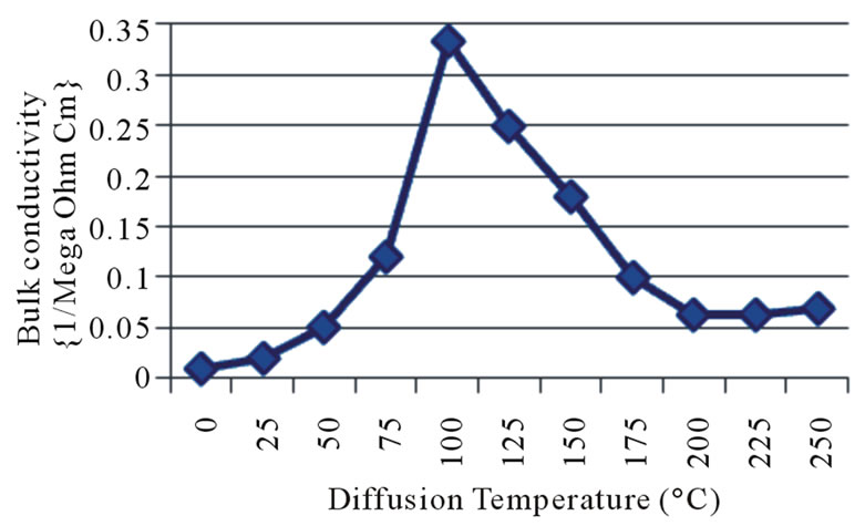
Figure 1. Bulk conductivity vs. diffusion temperatures of In-doped CdTe thin films.
3. Laboratory Preparation
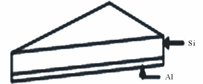
The samples that will be discussed in this paper are of common evaporation conditions. Few samples of CdTe thin films were prepared by thermal evaporation and deposited on Si substrate. The deposition parameters and the sequence of fabricating In-doped CdTe/Si (p) structure are as follow (see Figure 2):
 (a)
(a)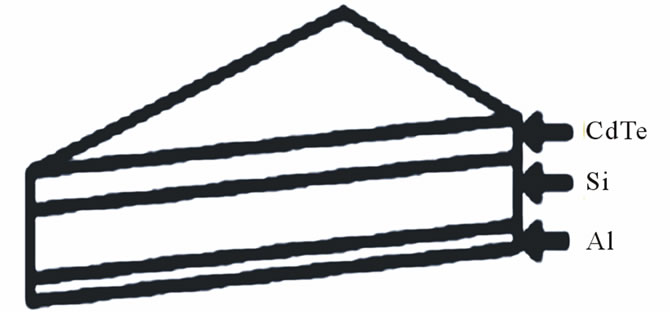 (b)
(b)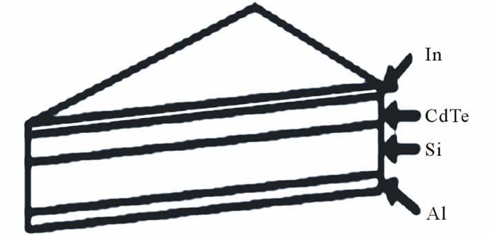 (c)
(c)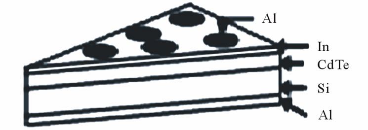 (d)
(d)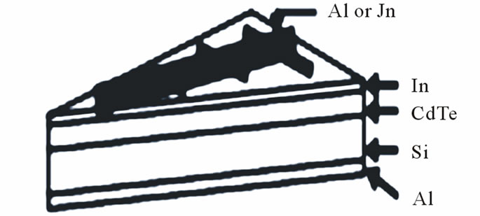 (e)
(e)
Figure 2. The sequence of preparing In (Al)-In-doped CdTe/Si-Al structure.
(a) Deposition of Al back contact 2000 Å on the back surface of the silicon wafer.
(b) Deposition of CdTe layer of 4000 Å thickness (since the photosensitivity of the evaporated CdTe shows a relatively high value at this thickness [14]) with 8 Å/s rate of deposition and at 25˚C substrate temperature. The next step is annealing process at 200˚C (under vacuum) for an hour in order to anneal the CdTe layer and to support back contact formation.
(c) Deposition of indium layer with 100 Å thickness, on top of the CdTe layer followed by Indium diffusion in CdTe by heating process at 100˚C under vacuum for an hour.
(d) and (e) deposition of aluminum or indium top contact.
In this paper different structures will be studied. So, for the sake of simplicity, some symbols will be used so that one can easily recognize the different structures. These symbols will be used as superscript incorporated on the letters that describe different structure layers. For instance, the structure In*-In~* CdTe/Si (p) indicates and from right to left that: a silicon wafer (p-type) on which a CdTe layer is deposited, In~* denotes an indium layer diffused in the CdTe layer in dot-shaped form, so the superscript (~) represents a diffused layer followed by the superscript (*) denotes the shape of the diffused layer in dotshaped form. In* denotes indium top contact in dot-shaped form. In this paper the following superscripts will be used: (*): denotes a dot shape, (~): denotes a diffused layer and (#): denotes a grid shape, usually used for top contacts.
During the fabrication processes of CdTe/Si heterojunction, some practical troubles were encountered. However, the important one is the formation of the SiO2 thin oxide layer on the soft surface of the Si during the formation of the back contact. The silicon wafer is subjected to different chemical treatments in order to remove the thin oxide layer from the silicon wafer surfaces. Then the sequence of fabrication the on Al-CdTe/Si (p)-Al structure is as follow:
1) Deposition of Al back contact.
2) Formation of the back contact by annealing process at 200˚C for an hour (under vacuum).
3) Deposition of CdTe layer.
4) Deposition of Al top contact.
During the formation of the back contact, a thin oxide layer (SiO2) is grown undeliberately. The existence of this layer is investigated practically by fabrication of Al-Si-Al structure with back contact formation as in steps 1 and 2 above, after which a top contact Al is deposited. Figure 3 illustrates the (I-V) characteristics of the device, which exhibits a diode effect that consequently indicates the formation of a MOS diode (AlSiO2-Si-Al). The existence of the oxide layer badly affects the (I-V) characteristics of the structure AlCdTe/Si (p)-Al.
Figure 4 depicts the (I-V) characteristics of the CdTe/Si with the interfacial oxide layer with different CdTe thicknesses. It can be deduced that the characteristics are not of a PN junction (no rectification effect) due to the interfacial oxide layer which prevents the establishment of heterojunction between CdTe and Si. Evidently the introduction of oxide layer increases the total absorption depth. This in turn utilizes the wasted portion of the solar spectrum, consequently increases the short circuit current [15,16].
4. The Effect of Top Contact Material
Two metals are used as top contacts they are, indium and aluminum. Figure 5 illustrates the dark (I-V) characteristics of the structure In~-CdTe/Si (p) with two top contact materials: indium and aluminum in dot-shaped form. The two devices are fabricated under the same evaporation conditions and for the same time. It is observed that the device with indium top contact has a good rectification characteristic comparing with that of the aluminum top contact. Since the bending of the forward dark (I-V) characteristic towards the voltage axis is indicative of high series resistance [17], the conclusion that aluminum metal shows a high ohmic contact resistance to the In~-CdTe (In-doped CdTe) is valid. The two devices had
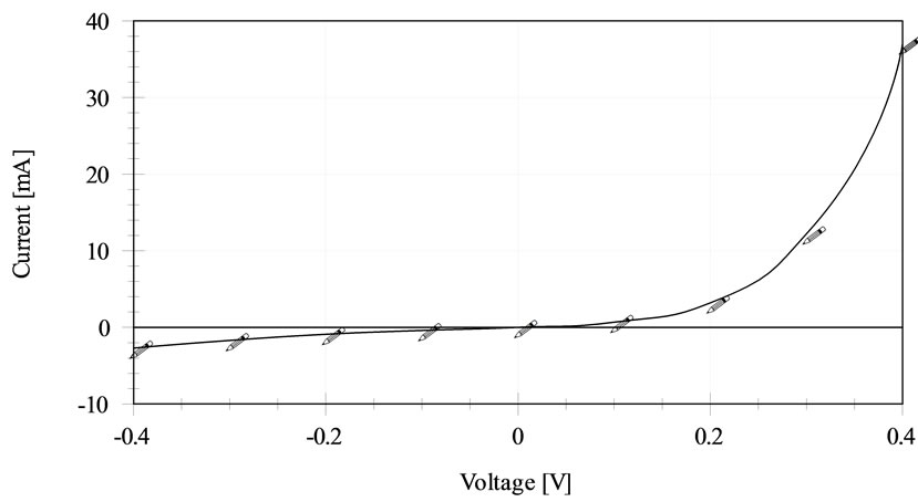
Figure 3. I-V characteristics of Al-Si (p)-Al.
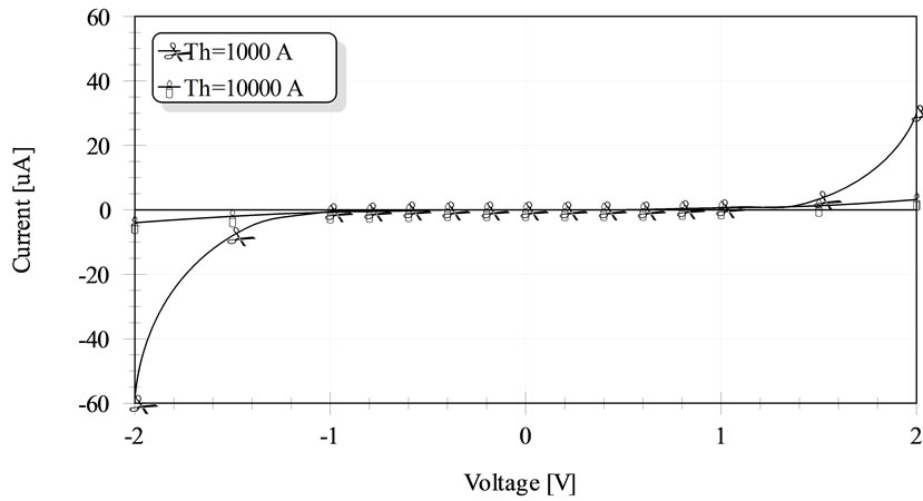
Figure 4. I-V characteristics of CdTe/Si (p) with interfacial oxide layer for different CdTe thicknesses.
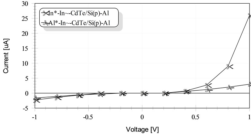
Figure 5. I-V characteristics of In-doped CdTe/Si (p) for In and Al top contacts in dot-shaped form.
equal open circuit voltage of about 20 mV at 75 mW/cm2 light intensity with very low short circuit current.
Figure 6 depicts the dark (I-V) characteristics of the same structure but with indium and aluminum top contacts in grid form. It is noted that the device with indium top contact has also a good rectification characteristic supporting the conclusion that indium metal shows better ohmic contact comparing to aluminum metal.
5. The Effect of Device Area
Figure 7 illustrates a comparison between the dark (I-V) characteristics of device areas 1 cm2 and 3 mm2. Indium was used as a top contact in grid form in the large area device, and in dot-shaped form in the small area one. It is clear that the increase in the top contact area increases the current flowing in the device due to the relatively low bulk resistance. It was found that the large area device showed an open circuit voltage greater than that of the small area, 36 mV and 20 mV respectively at 75 mW/cm2 light intensity. The slight increase in the open circuit voltage due to area increase of the device may be attributed to the increase in the photo generated current by increasing the device area, this in turn increases the open circuit voltage.
6. The Effect of Silicon Concentration
The dark (I-V) characteristics of the two structures In~-CdTe/Si (p+) and In~-CdTe/Si (p) are discussed. Figure 8 shows that the leakage current in the former structure is more than in the latter. This effect can be explained in terms of silicon concentration as follows: in the case of Si (p+), the depletion region is narrow due to the high holes concentration in the silicon, while in the case of Si (p) the low holes concentration results in a wider depletion region and consequently the low leakage current. The device with Si (p+) showed an open circuit voltage of 100 mV at 75 mW/cm2 light intensity due to the increase in the holes concentration in the silicon, this, in turn increased the junction abruptness that increase the open circuit voltage.
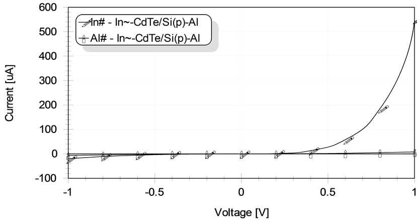
Figure 6. I-V characteristics of In-doped CdTe/Si (p) for In and Al top contacts in grid form.
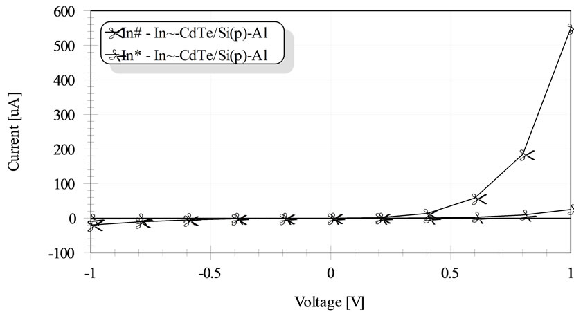
Figure 7. I-V characteristics of In-doped CdTe/Si (p) for In top contacts in dot-shaped and grid forms.
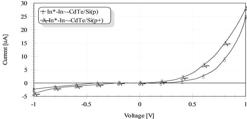
Figure 8. I-V characteristics of In-doped CdTe/Si (p) and In-doped CdTe/Si (p+) structures.
7. Electro Forming Phenomenon
It was found that in high electric field the (I-V) characteristics exhibited unusual behaviors as shown in Figure 9. It was observed that there were two states of conduction, non-conducting state represented by the curve AB and conducting state represented by the curve CD. The normal case is the non-conducting state. As the forward applied voltage was increased beyond the threshold value (7 V), it switched to the conducting state and remained in this state even after the voltage dropped to zero.
This behavior is similar to the electroforming phenomenon observed in metal-insulator-metal structure that is explained in terms of filamentary conduction model [18]. In this model, the conduction takes place through
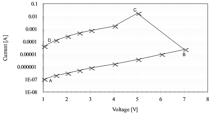
Figure 9. Forming effect in CdTe/Si (p) with interfacial oxide layer with CdTe thickness of 5740 Å.
highly conductive filaments that are created during the Forming process, that bridge the insulating layer between the electrodes. Here the insulating layer consists of two sub-layers, the oxide layer and the semi-insulating CdTe layer. It is observed that when the samples remain under conducting state for several minutes, during which high current flows through the sample, the samples drops to its non-conducting state suddenly. This may be attributed to the rupturing of the conductive filaments due to the relatively high local temperature arises from high current flow. This phenomenon is observed for several samples prepared with different CdTe thicknesses.
8. Conclusions
The heterojunction structure In-doped CdTe/Si (p) has poor photovoltaic properties due to the high resistivity of CdTe film and due to the large mismatch between CdTe and Si. It is observed that the Indium metal makes a good ohmic contact to the In-doped CdTe thin film comparing with the Aluminum metal. The heterojunction In-doped CdTe/Si (p+) has shown a relatively high open circuit voltage comparing with that of the Si (p) substrate due to higher junction abruptness that improve the photovoltaic action in the structure. Finally, an electroforming phenomenon has been observed in the CdTe/Si (p) heterojunction which may be considered as a memory effect.
REFERENCES
- L. M. Woods, D. H. Levi, V. Kaydonov, G. Y. Robinson and R. K. Ahrenkiel, “Electrical Characterization of CdTe Grain Boundary Properties from as-Processed CdTe/CdS Solar Cells,” 2nd World Conference and Exhibition on Photovoltaic Solar Energy Conversion, Vienna, 6-10 July 1998, pp. 1043-1049.
- P. Fernández, J. Solisa and J. Piqueras, “Pulsed Laser Annealing of CdTe Single Crystals,” Journal of Optoelectronics and Advanced Materials, Vol. 2, No. 3, 2000, pp. 235-240.
- W. F. Mohamed and M. A. Shehathah, “The Electrical Properties of Post-Deposition Annealed and As-Deposited In-doped CdTe Thin Films,” Renewable Energy Journal, Vol. 26, 2002, pp. 285-294. doi:10.1016/S0960-1481(00)00195-6
- X. Mathew, J. P. Enriquez, A. Romeo and A. N. Tiwari, “CdTe/CdS Solar Cells on Flexible Substrates,” Solar Energy Journal, Vol. 77, 2004, pp. 831-838. doi:10.1016/j.solener.2004.06.020
- T. Potlog, “Development of New Techniques of CdS/ CdTe Solar Cell Enhancement,” International Semiconductor Conference, Sinaia, 27-29 September 2006, pp. 171-174. doi:10.1109/SMICND.2006.283960
- D. H. Levi, L. M. Woods, D. S. Albin and T. A. Gessert,, “The Influence of Grain Boundary Diffusion on the Electro-Optical Properties of CdTe/CdS Solar Cells, Austria,” 6-2nd World Conference and Exhibition on Photovoltaic Solar Energy Conversion, Vienna, 10 July 1998. pp. 1057-1062.
- G. Khrypunov, A. Romeo, F. Kurdesau, D. Batnzer, H. Zogg and D. L. Tiwari, “Recent Development in Evaporated CdTe Solar Cells,” Solar Energy Material and Solar Cells, Vol. 90, 2006, pp. 664-677. doi:10.1016/j.solmat.2005.04.003
- S. Hegedus, D. Desai and C. Thompson, “Voltage Dependent Photocurrent Collection in CdTe/CdS Solar Cells,” Progress in Photovoltaics: Research and Applications, Vol. 15, No. 7, 2007, pp. 587-602. doi:10.1002/pip.767
- W. F. Mohamed and M. A. Shehathah, “The Effect of the Series Resistance on the Photovoltaic Properties of In-Doped CdTe (p) Thin Film Homojunction Structure,” Renewable Energy Journal, Vol. 21, No. 2, 2000, pp. 141-152. doi:10.1016/S0960-1481(00)00008-2
- A. W. Brinkman and S. M. Al-Amri, “Thin Film CdTe Based Solar Cell,” Proceedings of the Sixth Arab International Solar Energy Conference, Muscat, Sultanate of Oman, 29 March 1998, p. 752.
- W. Huber and A. Lopez, “The Electrical Properties of CdTe Films Grown by Hot Wall Epitaxy,” Thin Solid Films, Vol. 58, 1979, pp. 21-27. doi:10.1016/0040-6090(79)90201-3
- Y. G. Xiao, Z. Q. Li, M. Lestrade and Z. M. Simon Li, “Modeling of CdZnTe/CdTe/Si Triple Junction Solar Cells,” 37th IEEE Photovoltaic Specialists Conference PVSC, No. 604, 2011, pp. 14-16.
- S. Park, E. Cho, D. Song, G. Conibeer and M. Green, “n-Type Silicon Quantum Dots and p-Type Crystalline Silicon Heteroface Surface Solar Cells,” Solar Energy Materials & Solar Cells, Vol. 93, No. 6-7, 2009, pp. 684- 690. doi:10.1016/j.solmat.2008.09.032
- S. Saha, U. Pal, B. K. Samantaray, A. K. Chaudhuri and H. D. Banerjee, “Structural Characterization of Thin films Cadmium Telluride,” Thin Solid Films, Vol. 164, 1988. pp. 85-89. doi:10.1016/0040-6090(88)90114-9
- W. F. Mohamad and A. M. Mustafa, “The Influence of Defects on Short Circuit Current Density in p-I-n Silicon Solar Cell,” Renewable Energy Journal, Vol. 30 No. 2, 2005, pp. 187-193. doi:10.1016/j.renene.2004.03.012
- W. F. Mohamad, A. Abuhajar and A. N. Saleh, “Effect of Oxide Layers and Metals on Photoelectric and Optical Properties of Schottky Barrier Photo Detector,” Renewable Energy Journal, Vol. 31, No. 10, 2006, pp. 1493- 1503. doi:10.1016/j.renene.2005.12.012
- A. M. Al-Dhafri, “Photovoltaic Properties of CdTe/ Cu2Te,” Renewable Energy Journal, Vol. 14, No. 1-4, 1998, pp. 141-147.
- W. F. Mohamad and L. S. Ali, “Digital and Analogue storage Capability of Al/SiO2/Si Structures,” Asian Journal of Information technology, Vol. 5, No. 1, 2006. pp. 1-5.