Wireless Engineering and Technology
Vol.4 No.1(2013), Article ID:27652,8 pages DOI:10.4236/wet.2013.41007
Design of a CMOS Optical Receiver Front-End Using 0.18 μm Technology
![]()
Department of Electronics & Instrumentation Engineering, S. G. S. Institute of Technology and Science, Indore, India.
Email: Ajay7shukla@yahoo.com, rsgamad@gmail.com, rohan.raikwar1987@gmail.com
Received May 11th, 2012; revised July 11th, 2012; accepted August 2nd, 2012
Keywords: Component; Formatting; Style; Styling; Insert
ABSTRACT
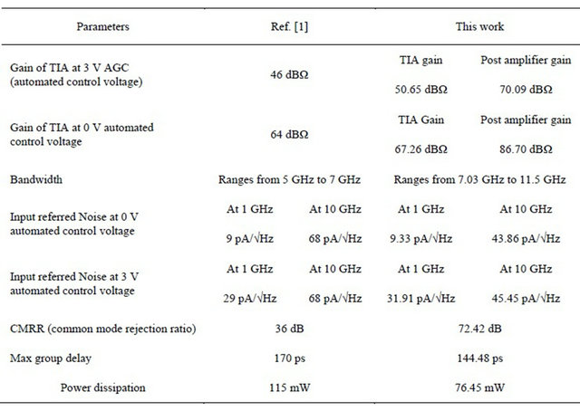
This paper reports design of a CMOS optical receiver front-end using 0.18 μm technology. Design process is current associated with photodiode using trans-impedance amplifier (TIA) for wide bandwidth, high gain, low input referred noise and wide dynamic range. The Automated Gain Control (AGC) voltage is used to provide variable gain for multilevel signals. This design is simulated in 0.18 μm UMC technology for the performance analysis. The best simulation results are reported the maximum TIA gain of 67.26 dBΩ at 0 V AGC followed by a post amplifier gain of 86.70 dBΩ. The bandwidth range is 7.03 GHz to 11.5 GHz corresponding to 0 - 3 V AGC respectively. The input referred noise level value is 43.86 pA/√Hz up to 10 GHz frequency. In addition authors have obtained the common mode rejection ratio (CMRR) is 72.42 dB and rectified group delay is 144.48 ps. Verification of the design, reported results are compared with earlier published work and improvements obtained in the present results.
1. Introduction
Optical receivers find applications in laptop computers, cellular phones, digital cameras, computer peripherals, personal digital assistants (PDAs), and many other consumer electronics equipped with a short-distance communication port. A commonly used topology is the transimpedance (TIA) amplifier, whose relative low input impedance and wide bandwidth is well suited for the application [1]. A wide dynamic range is required for infrared wireless optical receivers in order to accommodate variable link distances, 0 ~ 100 cm. In the design of fixed-gain trans-impedance feedback amplifiers for infrared wireless receivers, there is a direct trade-off between input noise current and the input current overload level via the value of the shunt feedback resistor employed. Therefore, in order to enlarge the dynamic range, various means have been adopted to vary the gain of the trans-impedance amplifiers in response to the input signal levels. Variable-gain trans-impedance feedback amplifiers, however, are prone to instability [2]. TIA needs an Automated Gain Control (AGC) circuit to control the gain of the TIA in order to keep the different symbol levels equally spaced for multilevel signaling [3]. The TIA uses an AC coupled, differential version of the low-voltage topology outlined in [4], which is modified common-gate architecture. It is AC coupled to the photo detector (PD) using vertical parallel plate interconnects capacitors. Figure 1 shows the block representation of the receiver.
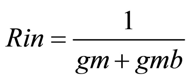
For open loop TIA the input resistance of this amplifier can be determined by [5]:
 (1)
(1)
whererds_1 = the drain to source resistance gm_1 = the device trans-conductance Rd = the drain resistance and gmb_1 = the back-gate trans-conductance due to the body effect For long channel devices operating in the saturation region, the value of rds is large and it can be reduced by this relation:
 (2)
(2)
This is an important result because the bandwidth is independent of the trans-impedance gain set by RD. The unfortunate downside of open loop TIA is that the noise current produced by the load resistance RD and the bias transistor are directly referred to the input with a unity factor therefore closed loop TIA are more preferable because the feedback resistor can be increased independently to the supply voltage since no bias current flows through it. The trans-impedance gain of an ideal inverting voltage amplifier with a feedback resistor Rfb can be given as [1]:
 (3)
(3)
whereA = the open loop voltage gain of the amplifier.
Cpd = the photodiode capacitance.
If the voltages gain “A” of the amplifier is sufficiently high; the trans-impedance is approximately equal to Rfb in the amplifier’s pass band. Assuming that the dominant pole is at the input, the 3db bandwidth of this circuit will be given by the following expression as:
 (4)
(4)
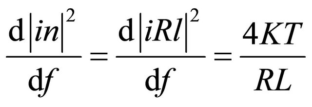
From Equation (4) it can be concluded that the bandwidth of the TIA is greater than that of a simple resistive network by a factor of A + 1. To reduce input referred noise current, TIA uses cascode noise from the resistor is directly referred to the input such that the mean squared input referred noise current spectral density is constant and given in equation
 (5)
(5)
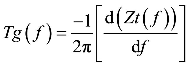
The group delay is defined as the negative of the derivative of the phase of the trans-impedance with respect to frequency [1] common-source topology with feedback resistor. This feedback resistor is implemented to single NMOS transistor in triode operation region because of process variation [6]. The input referred noise current is also dependent on the value of RL. The
 (6)
(6)
A flat group delay means the amplifier has a linear phase response. A flat group delay is important because variations in the group delay with frequency can cause distortions in the output signal.
2. Proposed Design
One of the issues to consider when comparing the two topologies common source and common gate is the effect of the Miller capacitance. Figure 2 shows a small signal equivalent model of the common source (CS) configuration.
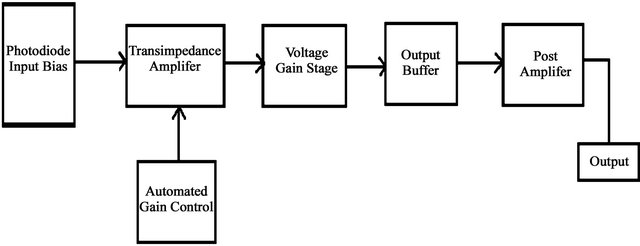
Figure 1. Block diagram of CMOS optical receiver front-end.

Figure 2. Small signal equivalent model of the CS configuration.
The gate to drain capacitance CGD, known as the Miller capacitance, is connected between the input and output. Miller’s theorem allows this capacitance to be replaced with shunt capacitances at the input and output [7]. Miller’s theorem can be derived using Figure 3. Series admittance is connected between two points with a known voltage gain of K. In order to replace this series admittance with shunt admittances the input and the output, the currents I1 and I2 must remain constant during the transformation.
The values of the shunt admittances can now be determined and are shown below.
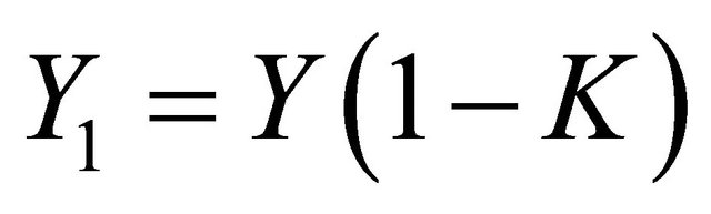 (7)
(7)
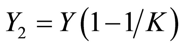 (8)
(8)
This is an interesting result because as the gain is increased, the input capacitance of the amplifier is increased. This reduces the magnitude of the input pole and reduces the bandwidth of the TIA. This effect can be reduced by using the cascode configuration which minimizes the Miller effect by placing a common gate transistor in series with the common source transistor. A voltage gain stage was added after the trans-impedance stage [8]. This stage uses a simple resistive loaded differential pair. Also, for measurement purposes, an output buffer has been added to the TIA. The output buffer is also a resistive loaded differential pair with output impedance that is matched to 50 Ω. The post amplifier is implemented by a fully-differential two-stage operational trans-conductance amplifier [9,10]. Figure 4 shows a schematic view of the proposed design.

Figure 3. Miller theorem equivalent.
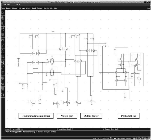
Figure 4. Schematic view of proposed design.
3. Results and Discussions
Figure 5 shows the transient analysis of optical receiver. In this the current at two differential inputs I6 and C1 is converted into the voltage forms using the trans-impedance amplifier. This converted voltage posses no distortion and expressed as the sinusoidal waves at the differential output which is further shifted its level to 3 V at the output of post amplifier.
3.1. AC Analysis
Figure 6 represents the gain of trans-impedance i.e. the ratio of output voltage to input current. At 0 V AGC, the Gain of TIA is 67.26 dBΩ and the corresponding 3 dB bandwidth is 7.03 GHz. This gain is further amplified in this design using post amplifier and amplified gain is 86.70 dBΩ, its graphical representation is given in Figure 7.
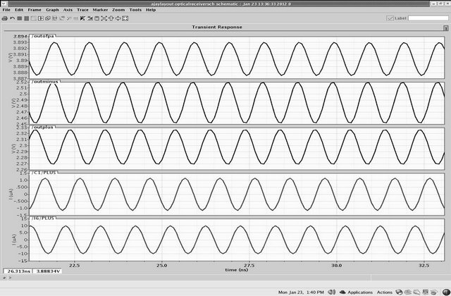
Figure 5. Transient analysis.
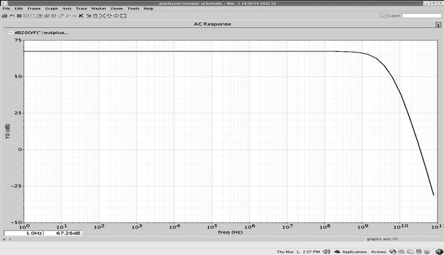
Figure 6. TIA gain at 0 V AGC.
The TIA Gain is 50.65 dBΩ and the corresponding bandwidth is 11.5 GHz at 3 V AGC as shown in Figure 8. This gain is increased to 70.09 dBΩ at the output of the post amplifier as represented in Figure 9" target="_self"> Figure 9 and Phase shift and CMRR of TIA by Figure 10.
3.2. Noise Analysis
From Figure 11, input referred noise is 9.33 pA/√Hz at 0 V AGC pointed to 1 GHz frequency and it is estimated to its lower value of 43.86 pA/√Hz up to 10 GHz frequency. At 3 V/1 GHz AGC the input referred noise is 31.91 pA/√Hz which exceeds its value to 45.45 pA/√Hz upto 10 GHz i.e. the better input noise response as shown in Figure 12.
3.3. Group Delay
Figure 13 prescribed that the group delay is 144.48 ps and is maintained constant till 1 GHz frequency and afterwards starts decaying for the higher range of frequencies. Table 1 presents the comparison of present results with earlier published work.
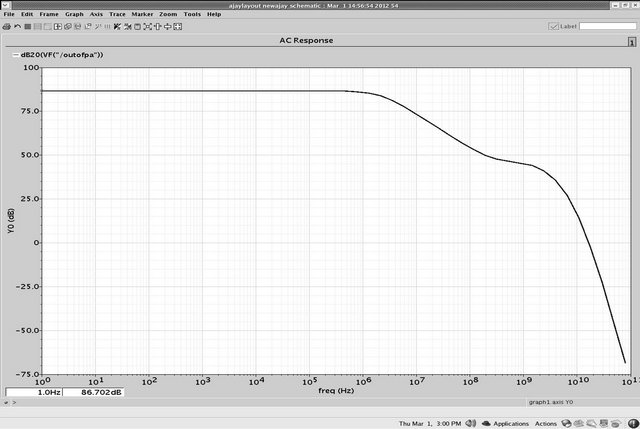
Figure 7. Post amplifier gain at 0 V AGC.

Figure 8. TIA gain at 3 V AGC.

Figure 9. Post amplifier gain at 3 V AGC.
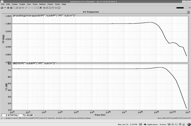
Figure 10. Phase shift and CMRR of TIA.

Figure 11. Input referred noise response at 0 V AGC.
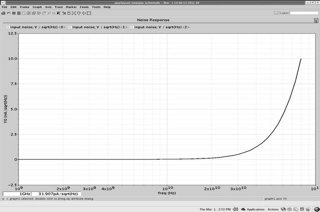
Figure 12. Input referred noise response at 3 V AGC.

Figure 13. Group delay response.
4. Conclusion
This paper presents a design of an optical receiver that enables to receive the light signals with the help of photodiode. This photodiode thus convert these signals into electric current and current to voltage conversion occurs at TIA gain stage. The TIA is able to generate variable gain ranging from 50.65 dBΩ to 67.26 dBΩ at 0 - 3 V AGC voltage. This gain can further be amplified from 70.09 dBΩ to 86.70 dBΩ using post amplifier which has improved gain value as compare to earlier reported work as given in Table 1. From this table it is clear that this work provide high bandwidth of 11.5 GHz and lower input referred noise value of 43.86 pA/√Hz up to 10 GHz frequency. The design has average power dissipation of 76.45 mW with a group delay of 144.48 ps. The
Table 1. Comparison of present results with earlier published work.
simulation results show wide bandwidth, high gain and lower input referred noise, low power dissipation which is suitable in laptop computers, cellular phones, digital cameras, computer peripherals.
5. Acknowledgements
This work has been carried out in SMDP VLSI laboratory of the Electronics and Instrumentation Engineering department of Shri G. S. Institute of Technology and Science, Indore, (M. P.) India. This SMDP VLSI project is funded by Ministry of Information and Communication Technology, Government of India. Authors are thankful to the Ministry for the facilities provided under this project.
REFERENCES
- R. D. Bespalko, “Transimpedance Amplifier Design Using 0.18 μm CMOS Technology,” Queen’s University Kingston, Ontario, 2007.
- R. Y. Chen, T. S. Hung and C. Y. Hung, “A CMOS Infrared Wireless Optical Receiver Front-End with a Variable-Gain Fully-Differential Transimpedance Amplifier,” IEEE Transactions on Consumer Electronics, Vol. 51, No. 2, 2005, pp. 424-429. doi:10.1109/TCE.2005.1467982
- S. Hranilovic and D. A. Johns, “A Multilevel Modulation Scheme for High-Speed Wireless Infrared Communications,” Proceedings of IEEE International Symposium on Circuits and Systems (ISCAS), Vol. 6, 1999, pp. 338-341.
- D. Guckenberger, J. Schaub and K. Komegay, “A DC Coupled Low-Power Transimpedance Amplifier Architecture for Gb/s Communication System Applications,” Design of Radio Frequency Integrated Circuit (RFIC) Symposium, June 2004, pp. 515-518.
- B. Razavi, “Design of Integrated Circuits for Optical Communications,” McGraw Hill, Boston, 2003.
- C. Ciofietal, “A New-Circuit Topology for the Realization of Very Low-Noise Wide-Bandwidth Trans-Impedance Amplifier,” IEEE Transactions on Instrument and Measurement, Vol. 56, No. 5, 2007, pp. 1626-1631.
- A. S. Sedra and K. C. Smith, “Microelectronic Circuits,” 4th Edition, Oxford University Press, New York, 1998.
- A. Phillip and D. R. Holberg, “CMOS Analog Circuit Design,” 2nd Edition, Oxford University Press, New York, 2003.
- F. T. Chien and Y. J. Chan, “Bandwidth Enhancement of Transimpedance Amplifier by a Capacitive Peaking Design,” IEEE Journal of Solid State Circuits, Vol. 34, 1999, pp. 1167-1170.
- S. M. Park and H.-J. Yoo, “1.25-Gb/s Regulated Cascade CMOS Transimpedance Amplifier for Gigabit Ethernet Applications,” IEEE Journal of Solid State Circuits, Vol. 39, No. 1, 2004, pp. 112-121. doi:10.1109/JSSC.2003.820884