Optics and Photonics Journal
Vol.2 No.3A(2012), Article ID:23305,4 pages DOI:10.4236/opj.2012.223036
Wave Transmission in Dispersive Si-Based One Dimensional Photonic Crystal
1Department of Physics, Digamber Jain College, Baraut, India
2Department of Physics, Government College of Engineering & Technology, Bikaner, India
3AITTM, Amity University, Noida, India
4Department of Physics, Janta Vedic College, Baraut, India
5Nanophysics Laboratory, Department of Physics, Government Dungar College, Bikaner, India
6IIMT, Greater Noida, India
Email: *vrpcommon@gmail.com
Received June 14, 2012; revised July 15, 2012; accepted July 25, 2012
Keywords: Photonic Crystals; Omni-Directional Reflection; Optical Filter
ABSTRACT
Transmission of electromagnetic waves through a Si-based one dimensional photonic crystal has been investigated. The proposed structure works as an omni-directional reflector for a certain range of wavelength for an angle of incidence up to 55˚. The structure works as a narrow band TM-polarization filter for an angle of incidence more than 55˚, i.e. a filter which completely blocks TE-polarized waves but allows certain wavelengths of TM-polarized waves. But at an angle of incidence of 89˚, the structure works as a multiple narrow band TM-polarization filter even though no defect layer is introduced inside the structure. It is also found that this multiple narrow pass-bands of TM-polarized waves can be tuned to a desired range of wavelength by changing the temperature of the structure.
1. Introduction
Since the pioneering works of Yablonovitch and John, the studies on the electromagnetic properties of photonic crystals (PCs) which are artificial structures with periodically modulated dielectric constants has been attracting a great deal of interest among researchers [1-7]. It was observed that periodic modulation of the dielectric functions significantly modifies the spectral properties of the electromagnetic waves. The electromagnetic spectrum in such structures is characterized by the presence of allowed and forbidden photonic energy bands similar to the electronic band structure of periodic potentials. For this reason, such a new class of artificial optical material with periodic dielectric modulation is known as photonic band gap (PBG) material [8]. Fundamental optical properties like band structure, reflectance, group velocity and rate of spontaneous emission, etc. can be controlled effectively by changing the spatial distribution of the dielectric function [4,5].
A 1-D PC structure has many interesting applications such as dielectric reflecting mirrors, low-loss waveguides, optical switches, filters, optical limiters etc. It has also been demonstrated theoretically and experimentally that 1-D PCs may exhibit absolute omni-directional PBGs [9-13]. In addition to the existence of wide photonic band gaps in some properly designed PCs, the feature of a tunability of PBGs in PCs attracts the attention of investigators in recent years. PBGs can be tuned by means of some external agents. For instance, band-gaps can be shifted by changing the operating temperature and it is generally known as the T-tuning. A superconductor/dielectric PC belongs to this type of photonic crystals. This happens because of the temperature-dependent London perturbation length in the superconducting materials [14-17].
However, in earlier reports the dielectric media taken by the researchers were considered to be independent of temperature and non-dispersive. In the present communication, we consider semiconductor media as one of the constituents of a one dimensional photonic crystal, since the dielectric property of semiconductors depends not only on temperature but also on wavelength. Here, we consider a Si/air multilayer system. The refractive index of air is independent of temperature and wavelength. But the refractive index of silicon layer can be taken as a function of temperature and wavelength both [18]. Therefore, this study may be considered to be more physically realistic.
2. Theoretical Analysis
The schematic representation of one-dimensional photonic crystal is shown in Figure 1. We consider air/(AB) NA/air structure in which A and B represent the high and low refractive index materials. To compute the transmission spectrum, we employ the transfer matrix method (TMM) [19].
In TMM method, the transfer matrix for each layer can be written as
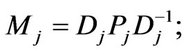 (1)
(1)
where, j stands for A or B layers and Dj and Pj are called the dynamical matrix and the propagation matrix respectively. The dynamical matrix is given by the following equations
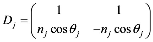 for TE mode (2)
and
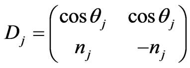 for TM mode (3)
Also, the propagation matrix Pj can be defined as
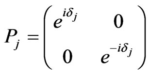 (4)
(4)
where the phase is written as
 (5)
(5)
The transfer matrix, for the structure embedded in air, the transfer matrix for the air/(AB)NAN/air structure can be written as
 (6)
(6)
where, D0 is called the dynamical matrix for air.
The reflection and transmission coefficients in terms of the matrix elements given in Equation (6) can be written as
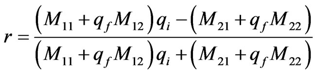 (7)
(7)
and
 (8)
(8)
where 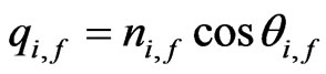 for TE wave and
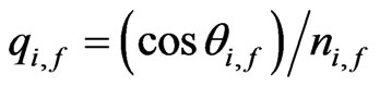
for TM wave, where the subscripts i and f correspond to the quantities respectively in the medium of incidence and the medium of emergence. Whereas, the reflectance and transmittance of the structure is given by
 (9)
(9)
3. Proposed Structure and Structural Parameters
We choose Si for the material A, air for material B and the number of unit cells, N = 10 in Figure 1. So, the proposed structure will be [air/(Si/air)10Si/air]. We take silicon and air as the high and the low refractive index materials respectively. The geometrical parameters are so chosen that the thicknesses of high and low refractive index materials are same at 300 K temperature i.e. d1 = d2 = 500 nm. The thermal expansion coefficient and melting point for silicon layer are 2.6 × 10⁻⁶/K and 1685 K respectively [20]. Also, it is considered that there will be almost negligible expansion in Si layers with the variation of temperature and hence thermal expansion of Si can be safely neglected as compared to the dimensions considered here. The refractive index of air is independent of temperature and wavelength. But the refractive index of silicon layer is taken as a function of both wavelength and temperature. The refractive index of Silicon (Si) in the ranges 1.2 to 14 μm and 20 - 1600 K is represented as [18]
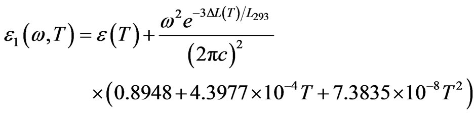 (10)
(10)
where

and 

Figure 1. Schematic diagram of 1-D photonic crystal structure.
for 20 K ≤ T ≤ 293 K
for 293 K ≤ T ≤ 1600 K.
4. Results and Discussion
In this section, we present discussion on the transmission spectra of the proposed structure. By computing Equation (9) for TE and TM modes of polarization in one dimensional photonic crystal, we plotted the transmittance of the structure as a function of wavelength. Also, the plot of the refractive index as the function of wavelength and temperature is shown in Figure 2. From Figure 2, it is clear that the refractive index of silicon layer decreases with the increase in wavelength and increases with increase in temperature. The rate of increase in refractive index with temperature is 0.02/100 K and the rate of decrease in refractive index with wavelength is 0.001/μm. Therefore, the overall refractive index contrast of the alternate layers of the structure will increase if the change in temperature of the structure is properly adjusted for certain change in wavelength.
The transmission spectra of the proposed structure for TE and TM polarizations at 300 K are plotted in Figure 3. We choose three different angles of incidence to be at 0˚,

Figure 2. Variation of refractive index (a) with temperature at constant wavelength; (b) with wavelength at constant temperature.

Figure 3. Transmission spectra for TE (solid) and TM-polarization (dashed) at 300 K.
30˚ and 55˚ respectively. We observe from these Figures that the TE polarization has its omni-directional reflection range from 3.76 μm to 6.10 μm and the omnidirectional reflection range for the TM polarization is from 3.76 μm to 4.36 μm for the angles of incidence from 0˚ to 55˚. Therefore, the range for which both the TE and TM polarizations exhibit omni-directional reflection (ODR) has the bandwidth (∆λ = λH – λL) of 0.60 μm for this range of the angle of incidence. This ODR range can be tuned by varying the temperature of the structure.
The transmission spectra at 89˚ for the both polarizations are shown in Figure 4. For the angle of incidence more than 55˚, we found that the ODR range of TE polarization is nearly the same as in the case of angle of incidence at 55˚ or less. But for the angle of incidence greater than 55˚, the TM polarization does not exhibit ODR region. So, for angles of incidence more than 55˚, the structure works as a multiple narrow band TM-polarization filter i.e. a filter which completely blocks the TE-polarized wave but allows certain extremely narrow bands or peaks of wavelengths of the TM-polarized wave to be transmitted through the structure [21]. Particularly at an angle of incidence of 89˚, a few sharp transmission peaks are found in the transmission spectra rather. So, at the angle of incidence of 89˚, the structure works as a multi-channel optical filter even without introducing any defect in the geometry [17]. From Figure 4(b), it is also clear that if we increase the temperature of the structure, the transmission peaks shift towards the higher wavelength region.
This shifting behavior of transmission peaks can be explained by using the phase Equation (5). According to this phase equation, as refractive index of the Si layer in R.H.S. increase with temperature, the wavelength must increase accordingly to keep the phase (L.H.S.) unchanged. The shifting of transmission peaks of TM polarization, which lie in the forbidden region of the TE polarization, is shown in Figure 5. The variation of central wavelength of first transmission peak with temperature is shown in Figure 6. It is found that the central wavelength of transmission peak changes approximately

Figure 4. Transmission spectra for (a) TE-polarization at 300 K; (b) TM-polarization at 300 K (solid line) and 900 K (dotted line).

Figure 5. Shifting of transmission peaks with temperature for TM-polarization at 89˚ (solid line for 300 K and dotted line for 900 K).
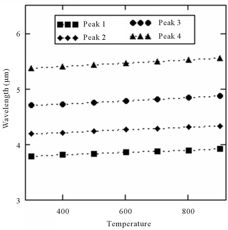
Figure 6. Variation of central wavelength of first transmission peak (TM-polarization) with temperature at 89˚.
linearly with temperature. Thus, the first transmission peak which are at 3.78 μm at 300 K are shifted to 3.92 μm at 900 K. So, we can tune the transmission peaks at desired wavelength by changing the temperature of the structure.
5. Conclusion
The proposed structure works as omni-directional reflector for an angle of incidence on the structure up to 55˚. For higher angles of incidence the structure works as a selective multiple narrow band TM-polarization filters. Also, at the angle of incidence of 89˚, the structure works as a multi-channel optical filter even without introducing any defect in the geometry. Such a structure can be used as temperature sensing device, narrow band optical filter and in many optical systems.
REFERENCES
- E. Yablonovitch, “Inhibited Spontaneous Emission in Solid-State Physics and Electronics,” Physical Review Letters, Vol. 58, No. 20, 1987, pp. 2059-2062. doi:10.1103/PhysRevLett.58.2059
- K. M. Ho, C. T. Chan and C. M. Soukoulis, “Existence of a Photonic Gap in Periodic Dielectric Structures,” Physical Review Letters, Vol. 65, No. 25, 1990, pp. 3152-3155. doi:10.1103/PhysRevLett.65.3152
- J. D. Joannopoulos, P. Villeneuve and S. Fan, “Photonic Crystals: Putting a New Twist on Light,” Nature, Vol. 386, No. 6621, 1997, pp. 143-149. doi:10.1038/386143a0
- J. A. M. Rojas, J. Alpuente, J. Pineiro and R. Sanchez, “Rigorous Full Vectorial Analysis of Electromagnetic Wave Propagation in 1d Inhomogeneous Media,” Progress in Electromagnetics Research, Vol. 63, 2006, pp. 89-105. doi:10.2528/PIER06042501
- E. Yablonovitch and T. J. Gmitter, “Photonic Band Structure: The Face-Centered-Cubic Case,” Physical Review Letters, Vol. 63, No. 18, 1989, pp. 1950-1953. doi:10.1103/PhysRevLett.63.1950
- J. D. Joannopoulos, R. D. Meade and J. N. Winn, “Photonic Crystals: Molding the Flow of Light,” Princeton University Press, Princeton, 1995.
- E. Burstein and C. Weisbuch, “Confined Electron and Photon: New Physics and Applications,” Plenum Press, New York, 1995. doi:10.1007/978-1-4615-1963-8
- C. M. Soukoulis, “Photonic Band Gap Materials,” Kluwer Academic, Dordrecht, 1996. doi:10.1007/978-94-009-1665-4
- J. P. Dowling, “Mirror on the Wall: You’re Omnidirectional after All?” Science, Vol. 282, No. 5395, 1998, pp. 1841- 1842. doi:10.1126/science.282.5395.1841
- E. Yablonovitch, “Engineered Omnidirectional ExternalReflectivity Spectra from One-Dimensional Layered Interference Filters,” Optics Letters, Vol. 23, No. 21, 1998, pp. 1648-1649. doi:10.1364/OL.23.001648
- D. N. Chigrin, A. V. Lavrinenko, D. A. Yarotsky and S. V. Aponenko, “Observation of Total Omnidirectional Reflection from a One Dimensional Dielectric Lattice,” Applied Physics A: Materials Science & Processing, Vol. 68, No. 1, 1999, pp. 25-28. doi:10.1007/s003390050849
- B. Suthar, V. Kumar, Kh. S. Singh and A. Bhargava, “Tuning of Photonic Band Gaps in One Dimensional Chalcogenide Based Photonic Crystal,” Optics Communications, Vol. 285, No. 6, 2012, pp. 1505-1509. doi:10.1016/j.optcom.2011.10.047
- V. Kumar, Kh. S. Singh, S. K. Singh and S. P. Ojha, “Broadening of Omnidirectional Photonic Band Gap in Si-Based One Dimensional Photonic Crystals,” Progress in Electromagnetics Research M, Vol. 14, 2010, pp. 101- 111. doi:10.2528/PIERM10062807
- O. L. Bermann, Y. E. Lozovik, S. L. Eiderman and R. D. Coalson, “Superconducting Photonic Crystals: Numerical Calculations of the Band Structure,” Physical Review B, Vol. 74, No. 9, 2006, Article ID: 092505. doi:10.1103/PhysRevB.74.092505
- H. Takeda and K. Yoshino, “Tunable Photonic Band Schemes in Two-Dimensional Photonic Crystals Composed of Copper Oxide High-Temperature Superconductors,” Physical Review B, Vol. 67, No. 24, 2005, Article ID: 245109. doi:10.1103/PhysRevB.67.245109
- W.-H. Lin, C.-J. Wu, T.-J. Yang and S.-J. Chang, “Terahertz Multichanneled Filter in a Superconducting Photonic Crystal,” Optics Express, Vol. 18, No. 26, 2010, Article ID: 27155. doi:10.1364/OE.18.027155
- M.-S. Chen, C.-J. Wu and T.-J. Yang, “Investigation of Optical Properties in Near-Zero-Permittivity Operation Range for a Superconducting Photonic Crystal,” Applied Physics A: Materials Science & Processing, Vol. 104, No. 3, 2011, pp. 913-919. doi:10.1007/s00339-011-6439-4
- H. H. Li, “Refractive Index of Silicon and Germanium and Its Wavelength and Temperature Derivatives,” Journal of Physical and Chemical Reference Data, Vol. 9, No. 3, 1980, p. 561. doi:10.1063/1.555624
- P. Yeh, “Optical Waves in Layered Media,” John Wiley and Sons, New York, 1988.
- G. Ghosh, “Handbook of Thermo-Optic Coefficients of Optical Materials with Applications,” Academic Press, New York, 1985.
- S. K. Awasthi, A. Mishra, U. Malaviya and S. P. Ojha, “Wave Propagation in a One-Dimensional Photonic Crystal with Metamaterial,” Solid State Communications, Vol. 149, No. 33-34, 2009, pp. 1379-1383. doi:10.1016/j.ssc.2009.05.017
NOTES
*Corresponding author.