 New Journal of Glass and Ceramics, 2011, 1, 69-78 doi:10.4236/njgc.2011.12012 Published Online July 2011 (http://www.SciRP.org/journal/njgc) Copyright © 2011 SciRes. NGJC Physical Study of Thin Film and Monolithic Nano-Composites [SiO2:11P2O5:3Al2O3:(1.2)Er (1.2, 1.8 and 3)Yb] Prepared by Sol Gel Technique, Planar Waveguide and Co-operative Up-Conversion Y. Badr1, I. K. Battisha2, A. M. S. El Nahrawy2, M. Kamal3 1National Institute of Laser Enhancement Sciences (NILES), Cairo University, Cairo, Egypt; 2National Research Center (NRC) Department of Solid State Physics, Doki, Giza, Egypt; 3Physics Department El Manssoura University, Egypt. Email: szbasha@yahoo.com Received May 21st, 2011; Revised June 18th, 2011; Accepted June 25th, 2011. ABSTRACT Nano-composite silica-phosphate system (SiO2-P2O5) co-doped with Al2O3 as a host material and prepared by sol gel technique in two forms monolith and thin film using multilayer spin-coating method were activated by Er3+ and Yb3+ ions as in the formula; [SiO2:11P2O5:3Al2O3:(1.2)Er:(1.2, 1.8 and 3)Yb]. The prepared samples have been synthesized using tetra-ethyl-o rthosilicate (TEOS) and trieth yl-phosphate (TEP) as precursor sources o f silica and phosphorus ox- ides. The microstructure and crystallinity of the prepared samples will be characterized by using x-ray diffraction (XRD) which, imply that the crystallite sizes of [SiO2:11P2O5:3Al2O3:(1.2)Er:(1.2) Yb] at 500℃ for bo th thin fi lm and monolith forms of the prepared samples were found to be equal to 35 and 33 nm, respectively. The refractive index will be evaluated by measuring the normal transmission and specular reflection of the prepared samples. The photo- luminescen ce prop erties ha ve ana lyzed in the visible waveleng th rang e between 500 and 800 nm a s a function o f sam- ple composition. Keywords: Sol-Gel, Silica-Phosphate, Rare Earth, XRD, Photoluminescence, Waveguide, Co-Operative Up-Conversion 1. Introduction In the last decade, various technologies have been em- ployed for the fabrication of silica (SiO2) based inte- grated optics (IO) components and a broad variety of silicate glass systems have been investigated. So sil- ica-phosphate glasses doped with rare earth have been favored in the development of integrated waveguide am- plifiers, where the rare-earth concentration must be or- ders of magnitude higher than in fibers [1]. Glasses syn- thesized by the sol–gel method are promising matrices for the formation of optical nano-composites. The use of these nano-composites in optoelectronics, photonics and fiber optics has opened up the new way for the develop- ment of unique information systems with tunable char- acteristics over a wide frequency range [2]. Sol-gel processing, has been shown to be a relatively inexpen- sive method to prepare such IO components [3,4], which may allow the incorporation of RE ion concentrations higher than those possible by conventional glass melting methods, but at the same time the stronger ion-ion inter- actions may reduce the RE fluorescence performance, by decreasing its intensity and lifetime. Photonic materials for optical amplifiers’ based on rare-earth (RE) ions such as Er3+, are in wide use today, especially for dense wavelength division multiplexing (DWDM) applications. However, the small absorption cross sections of Er3+ ions have become a limitation to the optimization of such materials for optical amplification and, therefore, a number of methods have been proposed to increase the excitation efficiency of Er3+ ions [5]. It was previously reported that, the wavelength of the main Er3+ ground- state transition, 1.54 µm, coincides with the standard wave- 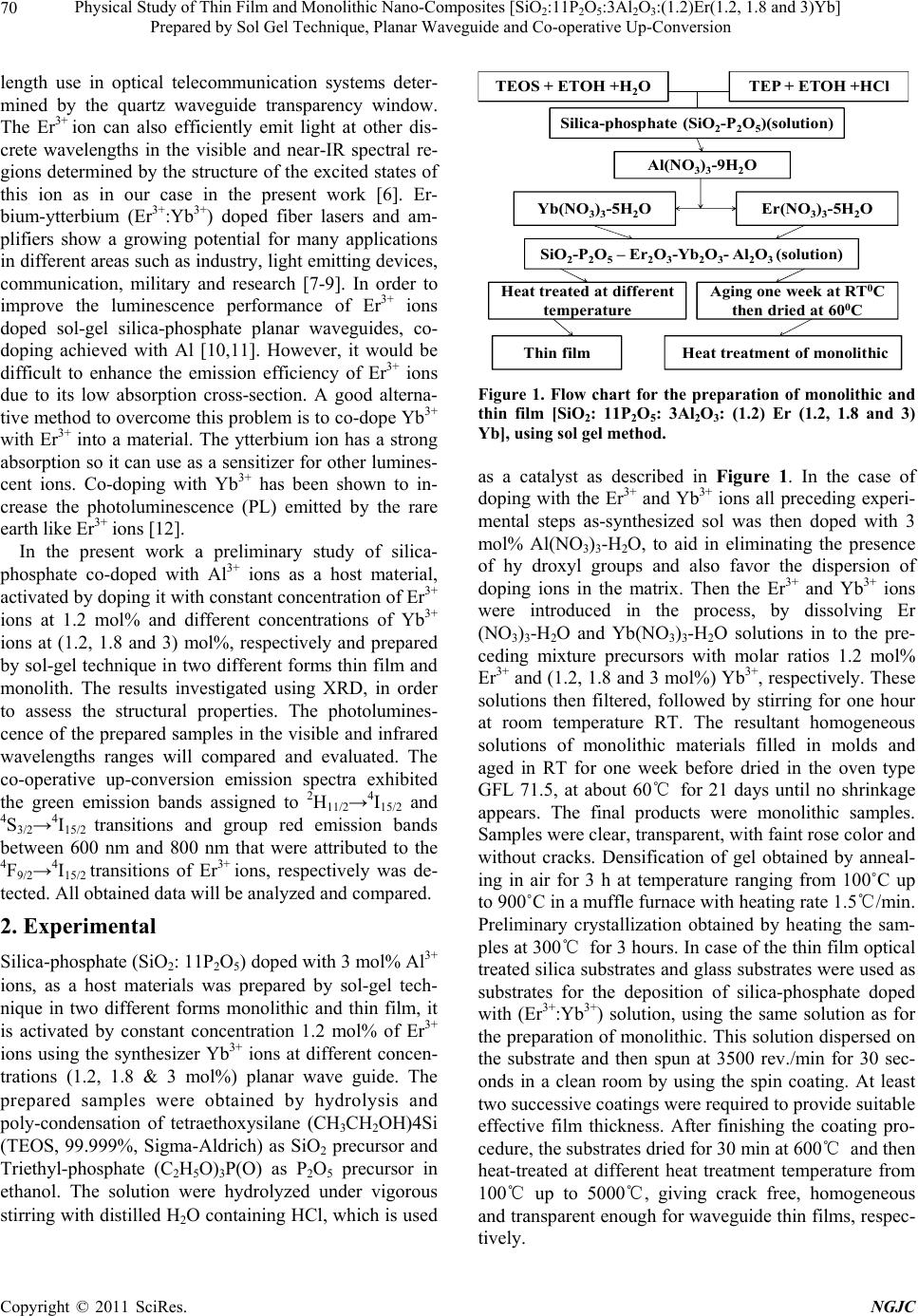 Physical Study of Thin Film and Monolithic Nano-Composites [SiO:11P O:3Al O:(1.2)Er(1.2, 1.8 and 3)Yb] 70 22 523 Prepared by Sol Gel Technique, Planar Waveguide and Co-operative Up-Conversion length use in optical telecommunication systems deter- mined by the quartz waveguide transparency window. The Er3+ ion can also efficiently emit light at other dis- crete wavelengths in the visible and near-IR spectral re- gions determined by the structure of the excited states of this ion as in our case in the present work [6]. Er- bium-ytterbium (Er3+:Yb3+) doped fiber lasers and am- plifiers show a growing potential for many applications in different areas such as industry, light emitting devices, communication, military and research [7-9]. In order to improve the luminescence performance of Er3+ ions doped sol-gel silica-phosphate planar waveguides, co- doping achieved with Al [10,11]. However, it would be difficult to enhance the emission efficiency of Er3+ ions due to its low absorption cross-section. A good alterna- tive method to overcome this problem is to co-dope Yb3+ with Er3+ into a material. The ytterbium ion has a strong absorption so it can use as a sensitizer for other lumines- cent ions. Co-doping with Yb3+ has been shown to in- crease the photoluminescence (PL) emitted by the rare earth like Er3+ ions [12]. In the present work a preliminary study of silica- phosphate co-doped with Al3+ ions as a host material, activated by doping it with constant concentration of Er3+ ions at 1.2 mol% and different concentrations of Yb3+ ions at (1.2, 1.8 and 3) mol%, respectively and prepared by sol-gel technique in two different forms thin film and monolith. The results investigated using XRD, in order to assess the structural properties. The photolumines- cence of the prepared samples in the visible and infrared wavelengths ranges will compared and evaluated. The co-operative up-conversion emission spectra exhibited the green emission bands assigned to 2H11/2→4I15/2 and 4S3/2→4I15/2 transitions and group red emission bands between 600 nm and 800 nm that were attributed to the 4F9/2→4I15/2 transitions of Er3+ ions, respectively was de- tected. All obtained data will be analyzed and compared. 2. Experimental Silica-phosphate (SiO2: 11P2O5) doped with 3 mol% Al3+ ions, as a host materials was prepared by sol-gel tech- nique in two different forms monolithic and thin film, it is activated by constant concentration 1.2 mol% of Er3+ ions using the synthesizer Yb3+ ions at different concen- trations (1.2, 1.8 & 3 mol%) planar wave guide. The prepared samples were obtained by hydrolysis and poly-condensation of tetraethoxysilane (CH3CH2OH)4Si (TEOS, 99.999%, Sigma-Aldrich) as SiO2 precursor and Triethyl-phosphate (C2H5O)3P(O) as P2O5 precursor in ethanol. The solution were hydrolyzed under vigorous stirring with distilled H2O containing HCl, which is used TEP + ETOH +HClTEOS + ETOH +H 2 O Silica-phosphate (SiO 2 -P 2 O 5 )(solution) Yb(NO 3 ) 3 -5H 2 O Al(NO 3 ) 3 -9H 2 O SiO 2 -P 2 O 5 –Er 2 O 3 -Yb 2 O 3 -Al 2 O 3 (solution) Aging one week at RT 0 C then dried at 60 0 C Heat treatment of monolithic Er(NO 3 ) 3 -5H 2 O Heat treated at different temperature Thin film Figure 1. Flow chart for the preparation of monolithic and thin film [SiO2: 11P2O5: 3Al2O3: (1.2) Er (1.2, 1.8 and 3) Yb], using sol gel method. as a catalyst as described in Figure 1. In the case of doping with the Er3+ and Yb3+ ions all preceding experi- mental steps as-synthesized sol was then doped with 3 mol% Al(NO3)3-H2O, to aid in eliminating the presence of hy droxyl groups and also favor the dispersion of doping ions in the matrix. Then the Er3+ and Yb3+ ions were introduced in the process, by dissolving Er (NO3)3-H2O and Yb(NO3)3-H2O solutions in to the pre- ceding mixture precursors with molar ratios 1.2 mol% Er3+ and (1.2, 1.8 and 3 mol%) Yb3+, respectively. These solutions then filtered, followed by stirring for one hour at room temperature RT. The resultant homogeneous solutions of monolithic materials filled in molds and aged in RT for one week before dried in the oven type GFL 71.5, at about 60℃ for 21 days until no shrinkage appears. The final products were monolithic samples. Samples were clear, transparent, with faint rose color and without cracks. Densification of gel obtained by anneal- ing in air for 3 h at temperature ranging from 100˚C up to 900˚C in a muffle furnace with heating rate 1.5℃/min. Preliminary crystallization obtained by heating the sam- ples at 300℃ for 3 hours. In case of the thin film optical treated silica substrates and glass substrates were used as substrates for the deposition of silica-phosphate doped with (Er3+:Yb3+) solution, using the same solution as for the preparation of monolithic. This solution dispersed on the substrate and then spun at 3500 rev./min for 30 sec- onds in a clean room by using the spin coating. At least two successive coatings were required to provide suitable effective film thickness. After finishing the coating pro- cedure, the substrates dried for 30 min at 600℃ and then heat-treated at different heat treatment temperature from 100℃ up to 5000℃, giving crack free, homogeneous and transparent enough for waveguide thin films, respec- tively. C opyright © 2011 SciRes. NGJC  Physical Study of Thin Film and Monolithic Nano-Composites [SiO2:11P2O5:3Al2O3:(1.2)Er(1.2, 1.8 and 3)Yb] Prepared by Sol Gel Technique, Planar Waveguide and Co-operative Up-Conversion Copyright © 2011 SciRes. NGJC 71 X-ray diffraction (XRD) patterns from the prepared samples were recorded with Philips X-ray diffractometer PW/1710; with Ni filter, with monochromatised CuK radiation of wavelength 1.54045 Å at 40 KV and 30 mA. Crystallite sizes G were determined from the Scherrer’s equation (G = K /Dcos ), where is the wavelength, and D is the (corrected) full width (in radians) of the peak at half maximum (FWHM) intensity. The correction to the measured FWHM Ds for a sample peak was made to accommodate systematic in- strumental broadening and utilized peak widths Dq measured from a diffraction scan, taken under identical conditions, from a strain-free powdered quartz sample, with crystallite size ranging between 5 and 10 lm. The corrected sample peak widths were calculated as (D = Ds2 – Dk2)1/2 Micro-strain and crystallite size contributions to D separated using the Win-Fit program, using standard samples for estimation of instrumental broadening. The final sample crystallite sizes G obtained by Fourier analysis, using the corrected profile. Nearly normal transmittance and reflectance spectra were done by Jasco V-570 spectrophotometer, in wavelength range (0.2 - 2.5 µm). The transmission electron microscope (TEM) al- lows the user to determine the internal structure of mate- rials. TEM was performed by using a JEOL JEM-1230 operating at 120 KV attached to CCD camera. For photoluminescence (PL) measurement, the sample excited by the 488 nm line of a Spectra Physics 2017 Argon laser used to excite room temperature lumines- cence spectra. A fiber optic probe coupled to a Dilor Su- perhead, equipped with a suitable notch filter, employed. The scattered signal analyzed by a Jobin-Yvon HR 460 mono-chromator and a spectrum one CCD detector. A 150 line/mm grating used to collect the laser-excited luminescence spectra, whilst for high-resolution lumi- nescence spectra a 1200 lines/mm grating employed. The PL emission obtained using lock-in amplifier (SR 510- Stanford) technique and recorded by computer. The measurements performed at room temperature. 3. Results and Discussion 3.1. XRD Results Figures 2 and 3 show the XRD patterns of mono- lithic(SiO2:11P2O5:3Al2O3:1.2Er2O3) doped with dif- ferent concentrations of Yb3+ ions as in the formula(SiO2: 11P2O5:3Al2O3:(1.2)Er(1.2, 1.8 and 3)Yb), sintered at different heat treatment temperatures (100˚C, 300˚C and 10 20 30 40 50 60 70 80 (A ) abc 10 20 30 40 50 60 70 80 pp p c b (B) 20 SiP2O7 Si5P6O25 p Si3(PO4)4 . * * * p * * . . . . a Intensity (a .u.) Figure 2 (A, B). XRD patterns of monolithic SiO2:11P2O5:3Al2O3 doped with (a) 1.2Er3+:1.2Yb3+ (b) 1.2Er3+:1.8Yb3+and (c) 1.2Er3+:3Yb3+, sintered at (A) 100˚C and (B) 300˚C for 3 h; p Si3(PO4)4 phase, * Si5P6O25 phase and • SiP2O7 phase. Figure 3 (a, b and c). XRD patterns of monolithic SiO2:11P2O5:3Al2O3 doped with (a) 1.2 Er3+:1.2Yb3+ (b) 1.2Er3+:1.8Yb3+ nd (c) 1.2Er3+: 3Yb3+, sintered at 700˚C for 3 h; p Si3(PO4)4 phase, * Si5P6O25 phase, ∆ Er3SiPO9 phase and • SiP2O7phase. a  Physical Study of Thin Film and Monolithic Nano-Composites [SiO:11P O:3Al O:(1.2)Er(1.2, 1.8 and 3)Yb] 72 22 523 Prepared by Sol Gel Technique, Planar Waveguide and Co-operative Up-Conversion 700˚C) for 3 h. When silica-phosphate doped with (Er3+: Yb3+) ions subjected to heat treatment for densification, many properties of the gel changed as a result of struc- tural changes in the host skeleton of a gel which, is at- tributed to the development of cross-linking of the Si-O and P-O bonds due to dehydration poly- condensation of the system. The curves sintered at 100˚C show broad hump at 2 between 18˚ and 30˚ attributed to amorphous matrix. By increasing the temperature up to 300˚C very weak peaks of silica-phosphate begin to appear due to the presence of silica-phosphate nanocompounds. As- signed to (hexagonal silica phosphate) Si3(PO4)4 and (rhombohedra silica phosphate) Si5P6O25 phases accord- ing to JCPDS cards- number (22 - 1380) and (70 - 2071). These phases consists of isolated SiO6 and Si2O7 units linked by PO4 groups in the system silica-phosphate [13-15] to form SiO2-P2O5 nano- composite [16,17] in addition of the presence of monoclinic silica phosphate (SiP2O7) phase according to JCPDS card number (71 - 2073). Above 300˚C, the crystallization in silica-pho- sphate gel glasses greatly changed the coordination of Er3+:Yb3+ ions. An Er3+:Yb3+ ions situated in a binary system composed of crystalline and glass phase. Another effect of increasing the temperature of the samples is that the intensity of the XRD peaks increased due to the con- tinually change in the chemical structure and the rear- rangements of the crystalline system. Then the prepared samples become crystalline, with separation of the phases; according to the diffraction peaks as shown in Figure 3. By increasing the sintering temperature up to 700˚C, the intensity of XRD patterns increase giving rise to crystallinity enhancement. Separation of the phases; according to the diffraction peaks, the (hexagonal sil- ica-phosphate) Si3(PO4)4 phase was eliminated by in- creasing the temperature and the (rhombohedra silica phosphate) Si5P6O25, (silica phosphate) SiP2O7 phases increase and a new phase ( monoclinic erbium silica phosphate) Er3SiPO9 appeared due to the effect of the Er3+ ions, according to JCPDS cards no.(49 - 0206). Figures 4 and 5 show the XRD patterns for some thin films silica-phosphate system co-doped 3 mol% Al2O3 with 1.2 mol% Er3+:(1.2 & 1.8)Yb3+ ions samples as in the following formula; (SiO2:11P2O5:3Al2O3:1.2Er2O3: (1.2 & 1.8)Yb2O3) prepared from the same precursors, sintered at different heat treatment temperatures, 100˚C, 150˚C, and 500˚C for 3 h. The behavior of the prepared thin film samples after dried at low sintered temperature 100˚C and 150˚C, give nearly the same trend of the monolithic samples observed where the samples were still in the amorphous state and have larger specific area. By increasing the sintered heat treatment temperature up to 500˚C, the intensities of the Si3(PO4)4, Si5P6O25 and SiP2O7 phases increase with increasing the sintering heat treatment temperature. While, the initial state of a film generally denser and less cross-linked than a bulk gel made from the same sol, and this transport path of heat through the thickness of the film. Where, these films have been prepared from the same precursor of preparing the monolith samples by aging two days after spinning. The observed change in the XRD peaks height as well as the broadening could interpreted by the adsorption of the incorporated atoms on the surface of the growing sil- ica-phosphate doped with REEs gel microcrystal. The thinner of the film thickness may be preventing it to grow larger along or perpendicular to the substrate com- pared with the monolithic form samples. We found that the crystallizations growth in the thin film was faster and more intense due to the thinner thin film than the mono- lithic, where the film is denser and has smaller pores, Figure of XRD of monolith sample sintered at heat treatment temperature 500˚C not shown here due to the large number of figures presented. By confirming the crystallite size data calculated by Scherrer’s equation (G = K /Dcos ), and by using the Win-fit programmer for [SiO2:11P2O5:3Al2O3:(1.2)Er (1.2)Yb] at constant sintering temperature 500˚C for both thin film and monolith the crystallite sizes were found to be equal to 35 and 33 nm, respectively [18-21]. 3.2. Optical Properties Figure 6(A) and (B) show the optical transmission and reflection spectra of the investigated (A) [SiO2:11P2O5: 3Al2O3:(1.2)Er(1.2, 1.8 and 3)Yb] and (B) [SiO2:11P2O5: 3Al2O3:(1.2)Er(1.8)Yb] thin film sintered at 100˚C for the former and at different heat treatment temperature 300˚C and 700˚C for the later. The film deposited on glass and optical treated silica substrates. The transmit- tance data corrected relative to the optically identical uncoated substrate. It was observed that the transmission showed lower interference fringes that are disturbed by the absorption of OH in silica-phosphate doped with (Er3+:Yb3+) ions while higher transmittance was obtained at lower temperature. The OH eliminated by increasing the sintered heat treatment temperature. This indicates that the optical path of silica-phosphate glass and doped with some Er3+ and Yb3+ ions increases by increasing temperature. Furthermore, the transmitted intensity de- creases with increasing temperature, mainly due to the light scattering increased in silica-phosphate doped sam- ples and might be due to the poly-condensation and densification produced by increasing the sintered temperature, resulting in changing the faint rose color tobe dark rose as discussed in the experimental part Sec- ion 2. This result is in agreement with XRD results ob- t C opyright © 2011 SciRes. NGJC 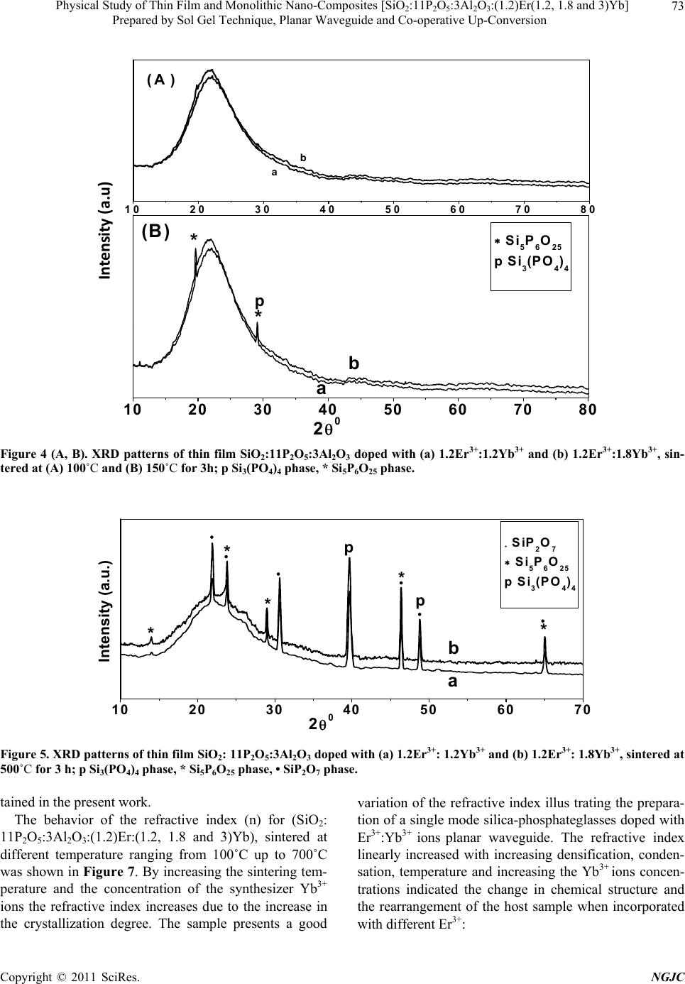 Physical Study of Thin Film and Monolithic Nano-Composites [SiO:11P O:3Al O:(1.2)Er(1.2, 1.8 and 3)Yb] 73 22 523 Prepared by Sol Gel Technique, Planar Waveguide and Co-operative Up-Conversion 10 20 30 40 50 6070 80 (A ) b a 10 2030 405060 7080 Si5P6O25 p Si3(PO4)4 b a (B) 2 0 * p * Intensity(a.u) Figure 4 (A, B). XRD patterns of thin film SiO2:11P2O5:3Al2O3 doped with (a) 1.2Er3+:1.2Yb3+ and (b) 1.2Er3+:1.8Yb3+, sin- tered at (A) 100˚C and (B) 150˚C for 3h; p Si3(PO4)4 phase, * Si5P6O25 phase. 10 20 30 40 50 60 70 a b Intensity (a.u.) 20 p * * * * SiP2O7 Si5P6O25 p Si3(PO4)4 * p Figure 5. XRD patterns of thin film SiO2: 11P2O5:3Al2O3 doped with (a) 1.2Er3+: 1.2Yb3+ and (b) 1.2Er3+: 1.8Yb3+, sintered at 500˚C for 3 h; p Si3(PO4)4 phase, * Si5P6O25 phase, • SiP2O7 phase. tained in the present work. The behavior of the refractive index (n) for (SiO2: 11P2O5:3Al2O3:(1.2)Er:(1.2, 1.8 and 3)Yb), sintered at different temperature ranging from 100˚C up to 700˚C was shown in Figure 7. By increasing the sintering tem- perature and the concentration of the synthesizer Yb3+ ions the refractive index increases due to the increase in the crystallization degree. The sample presents a good variation of the refractive index illus trating the prepara- tion of a single mode silica-phosphateglasses doped with Er3+:Yb3+ ions planar waveguide. The refractive index linearly increased with increasing densification, conden- sation, temperature and increasing the Yb3+ ions concen- trations indicated the change in chemical structure and the rearrangement of the host sample when incorporated ith different Er3+: w C opyright © 2011 SciRes. NGJC 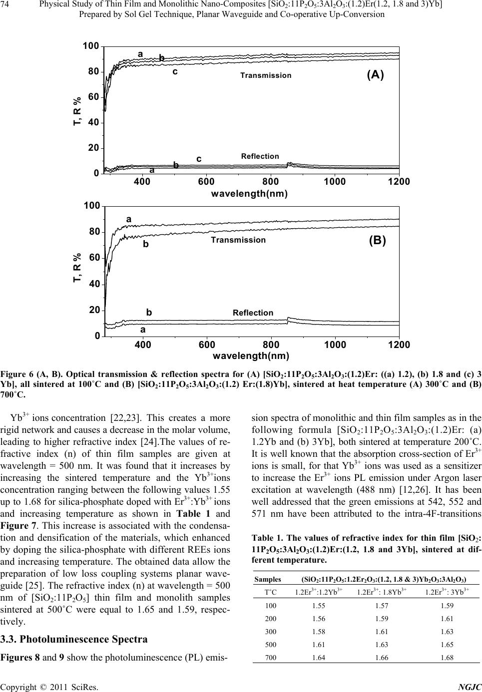 Physical Study of Thin Film and Monolithic Nano-Composites [SiO:11P O:3Al O:(1.2)Er(1.2, 1.8 and 3)Yb] 74 22 523 Prepared by Sol Gel Technique, Planar Waveguide and Co-operative Up-Conversion 4006008001000 1200 0 20 40 60 80 100 (B) T, R % w a velength(nm ) Transm ission Reflec tio n b b a a 4006008001000 1200 0 20 40 60 80 100 (A) T, R % wavelength(nm) Reflection Transmission c c b b a a Figure 6 (A, B). Optical transmission & reflection spectra for (A) [SiO2:11P2O5:3Al2O3:(1.2)Er: ((a) 1.2), (b) 1.8 and (c) 3 Yb], all sintered at 100˚C and (B) [SiO2:11P2O5:3Al2O3:(1.2) Er:(1.8)Yb], sintered at heat temperature (A) 300˚C and (B) 700˚C. Yb3+ ions concentration [22,23]. This creates a more rigid network and causes a decrease in the molar volume, leading to higher refractive index [24].The values of re- fractive index (n) of thin film samples are given at wavelength = 500 nm. It was found that it increases by increasing the sintered temperature and the Yb3+ions concentration ranging between the following values 1.55 up to 1.68 for silica-phosphate doped with Er3+:Yb3+ ions and increasing temperature as shown in Table 1 and Figure 7. This increase is associated with the condensa- tion and densification of the materials, which enhanced by doping the silica-phosphate with different REEs ions and increasing temperature. The obtained data allow the preparation of low loss coupling systems planar wave- guide [25]. The refractive index (n) at wavelength = 500 nm of [SiO2:11P2O5] thin film and monolith samples sintered at 500˚C were equal to 1.65 and 1.59, respec- tively. 3.3. Photoluminescence Spectra Figures 8 and 9 show the photoluminescence (PL) emis- sion spectra of monolithic and thin film samples as in the following formula [SiO2:11P2O5:3Al2O3:(1.2)Er: (a) 1.2Yb and (b) 3Yb], both sintered at temperature 200˚C. It is well known that the absorption cross-section of Er3+ ions is small, for that Yb3+ ions was used as a sensitizer to increase the Er3+ ions PL emission under Argon laser excitation at wavelength (488 nm) [12,26]. It has been well addressed that the green emissions at 542, 552 and 571 nm have been attributed to the intra-4F-transitions Table 1. The values of refractive index for thin film [SiO2: 11P2O5:3Al2O3:(1.2)Er:(1.2, 1.8 and 3Yb], sintered at dif- ferent temperature. Samples(SiO2:11P2O5:1.2Er2O3:(1.2, 1.8 & 3)Yb2O3:3Al2O3) T˚C 1.2Er3+:1.2Yb3+ 1.2Er3+: 1.8Yb3+ 1.2Er3+: 3Yb3+ 100 1.55 1.57 1.59 200 1.56 1.59 1.61 300 1.58 1.61 1.63 500 1.61 1.63 1.65 700 1.64 1.66 1.68 C opyright © 2011 SciRes. NGJC 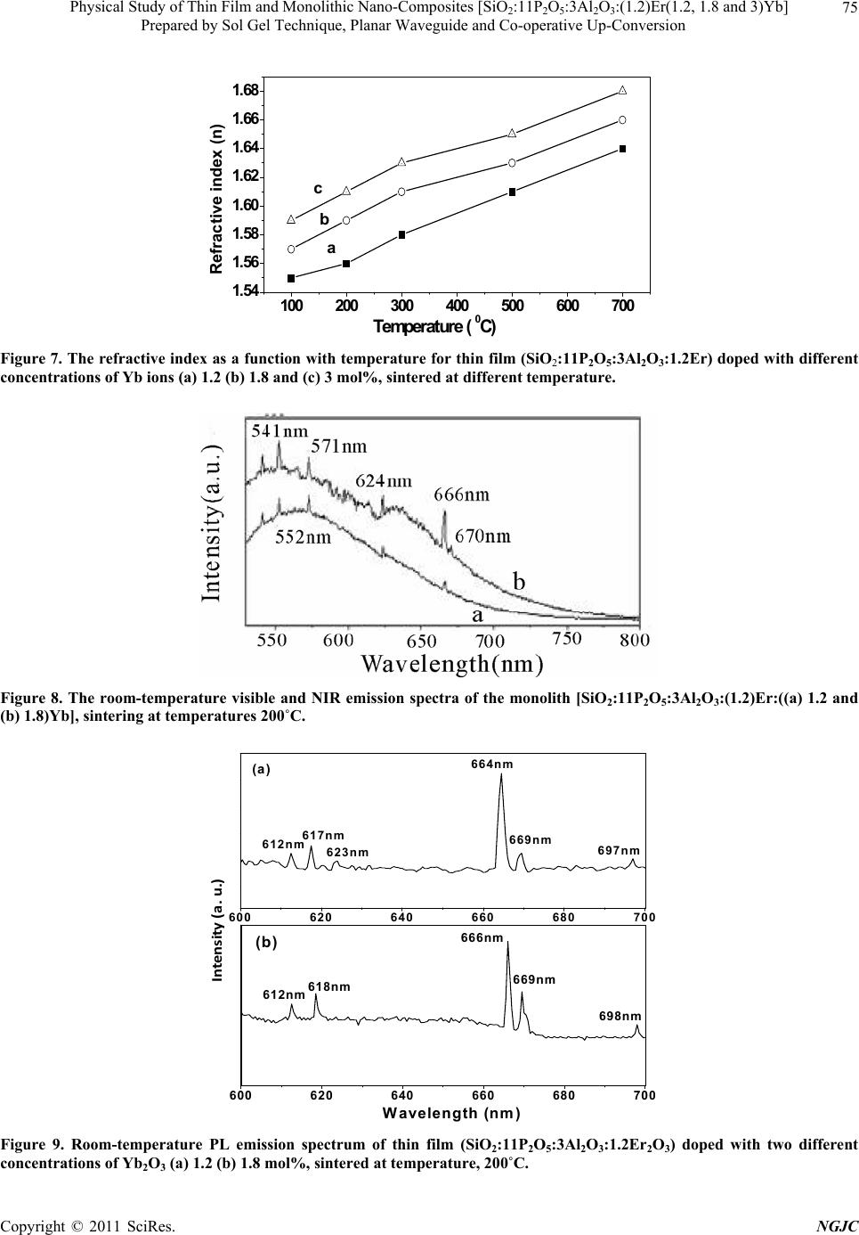 Physical Study of Thin Film and Monolithic Nano-Composites [SiO:11P O:3Al O:(1.2)Er(1.2, 1.8 and 3)Yb] 75 22 523 Prepared by Sol Gel Technique, Planar Waveguide and Co-operative Up-Conversion 100 200 300 400 500 600 700 1.54 1.56 1.58 1.60 1.62 1.64 1.66 1.68 Refractive ind ex (n) c b a Tem perature ( 0C) Figure 7. The refractive index as a function with temperature for thin film (SiO2:11P2O5:3Al2O3:1.2Er) doped with different concentrations of Yb ions (a) 1.2 (b) 1.8 and (c) 3 mol%, sintered at different temperature. Figure 8. The room-temperature visible and NIR emission spectra of the monolith [SiO2:11P2O5:3Al2O3:(1.2)Er:((a) 1.2 and (b) 1.8)Yb], sintering at temperatures 200˚C. 600620 640 660 680 700 (a) 697nm 669nm 664nm 623nm 617nm 612nm 600 620640 660 680 70 W avelength (nm ) (b) 698nm 669nm 666nm 618nm 612nm Intensity (a.u.) Figure 9. Room-temperature PL emission spectrum of thin film (SiO2:11P2O5:3Al2O3:1.2Er2O3) doped with two different oncentrations of Yb2O3 (a) 1.2 (b) 1.8 mol%, sintered at temperature, 200˚C. c C opyright © 2011 SciRes. NGJC 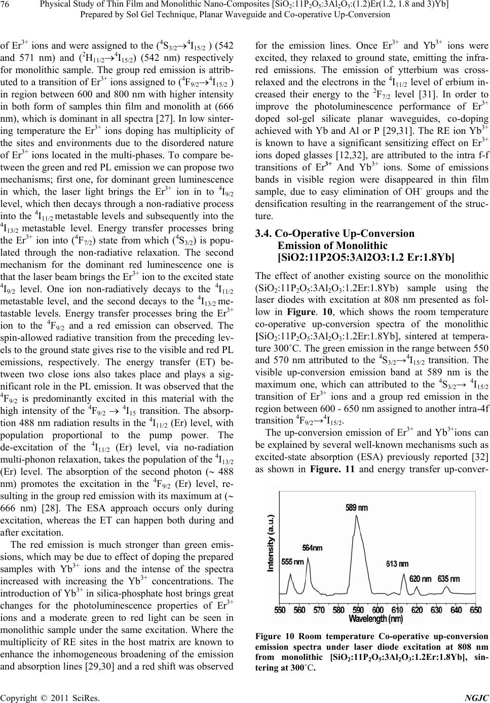 Physical Study of Thin Film and Monolithic Nano-Composites [SiO:11P O:3Al O:(1.2)Er(1.2, 1.8 and 3)Yb] 76 22 523 Prepared by Sol Gel Technique, Planar Waveguide and Co-operative Up-Conversion of Er3+ ions and were assigned to the (4S3/24I15/2 ) (542 and 571 nm) and (2H11/24I15/2) (542 nm) respectively for monolithic sample. The group red emission is attrib- uted to a transition of Er3+ ions assigned to (4F9/24I15/2 ) in region between 600 and 800 nm with higher intensity in both form of samples thin film and monolith at (666 nm), which is dominant in all spectra [27]. In low sinter- ing temperature the Er3+ ions doping has multiplicity of the sites and environments due to the disordered nature of Er3+ ions located in the multi-phases. To compare be- tween the green and red PL emission we can propose two mechanisms; first one, for dominant green luminescence in which, the laser light brings the Er3+ ion in to 4I9/2 level, which then decays through a non-radiative process into the 4I11/2 metastable levels and subsequently into the 4I13/2 metastable level. Energy transfer processes bring the Er3+ ion into (4F7/2) state from which (4S3/2) is popu- lated through the non-radiative relaxation. The second mechanism for the dominant red luminescence one is that the laser beam brings the Er3+ ion to the excited state 4I9/2 level. One ion non-radiatively decays to the 4I11/2 metastable level, and the second decays to the 4I13/2 me- tastable levels. Energy transfer processes bring the Er3+ ion to the 4F9/2 and a red emission can observed. The spin-allowed radiative transition from the preceding lev- els to the ground state gives rise to the visible and red PL emissions, respectively. The energy transfer (ET) be- tween two close ions also takes place and plays a sig- nificant role in the PL emission. It was observed that the 4F9/2 is predominantly excited in this material with the high intensity of the 4F9/2 4I15 transition. The absorp- tion 488 nm radiation results in the 4I11/2 (Er) level, with population proportional to the pump power. The de-excitation of the 4I11/2 (Er) level, via no-radiation multi-phonon relaxation, takes the population of the 4I13/2 (Er) level. The absorption of the second photon ( 488 nm) promotes the excitation in the 4F9/2 (Er) level, re- sulting in the group red emission with its maximum at ( 666 nm) [28]. The ESA approach occurs only during excitation, whereas the ET can happen both during and after excitation. The red emission is much stronger than green emis- sions, which may be due to effect of doping the prepared samples with Yb3+ ions and the intense of the spectra increased with increasing the Yb3+ concentrations. The introduction of Yb3+ in silica-phosphate host brings great changes for the photoluminescence properties of Er3+ ions and a moderate green to red light can be seen in monolithic sample under the same excitation. Where the multiplicity of RE sites in the host matrix are known to enhance the inhomogeneous broadening of the emission and absorption lines [29,30] and a red shift was observed for the emission lines. Once Er3+ and Yb3+ ions were excited, they relaxed to ground state, emitting the infra- red emissions. The emission of ytterbium was cross- relaxed and the electrons in the 4I11/2 level of erbium in- creased their energy to the 2F7/2 level [31]. In order to improve the photoluminescence performance of Er3+ doped sol-gel silicate planar waveguides, co-doping achieved with Yb and Al or P [29,31]. The RE ion Yb3+ is known to have a significant sensitizing effect on Er3+ ions doped glasses [12,32], are attributed to the intra f-f transitions of Er3+ And Yb3+ ions. Some of emissions bands in visible region were disappeared in thin film sample, due to easy elimination of OH- groups and the densification resulting in the rearrangement of the struc- ture. 3.4. Co-Operative Up-Conversion Emission of Monolithic [SiO2:11P2O5:3Al2O3:1.2 Er:1.8Yb] The effect of another existing source on the monolithic (SiO2:11P2O5:3Al2O3:1.2Er:1.8Yb) sample using the laser diodes with excitation at 808 nm presented as fol- low in Figure. 10, which shows the room temperature co-operative up-conversion spectra of the monolithic [SiO2:11P2O5:3Al2O3:1.2Er:1.8Yb], sintered at tempera- ture 300˚C. The green emission in the range between 550 and 570 nm attributed to the 4S3/2→4I15/2 transition. The visible up-conversion emission band at 589 nm is the maximum one, which can attributed to the 4S3/2→ 4I15/2 transition of Er3+ ions and a group red emission in the region between 600 - 650 nm assigned to another intra-4f transition 4F9/2→4I15/2. The up-conversion emission of Er3+ and Yb3+ions can be explained by several well-known mechanisms such as excited-state absorption (ESA) previously reported [32] as shown in Figure. 11 and energy transfer up-conver- Figure 10 Room temperature Co-operative up-conversion emission spectra under laser diode excitation at 808 nm from monolithic [SiO2:11P2O5:3Al2O3:1.2Er:1.8Yb], sin- tering at 300˚C. C opyright © 2011 SciRes. NGJC 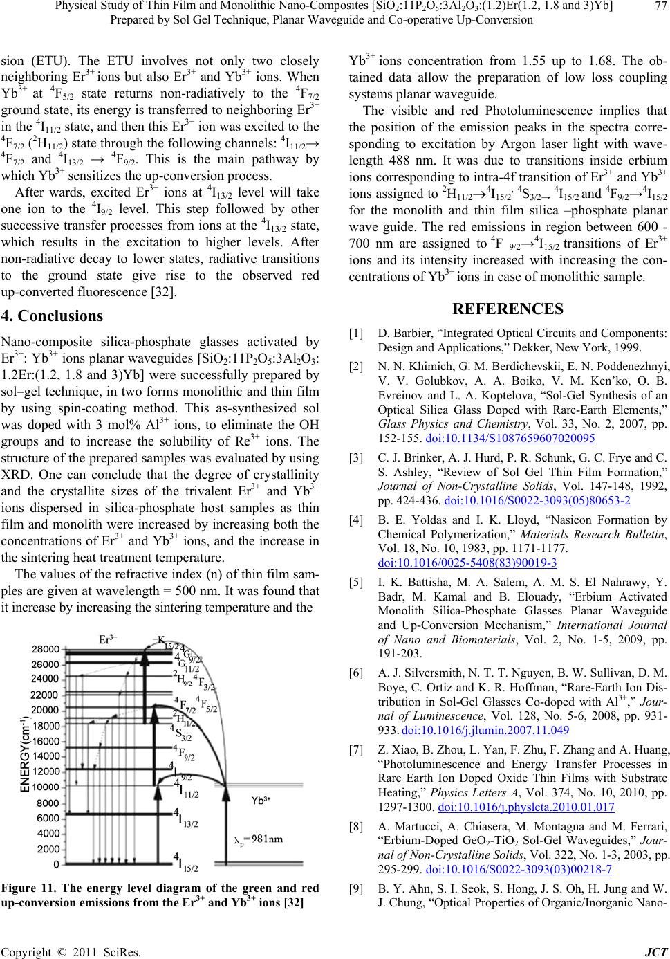 Physical Study of Thin Film and Monolithic Nano-Composites [SiO:11P O:3Al O:(1.2)Er(1.2, 1.8 and 3)Yb] 77 22 523 Prepared by Sol Gel Technique, Planar Waveguide and Co-operative Up-Conversion sion (ETU). The ETU involves not only two closely neighboring Er3+ ions but also Er3+ and Yb3+ ions. When Yb3+ at 4F5/2 state returns non-radiatively to the 4F7/2 ground state, its energy is transferred to neighboring Er3+ in the 4I11/2 state, and then this Er3+ ion was excited to the 4F7/2 (2H11/2) state through the following channels: 4I11/2→ 4F7/2 and 4I13/2 → 4F9/2. This is the main pathway by which Yb3+ sensitizes the up-conversion process. After wards, excited Er3+ ions at 4I13/2 level will take one ion to the 4I9/2 level. This step followed by other successive transfer processes from ions at the 4I13/2 state, which results in the excitation to higher levels. After non-radiative decay to lower states, radiative transitions to the ground state give rise to the observed red up-converted fluorescence [32]. 4. Conclusions Nano-composite silica-phosphate glasses activated by Er3+: Yb3+ ions planar waveguides [SiO2:11P2O5:3Al2O3: 1.2Er:(1.2, 1.8 and 3)Yb] were successfully prepared by sol–gel technique, in two forms monolithic and thin film by using spin-coating method. This as-synthesized sol was doped with 3 mol% Al3+ ions, to eliminate the OH groups and to increase the solubility of Re3+ ions. The structure of the prepared samples was evaluated by using XRD. One can conclude that the degree of crystallinity and the crystallite sizes of the trivalent Er3+ and Yb3+ ions dispersed in silica-phosphate host samples as thin film and monolith were increased by increasing both the concentrations of Er3+ and Yb3+ ions, and the increase in the sintering heat treatment temperature. The values of the refractive index (n) of thin film sam- ples are given at wavelength = 500 nm. It was found that it increase by increasing the sintering temperature and the Figure 11. The energy level diagram of the green and red up-conversion emissions from the Er3+ and Yb3+ ions [32] Yb3+ ions concentration from 1.55 up to 1.68. The ob- tained data allow the preparation of low loss coupling systems planar waveguide. The visible and red Photoluminescence implies that the position of the emission peaks in the spectra corre- sponding to excitation by Argon laser light with wave- length 488 nm. It was due to transitions inside erbium ions corresponding to intra-4f transition of Er3+ and Yb3+ ions assigned to 2H11/24I15/2, 4S3/2→ 4I15/2 and 4F9/2→4I15/2 for the monolith and thin film silica –phosphate planar wave guide. The red emissions in region between 600 - 700 nm are assigned to 4 F 9/2→4I15/2 transitions of Er3+ ions and its intensity increased with increasing the con- centrations of Yb3+ ions in case of monolithic sample. REFERENCES [1] D. Barbier, “Integrated Optical Circuits and Components: Design and Applications,” Dekker, New York, 1999. [2] N. N. Khimich, G. M. Berdichevskii, E. N. Poddenezhnyi, V. V. Golubkov, A. A. Boiko, V. M. Ken’ko, O. B. Evreinov and L. A. Koptelova, “Sol-Gel Synthesis of an Optical Silica Glass Doped with Rare-Earth Elements,” Glass Physics and Chemistry, Vol. 33, No. 2, 2007, pp. 152-155. doi:10.1134/S1087659607020095 [3] C. J. Brinker, A. J. Hurd, P. R. Schunk, G. C. Frye and C. S. Ashley, “Review of Sol Gel Thin Film Formation,” Journal of Non-Crystalline Solids, Vol. 147-148, 1992, pp. 424-436. doi:10.1016/S0022-3093(05)80653-2 [4] B. E. Yoldas and I. K. Lloyd, “Nasicon Formation by Chemical Polymerization,” Materials Research Bulletin, Vol. 18, No. 10, 1983, pp. 1171-1177. doi:10.1016/0025-5408(83)90019-3 [5] I. K. Battisha, M. A. Salem, A. M. S. El Nahrawy, Y. Badr, M. Kamal and B. Elouady, “Erbium Activated Monolith Silica-Phosphate Glasses Planar Waveguide and Up-Conversion Mechanism,” International Journal of Nano and Biomaterials, Vol. 2, No. 1-5, 2009, pp. 191-203. [6] A. J. Silversmith, N. T. T. Nguyen, B. W. Sullivan, D. M. Boye, C. Ortiz and K. R. Hoffman, “Rare-Earth Ion Dis- tribution in Sol-Gel Glasses Co-doped with Al3+,” Jour- nal of Luminescence, Vol. 128, No. 5-6, 2008, pp. 931- 933. doi:10.1016/j.jlumin.2007.11.049 [7] Z. Xiao, B. Zhou, L. Yan, F. Zhu, F. Zhang and A. Huang, “Photoluminescence and Energy Transfer Processes in Rare Earth Ion Doped Oxide Thin Films with Substrate Heating,” Physics Letters A, Vol. 374, No. 10, 2010, pp. 1297-1300. doi:10.1016/j.physleta.2010.01.017 [8] A. Martucci, A. Chiasera, M. Montagna and M. Ferrari, “Erbium-Doped GeO2-TiO2 Sol-Gel Waveguides,” Jour- nal of Non-Crystalline Solids, Vol. 322, No. 1-3, 2003, pp. 295-299. doi:10.1016/S0022-3093(03)00218-7 [9] B. Y. Ahn, S. I. Seok, S. Hong, J. S. Oh, H. Jung and W. J. Chung, “Optical Properties of Organic/Inorganic Nano- C opyright © 2011 SciRes. JCT  Physical Study of Thin Film and Monolithic Nano-Composites [SiO2:11P2O5:3Al2O3:(1.2)Er(1.2, 1.8 and 3)Yb] Prepared by Sol Gel Technique, Planar Waveguide and Co-operative Up-Conversion Copyright © 2011 SciRes. NJGC 78 composite Sol-Gel Films Containing LaPO4: Er, Yb Nanocrystals,” Optical Materials, Vol. 28, No. 4, 2006, pp. 374-379. doi:10.1016/j.optmat.2005.02.003 [10] R. Almeida, X. Min du, D. Barbier and X. Orignc, “Er3+- Doped Multicomponent Silicate Glass Planar Wave- guides Prepared by Sol-Gel Processing,” Journal of Sol- Gel Science and Technology, Vol. 14, No. 2, 1999, pp. 209-216. doi:10.1023/A:1008794202103 [11] M. J. F. Digonnet, “Rare-Earth-Doped Fiber Lasers and Amplifiers,” 2nd Edition, Dekker, New York, 2001. doi:10.1201/9780203904657 [12] M. J. F. Digonnet and E. Snitzer, “In Rare Earth Doped Fiber Lasers and Amplifiers,” In: M. J. F. Digonnet, Ed., Marcel Dekker, New York, 1993, Chapter 5. [13] Ph. Massiot, M. A. Centeno, I. Carrizosa and J. A. Odrio- zola, “Thermal Evaluation of Sol-Gel-Obtained Phospho- silicate Solids (Sipo),” Journal of Non-Crystalline Solids, Vol. 292, 2001, pp. 158-166. doi:10.1016/S0022-3093(01)00854-7 [14] T. L. Weeding, B. H. W. S. de Jong, W. S. Veeman and B. G. Aitken, “Silicon Coordination Changes from 4-Fold to 6-Fold on Devitrification of Silicon Phosphate Glass,” Nature, Vol. 318, 1982, pp. 351-352. doi:10.1038/318352a0 [15] Ph. Massiot, M. A Centeno, M. Gouriou, M. I. Domin- guez and J. A. Odriozola, “Sol-Gel Obtained Silicophos- phates as Materials to Retain Caesium at High Tempera- tures,” Journal of Materials Chemistry, Vol. 13, No. 1, 2003, pp. 67-74. doi:10.1039/b208698k [16] S. P. Szu, L. C. Klein and M. Greenblatt, “Effect of Pre- cursors on the Structure of Phosphosilicate Gels: 29Si and 31P MAS-NMR Study,” Journal of Non-Crystalline Sol- ids, Vol. 143, 1992, pp. 21-30. doi:10.1016/S0022-3093(05)80548-4 [17] D. Qiu, P. Guerry, J. C. Knowles, M. E. Smith and R. J. Newport, “Formation of Functional Phosphosilicate Gels from Phytic Acid and Tetraethyl Orthosilicate,” Journal of Sol-Gel Science and Technology, Vol. 48, No. 3, 2008, pp. 378-383. doi:10.1007/s10971-008-1818-9 [18] R. P. Rao and D. J. Devine, “RE-Activated Lanthanide Phosphate Phosphors for PDP Applications,” Journal of Luminescence, Vol. 87-89, 2000, pp. 1260-1263. doi:10.1016/S0022-2313(99)00551-7 [19] J. Dhanaraj, M. Geethalakshmi, R. Jagannathan and T. R. N. Kutty, “Eu3+-Doped Yttrium Oxysulfide Nanocrys- tals—Crystallite Size and Luminescence Transition(s),” Journal of Chemical Physics Letters, Vol. 387, No. 1-3, 2004, pp. 23-28. doi:10.1016/j.cplett.2004.01.079 [20] J. A. Sampaio, M. L. Baesso, S. Gama, A. A. Coelho, J. A. Eiras and I. A. Santos, “Rare Earth Doping Effect on the Elastic Moduli of Low Calcium Aluminosilicate Glasses,” Journal of Non-Crystalline Solids, Vol. 304, No. 1-4, 2002, pp. 293-298. doi:10.1016/S0022-3093(02)01037-2 [21] M. T. Wang and J. S. Cheng, “Viscosity and Thermal Expansion of Rare Earth Containing Soda-Lime-Silicate Glass,” Journal of Alloys and Compounds, Vol. 504, No. 1, 2010, pp. 273-276. doi:10.1016/j.jallcom.2010.08.134 [22] N. Kitamura, K. Fukumi, J. Nishii and N. Ohno, “Rela- tionship between Refractive Index and Density of Syn- thetic Silica Glasses,” Journal of Non-Crystalline Solids, Vol. 101, No. 12, 2009, pp. 123533-123540. [23] S. Shen, W. H. Chow, D. P. Steenson and A. Jha, “Fabri- cation of Er3+-Doped Oxyfluoride-Silicate Glass Film by Pulsed Laser Deposition for Planar Amplifier,” Journal of Non-Crystalline Solids, Vol. 355, No. 37-42, 2009, pp. 1893-1896. [24] E. T. Y. Lee and E. R. M. Taylor, “Compositional Effects on the Optical and Thermal Properties of Potassium Aluminophosphate Glasses,” Optical Materials, Vol. 27, No. 2, 2004, pp. 323-330. doi:10.1016/j.optmat.2004.02.029 [25] S. N. Houde-Walter, P. M. Peters, J. F. Stebbins and Q. Zeng, “Hydroxyl-Contents and Hydroxyl-Related Con- centration Quenching in Erbium Doped Aluminophosphate, Aluminosilicate and Fluorosilicate Glasses,” Journal of Non-Crystalline Solids, Vol. 286, No. 1-2, 2001, pp. 118-131. doi:10.1016/S0022-3093(00)00445-2 [26] P. Yang, M. K. Lu, C. F. Song, D. Xu, D. R. Yuan and F. Gu, “Photoluminescence Properties of Alkaline Metallic Ions Doped Sol-Gel Silica Glasses,” Materials Scie nce & Engineering, Vol. B90, No. 1-2, 2002, pp. 99-102. doi:10.1016/S0921-5107(01)00929-1 [27] V. Y. Timoshenko, D. M. Zhigunov, P. K. Kashkarov, O. A. Shalygina, S. A. Teterukov, R. J. Zhang, M. Zacharias, M. Fujii and Sh. Hayashi, “Photoluminescence Properties of Erbium-Doped Structures of Silicon Nanocrystals in Silicon Dioxide Matrix,” Journal of Non- Crystalline Solids, Vol. 352, No. 9-20, 2006, pp. 1192- 1195. [28] V. V. Filippov, P. P. Pershukevich, V. V. Kuznetsova and V. S. Homenko, “Photoluminescence Excitation Proper- ties of Porous Silicon with and without Er3+-Yb3+-Con- taining Complex,” Journal of Luminescence, Vol. 99, No. 3, 2002, pp. 185-195. [29] C. Li, B. Dong, S. Li and C. Song, “Er3+-Yb3+ Co-Doped Silicate Glass for Optical Temperature Sensor,” Chemical Physics Letters, Vol. 443, No. 4-6, 2007, pp. 426-429. [30] R. M. Almeida, A. C. Marques and S. Portal, “Glassy and Nano-Crystalline Photonic Materials and Structures by Sol-Gel,” Optical Materials, Vol. 27, No. 11, 2005, pp. 1718-1725. [31] J. Z. Wang, Z. Q. Shi, Y. Shi, L. Pu, L. J. Pan, R. Zhang, Y. D. Zheng, Z. S. Tao and F. Lu, “Broad Excitation of Er Luminescence in Er-Doped HfO2 Films,” Applied Physics A, Vol. 94, No. 2, 2009, pp. 399-403. [32] B. Dong, C. R. Li and M. K. Lei, “Green and Red Up-Conversion Emissions of Er3+-Yb3+ Codoped Al2O3 Powders Prepared by the Nonaqueous Sol-Gel Method,” Journal of Luminescence, Vol. 126, No. 2, 2007, pp. 441-446.
|