Journal of Electromagnetic Analysis and Applications
Vol. 3 No. 8 (2011) , Article ID: 6558 , 4 pages DOI:10.4236/jemaa.2011.38053
Development of Compact Ultra-Wideband (UWB) Microstrip Bandpass Filter
![]()
Department of Electronics and Communication Engineering, Pondicherry Engineering College, Puducherry, India.
Email: thirumalaivasank@pec.edu, rnakeeran@pec.edu
Received June 7th, 2011; revised July 4th, 2011; accepted July 15th, 2011.
Keywords: Ultra-Wideband, Microstrip, Bandpass Filter, Multiple Mode Resonator, Group Delay
ABSTRACT
Miniaturized Ultra-Wideband (UWB) microstrip bandpass filter with wide passband is presented. The filter is developed based on modified multiple mode resonator, which is formed by transversely attaching three pairs of non-uniform and folded stubs with lowpass and highpass sections. Both sides of high-impedance section are linked with two feed lines via direct coupled lines, resulting UWB bandpass filter. The designed filter provides 7 GHz passband between 2.5 and 9.5 GHz with approximately, –0.5 dB insertion loss, –35 dB minimum return loss at 6.85 GHz, linear phase over the passband and 110% of fractional bandwidth at –3 dB. The computed group delay variation in the passband for the filter is 0.02 ns. The overall dimension of the filter is 10.7 mm (length) × 3 mm (width) × 1.6 mm (thickness).
1. Introduction
The Ultra-Wideband (UWB) wireless communication technology has received greater attention after the Federal Communications Commission (FCC) decision to permit the unlicensed operation band from 3.1 to 10.6 GHz in February 2002 [1]. UWB filter is one of the most effective sub-systems of receiver used in controlling the spectrum of radio frequency signals. Researchers have been working towards the development of UWB filters with different geometries and design methodologies for more than one decade [2-10].
UWB filters having percentage fractional bandwidth of 110%, low insertion loss over the operating band, good performance at low frequency and a flat group delay are the major difficulties faced by the researchers while designing them [2]. Nevertheless, UWB filters with improved performances through different methods and structures [3-8] are discussed in the literature. The proposed UWB filter based on modified Multiple Mode Resonator (MMR) being discussed in this paper yields the response exactly (S11 and S12) as that of [3], which is a bandpass filter using Conductor Backed Co-planar Waveguide (CBCPW) back to back transition structure. CBCPW technology has unwanted bulk modes due to its parallel-plate modes [4], which is the main drawback of this structure. Moreover, the back to back transition has a complex design and difficult to fabricate.
In this paper, the UWB bandpass filter with wide passband and small size is developed and compared with existing structures. The features of the developed filter are compact in size with 10.7 mm in length against 16.0 mm in [3] and 12.5 mm in [6], good passband (insertion loss is about –0.5 dB at 6.85 GHz in simulation) and –3 dB passband from 2.5 to 9.5 GHz. Thus the developed filter offers a wide out-of-band rejection bandwidth and good performance in terms of group delay. This is fabricated using FR4 substrate with dielectric constant of 4.4, loss tangent 0.0004 and thickness of 1.6 mm. It is characterized and optimally designed using electromagnetic (EM) simulator, IE3D, which is part of the Zeland software package.
The rest of the paper is organized as follows: In Section 2, geometry, design and analysis of the developed UWB bandpass filter are discussed. Results and discussion are presented in Section 3. Section 4 concludes the paper.
2. Geometry and Analysis of UWB Bandpass Filter
The geometry of the proposed UWB bandpass filter is depicted in Figure 1 and a snap shot of fabricated bandpass filter is shown in Figure 2. This filter consists of three pairs of transversely connected stub-loaded modified MMR in the center section with two identical direct
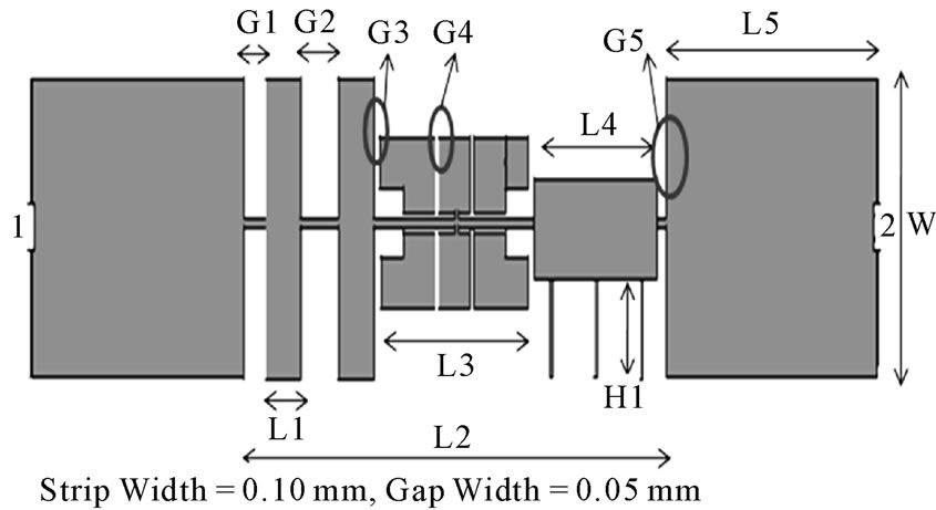
Figure 1. Proposed UWB bandpass filter geometry.
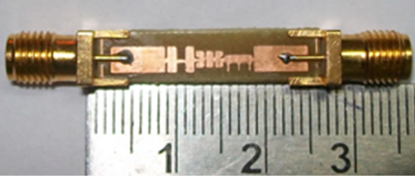
Figure 2. Snap shot of fabricated bandpass filter.
coupled lines in the left and right sections. Out of three transverse stubs, two of them are folded one. During design, the dimensions of folded stubs are properly trimmed to obtain its –3 dB higher frequency cut-off near 10 GHz. The middle section of the constituted MMR exhibits an excellent lowpass property and it is linked with external feed lines via direct coupled.
The presented UWB filter is the combination of a lowpass and a highpass filter using microstrip technology. The compact and low-loss nature of this filter is realized in microstrip line. The microstrip line filters are proved as versatile and low loss medium for filter design [8]. For the lowpass filter section, very high characteristic impedance is required. It is achieved with narrow stripline. For the highpass filter section, strong broadside coupling between wide line section and ground substrate is required to increase the inductance value, which results in small size and a wide passband filter response.
The physical parameters of the proposed bandpass fillter are optimized to the following values, G1 = 0.25 mm, G2 = 1 mm, G3 = 0.05 mm, G4 = 0.10 mm, G5 = 0.15 mm, L1 = 1 mm, L2 = 9.8 mm, L3 = 3.2 mm, L4 = 3.15 mm, L5 = 6 mm, H1 = 1 mm, and W = 3 mm to cover the entire UWB range of indoor mask. The minimum strip width and gap distance used in this structure are 0.10 mm and 0.05 mm respectively. The 3 mm long lowpass section (left side of the structure) consists of two open stubs and a distance gap. The length of the modified MMR with folded stubs is 3.20 mm and the length of the highpass filter section (right side of the structure) is 3.15 mm which comprises a uniform impedance resonator with three vertical limbs. To improve the resulting return loss while combining lowpass and highpass filters, a section of transmission line of 4.35 mm length is added between the two filter portions, resulting in an overall filter length of 10.7 mm.
3. Results and Discussions
The comparison of simulation and measured insertion and return losses of the developed bandpass filter is depicted in Figure 3. From the responses, it is clear that the filter provides ultra-wide passband from 3.1 to 10.6 GHz, very low and flat insertion loss of –0.5 dB and the minimum return loss of –35 dB. The measured in band insertion loss is about –1.5 dB at 6.85 GHz and return loss is about –37 dB at 9.4 GHz. The developed bandpass filter is more compact with comparable performances than filters available in the literature. Comparison of some of the filters with respect to their geometry, size and performance is tabulated in Table 1.
As shown in Figure 2, the two 50 ohm transmission lines are extended to accommodate the SMA connector to the scalar network analyzer for measurement. Using Hewlett Packard Network analyzer the insertion loss and return loss of the fabricated filter are measured. The measured results are well comparable to the simulated results. The small discrepancy between them might be due to fabrication tolerance.
The dimension of the entire filter structure comes around only 10.7 mm (length) × 3 mm (width). It is more compact in size with comparable performance than the filters available in the literature. To illustrate the dimension contraction achieved through the suggested filter in this paper, it is compared with filter discussed in [9] and understood that the developed filter consumes only 13% of the substrate of that filter which is equal to the size reduction of around 87%. It is also noticed that the filter has size reduction of 83% against the filter presented in [8] and, here, the proposed filter only takes 17% of its substrate area. In Figure 4, the simulation group delay for the filter is shown. Group delay variation in the passband of the filter is ±0.02 ns. Figure 5 shows the simulation phase of S21 for the filter. The response shows that the phase of S21 throughout the passband of developed filter is acceptably linear for UWB applications.
4. Conclusions
In this paper, miniaturized UWB bandpass filter with improved passband is designed, developed and characterized. The developed filter with passband of 7 GHz from 2.5 to 9.5 GHz has insertion loss of –0.5 dB and return loss of around –35 dB. The –3 dB percentage fractional bandwidth for the same is 110%. The computed
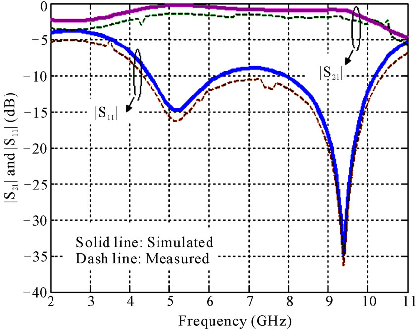
Figure 3. Comparison of simulation and measured insertion and return losses of the proposed and developed bandpass filter.
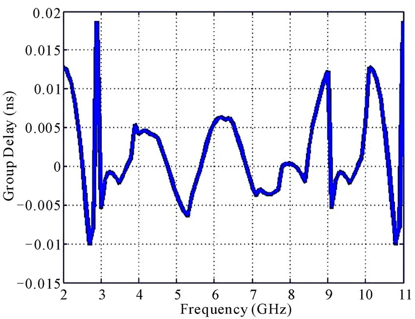
Figure 4. Simulation group delay of proposed bandpass filter.
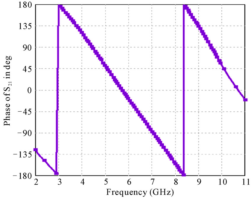
Figure 5. Simulation phase of the S21 of the proposed bandpass filter.
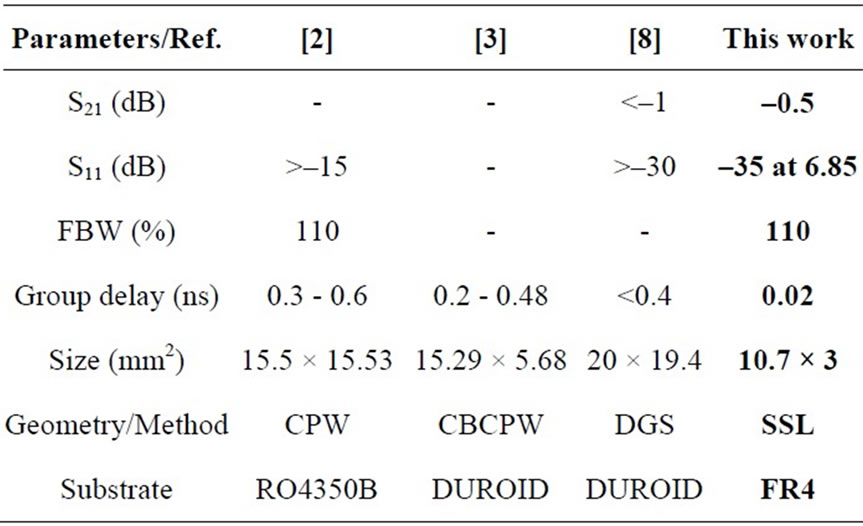
Table 1. Comparison of developed filter with best reported UWB bandpass filter in the literature.
group delay variation in the passband for the filter is 0.02 ns. The overall dimension of the filter is 10.7 mm (length) × 3 mm (width) × 1.6 mm (thickness). Thus the developed filter results in optimal performance in terms of scattering parameters, group delay and phase response to operate in the band of 3.1 - 10.6 GHz, which is suitable for UWB wireless systems.
REFERENCES
- Federal Communications Commission (FCC), “Revision of Part 15 of the Commission’s Rules Regarding Ultra-Wideband Transmission Systems FCC,” FCC Technical Report, ET-Docket FCC02-48, February 2002, pp. 98-153.
- S. N. Wang and N. W. Chen, “Compact Ultra-Wideband Coplanar Waveguide Bandpass Filter with Excellent Stopband Rejection,” Progress in Electromagnetics Research B, Vol. 17, 2009, pp. 15-28. doi:10.2528/PIERB09071008
- M. Nedil, T. A. Denidni and A. Djaiz, “Ultra-Wideband Microstrip to CB-CPW Transition Applied to Broadband Filter,” Electronics Letters, Vol. 43, No. 8, 2007, pp. 464-666. doi:10.1049/el:20070693
- W. H. Haydl, “On the Use of Vias in Conductor-Backed Coplanar Circuits,” IEEE Transactions on Microwave Theory and Techniques, Vol. 50, No. 6, 2002, pp. 1571- 1577. doi:10.1109/TMTT.2002.1006419
- W. J. Feng and W. Q. Che, “Novel Ultra-Wideband Bandpass Filter Using Shorted Coupled Lines and Transversal Transmission Line,” IEEE Microwave and Wireless Components Letters, Vol. 20, No. 10, 2010, pp. 548- 550. doi:10.1109/LMWC.2010.2055840
- S. Prabhu, J. Mandeep and S. Jovanovic, “Microstrip Bandpass Filter at S Band Using Capacitive Coupled Resonator,” Progress in Electromagnetics Research, PIER, Vol. 76, 2007, pp. 223-228. doi:10.2528/PIER07071205
- Z.-C. Hao and J.-S. Hong, “UWB Bandpass Filter Using Cascaded Miniature High-Pass and Low-Pass Filters with Multilayer Liquid Crystal Polymer Technology,” IEEE Transactions on Microwave Theory and Techniques, Vol. 58, No. 4, 2010, pp. 941-948. doi:10.1109/TMTT.2010.2042632
- J.-K. Lee and Y. S. Kim, “Ultra-Wideband Bandpass Filter with Improved Upper Stopband Performance Using Defect Ground Structure,” IEEE Microwave and Wireless Components Letters, Vol. 20, No. 6, 2010, pp. 316-318. doi:10.1109/LMWC.2010.2047469
- J.-S. Hong and H. Shaman, “An Optimum Ultra-Wideband Microstrip Filter,” Microwave and Optical Technology Letters, Vol. 47, No. 3, 2005, pp. 230-233. doi:10.1002/mop.21133
- Y. Yamamota, K. Li and O. Hashmoto, “Ultra-Wideband (UWB) Bandpass Filter Using Shunt Stub with Lumped Capacitor,” IEICE Electronics Express, Vol. 4, No. 7, 2007, pp. 222-231.