Materials Sciences and Applications
Vol.3 No.1(2012), Article ID:16970,6 pages DOI:10.4236/msa.2012.31006
Optical Properties of Polycrystalline Zinc Selenide Thin Films
![]()
1Department of Physics, S. S. V. P. S., ACS College Shindkheda, Dhule, India; 2Department of Physics, Z. B. Patil College, Dhule, India.
Email: *upkhairnar@rediffmail.com
Received June 3rd, 2011; revised August 5th, 2011; accepted December 28th, 2011
Keywords: Optical Materials; Vapour Deposition; X-Ray Diffraction; Band Gap
ABSTRACT
Thin films of ZnSe have been deposited onto glass substrates at 373 K by thermal evaporation technique. The X-ray diffractogram confirmed that ZnSe has cubic type crystal structure. The lattice parameters of thin films are almost matching with the JCPDS 5 - 552 data for Zinc Selenide. The transmittance and reflectance have been measured at normal and near normal incidence, respectively, in the spectral range 200 - 2500 nm. The dependence of absorption coefficient, α in the photon energy have been determined. Analysis of the result showed that films of different thicknesses, direct transition occurs with band gap energies ranges from 2.2 to 2.6 eV. Refractive indices and extinction coefficients have been evaluated in the above spectral range.
1. Introduction
ZnSe is an important semiconductor material with a large band gap (2.7 eV), which has a vast potential use in thin film devices and as n-type windows layer for thin film heterojunction solar cells [1-5]. These films can be prepared by a variety of techniques like vacuum evaporation [6], sputtering, pyrolysis and chemical deposition techniques. [7,8]. The recent developments on the fabrication of the II-VI blue light emitting diodes or blue laser diodes demand high quality ZnSe single crystal as a substrate for homoepitaxial growth. Similarly it is known that ZnSe differs from the other II-VI systems in symmetry. For example, when ZnSe is doped with phosphorous, C3v symmetry is reported both by experiment and theory [9]. II-VI semiconductor super lattices, excitonic properties are expected to play a prominent role in optical transitions due to the much larger exciton binding energies than these in III-V compound semiconductors [10]. An attractive idea from the technological point of view is a polycrystalline thin films deposition technique giving samples with good electro-optical properties. In the present paper the ZnSe thin films are analyzed for their structural and optical properties.
2. Experimental Details
The sets of various thicknesses of ZnSe thin films were deposited by sublimation of the compound in vacuum about 10–5 torr. The material used was in powder form. This was of “Aldrich Chemical Co.” make having purity of 99.99%. The glass slides having dimensions 75 mm × 25 mm × 1 mm were used as substrates. The glass slides were cleaned with warm dilute chromic acid, detergent solution, distilled water and isopropyl alcohol in that order. The samples of different thicknesses (500 Å, 1000 Å, 2000 Å, 3000 Å, 4000 Å, 5000 Å) were deposited under almost same environment. The thickness monitor model no. DTM - 101 provided by Hind-High Vac. The deposition rate was maintained (10 - 15 Å/sec) constant throughout the sample preparations. The source to substrate distance was kept constant (10 cm) and substrates were kept at constant temperature (373 K). Deposited samples were kept under vacuum overnight for each set.
Characterization of the Films
The structural characteristics of samples have been studied by X-ray diffractograms (Rigaku, Miniflex Japan) with CuKα radiation (1.5418 Å). The optical studies were carried out in the wavelength range of 200 - 2500 nm. A double beam spectrophotometer, Hitachi-330 Japan, was used for this purpose. The absorption coefficient, type of transition, optical constants and optical band gap were determined from these studies for all the evaporated thin films.
3. Results and Discussion
The X-ray diffractogram of the films indicates that films are polycrystalline in nature having cubic structure [11].
The reflectance and transmittance spectra of these samples were recorded using Hitachi spectrophotometer model-330 in the spectral region 200 - 2500 nm. Using these data, the absorption coefficient “α” has been calculated by applying the relation,
 (1)
(1)
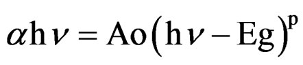
The absorption coefficient can be written in general form as a function of incident photon energy hν as using by Pankove [12],
 (2)
(2)
where, p has discrete values like ,
,  , 2 or more depending on whether the transition is direct or indirect and allowed or forbidden. In the direct and allowed cases
 where as for the direct but forbidden cases it is
 . But for the indirect and allowed case P = 2 and for the forbidden cases it will be 3 or more. Ao is a constant and given by

where  and mr are the effective and reduced masses of charges carriers respectively. Eg is the optical band gap, the value of “P” determined the nature of optical transition. The results have been analyzed according to the relation (2).
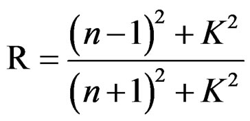
Optical constants, refractive indices and extinction coefficients, have been evaluated from the reflection data and using the relations by Goswami [13].
 (3)
(3)
and
 (4)
(4)
Absorption coefficients have been evaluated using percentage transmittance data as a function of wavelength presented in Figure 1 for the samples of different thicknesses. The plot of 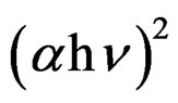 versus hν is presented in Figure 2 and Figure 3. These figures show clearly linear dependence for the value of
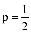 . This is attributed to an allowed and direct transition with direct band gap energies [14]. The evaluated band gap energies are 2.0, 2.2, 2.5, 2.6 and 2.6 eV for the samples of thicknesses 1000 Å, 2000 Å, 3000 Å, 4000 Å and 5000 Å respect-
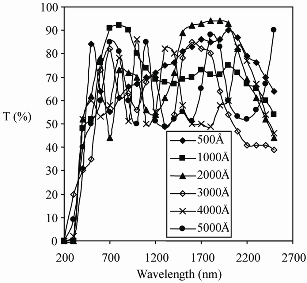
Figure 1. Spectral behavior of transmittance of ZnSe thin films of different thicknesses.

Figure 2. Variation of  with photon energy for thickness.
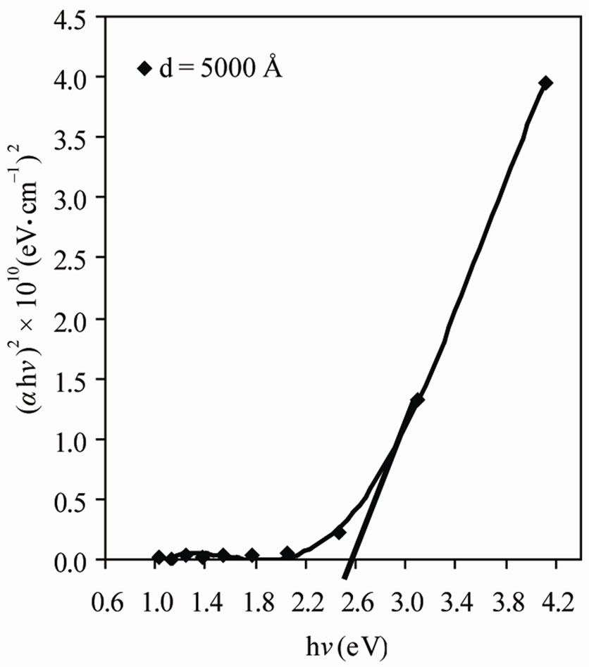
Figure 3. Variation of  with photon energy for thickness.
tively clearly indicating dependence on thicknesses of films.
It was attempted to plot  versus hν for the samples of different thicknesses. These plots did not show any linear dependence indicating that the transitions are direct.
The bulk ZnSe possesses an optical band gap of 2.58 eV. Estrada [15] was produced transparent ZnSe in most parts of the visible region. In present work the band gap value is higher than that of bulk material and also thickness dependence. This may be due to presence of quantum size effect [16,17]. This may be due to formation of very small crystalline size in the thin films. It is obvious that films of small thicknesses are more strained, have small size crystallites and weakly oriented which together lead to highly absorbing films.
The variation of refractive indices and extinction coefficients as a function of wavelength is represented in Figures 4-6 respectively for the thicknesses 3000 Å, 4000 Å, 5000 Å. From these figures it is found that variations in refractive indices and extinction coefficients are oscillatory in nature. It is observed that the number of maxima and minima depend upon the thickness of the film sample as mentioned by Khairnar [18]. This comparative study reveals the following facts:
1) For the thinnest sample of thickness 500 Å, there two maxima and one minima in the variation of “n”, while there is only one maxima and minima in the variation of “k”.
2) For the sample of thickness 1000 Å, there are two maxima and minima in the variation of “n” and “k” as a function of wavelength.
3) In the case of sample of thickness 2000 Å, there are three well defined maxima and minima in the variation of “n” and “k” as function of wavelength.
4) In the sample of thickness 3000 Å, there are four
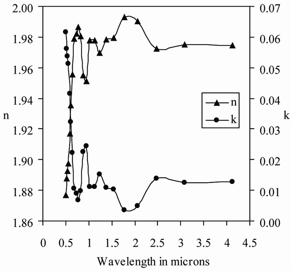
Figure 4. Variation of n and k wavelength (d = 3000 Å).
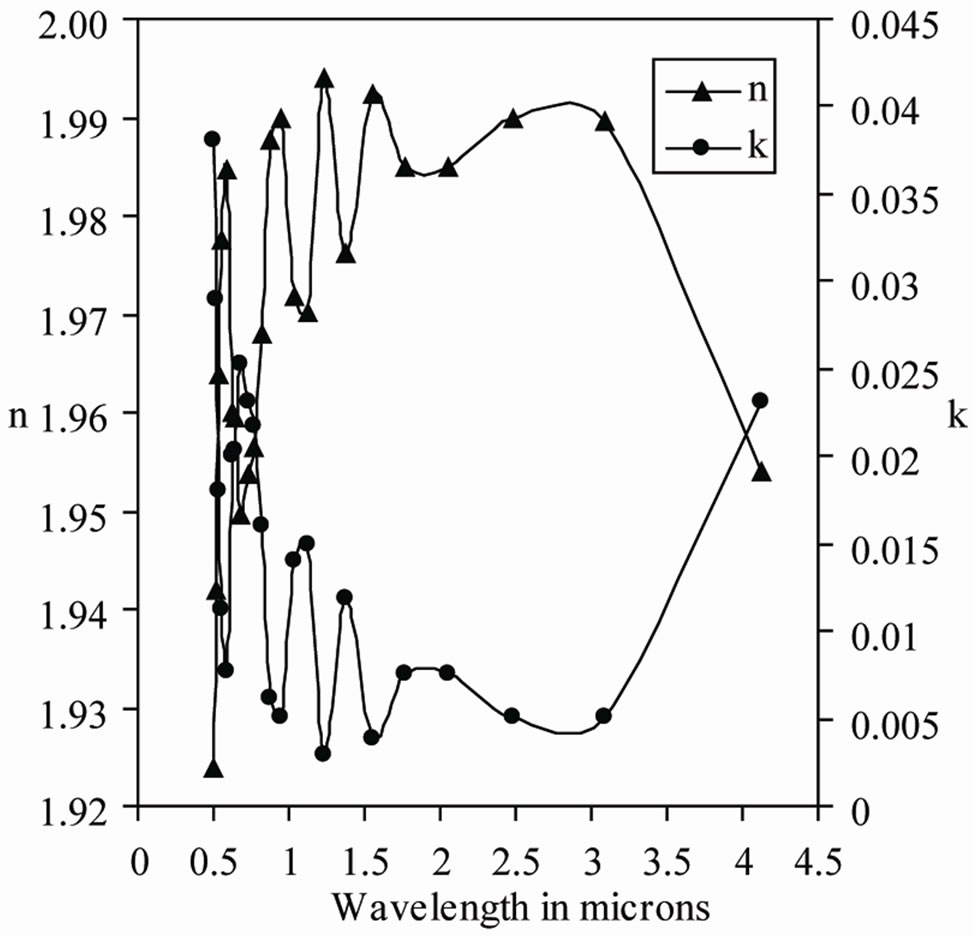
Figure 5. Variation of n and k wavelength (d = 4000 Å).
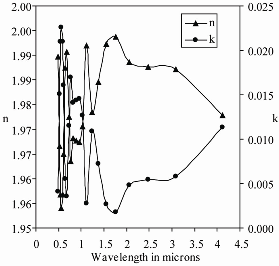
Figure 6. Variation of n and k wavelength (d = 5000 Å).
well defined maxima and minima in the variation of “n” and “k” as a function of wavelength.
5) For the sample of thickness 4000 Å, there are five well defined maxima and minima in the variation of “n” and “k” as a function of wavelength.
6) For the highest thickness of 5000 Å, there are six well defined maxima and minima in the variation of “n” and “k” as a function of wavelength.
Refractive index varies in the range from 1.75 to 2.05 while the range of extinction coefficient is from 0.002 to 0.18. This is represented in Table 1.
The XRD’s of ZnSe thin films of thicknesses 3000, 4000 and 5000 Å are shown in Figure 7 from these Xray diffractograms, it is observed that the peak intensity increases as the thickness of the sample increases. The peak intensity is observed at 2θ = 28.40 for almost all samples. This observed peak is identified as (111) plane of the standard data file JCPDS indicating cubic structure
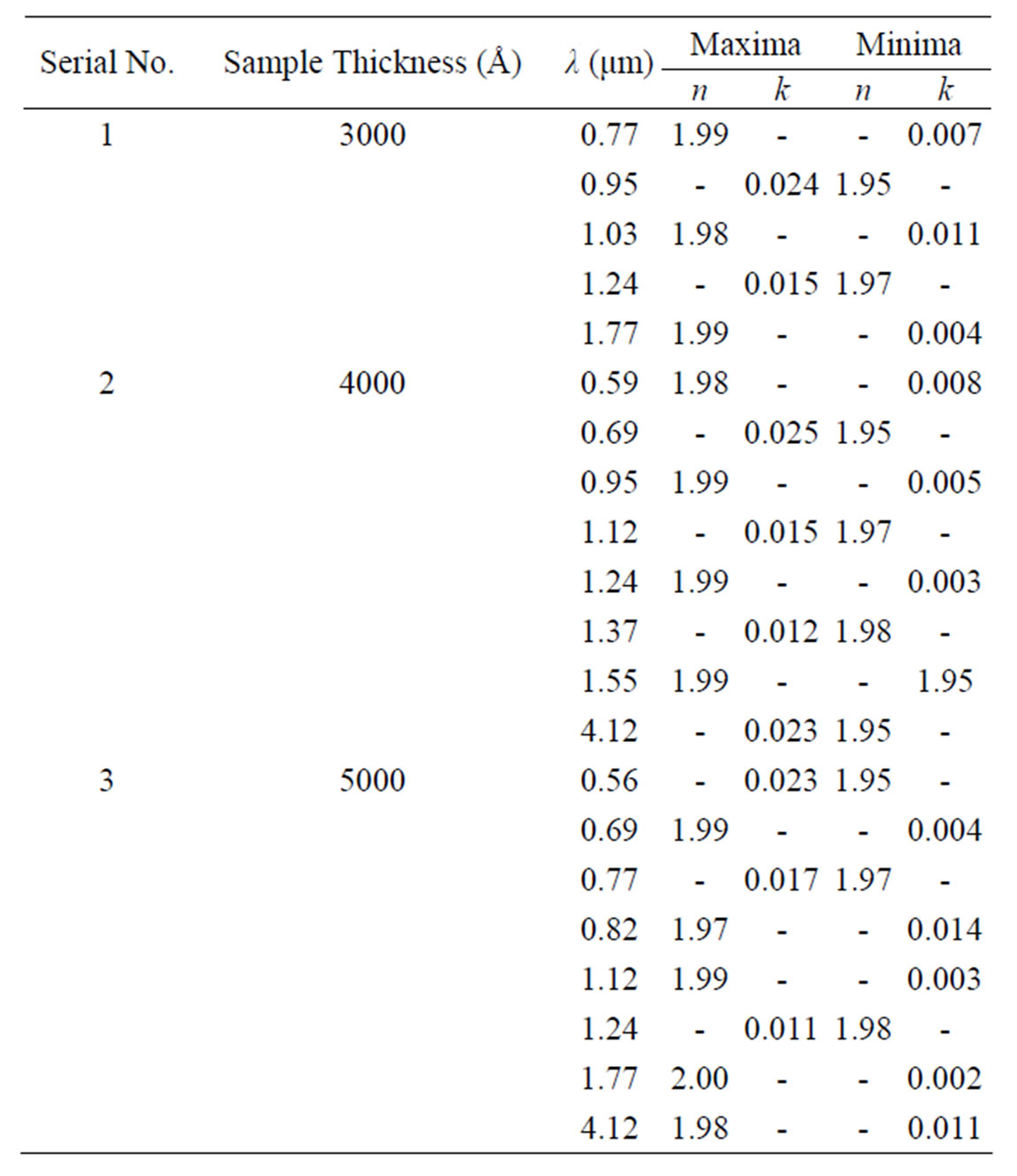
Table 1. Well-defined maxima and minima on variation of n and k.
having lattice parameter a = 5.4387Å.
The comparison of standard and observed data is presented in Table 2. This shows a preferred orientation in film growth along (111) plane [19,20]. The grain size of these films was estimated using Scherrer formula by ElKadry [21].

where K is a shape factor usually ,
, ![]() is the wavelength of the X-ray (1.5418 Å),
is the wavelength of the X-ray (1.5418 Å),  is the Bragg’s angle and “B” is the corrected FWHM. The estimated, values of grain size are very small of the order of 42.3 nm [22]. The estimated lattice parameter value from computer program POWD (an Interpretation and indexing Program, Version 2.2), a = 5.4387 is in good agreement with standard a = 5.667 (JCPDS 5 - 552).
4. Conclusion
Single-phase polycrystalline ZnSe films have been depo-
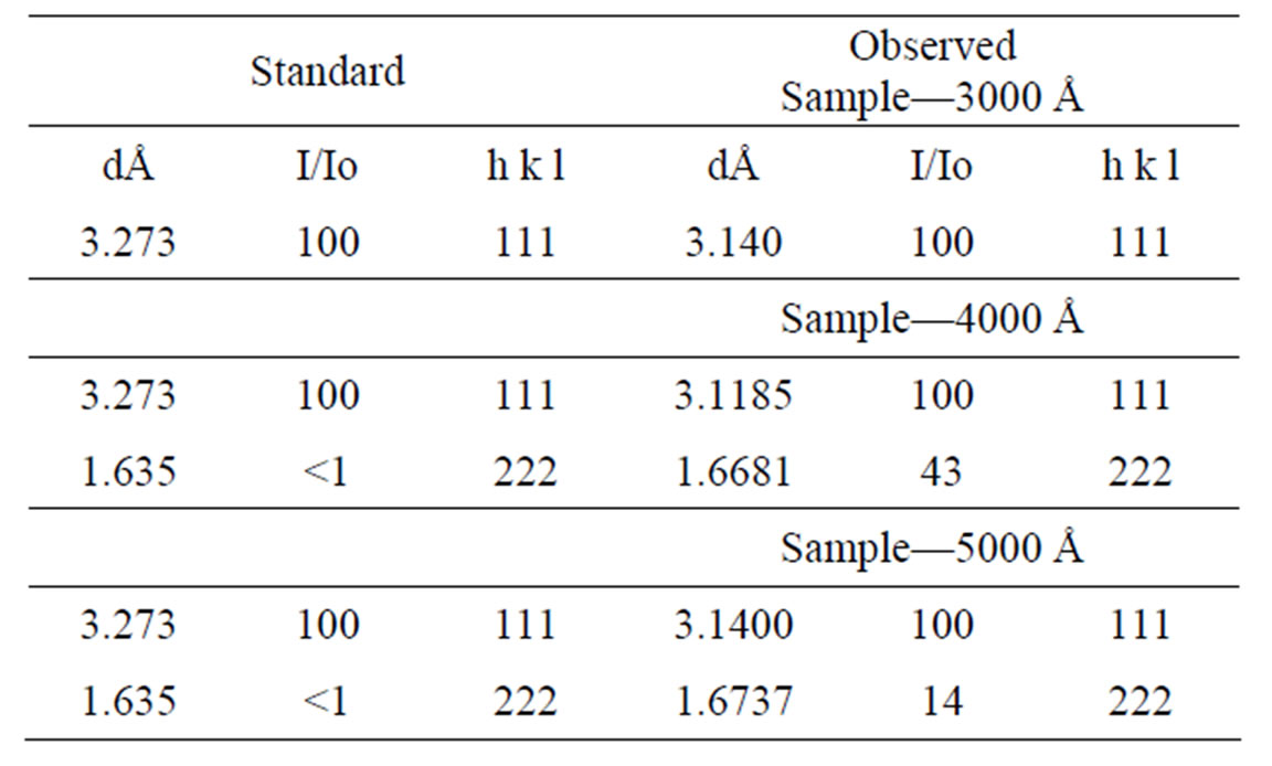
Table 2. Comparison of standard and observed XRD data.
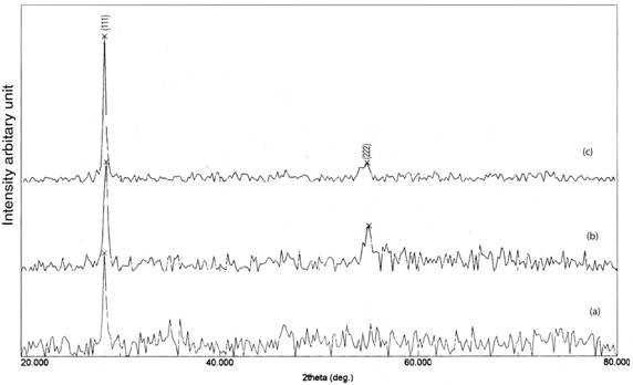
Figure 7. X-ray diffractogram of ZnSe thin films of different thicknesses. (a) 3000 Å; (b) 4000 Å; and (c) 5000 Å.
sited into amorphous glass substrates as revealed from XRD analysis and evaluated small grain size in the order of 42.3 nm. The dependence of the optical parameters of the films on the light energy supports the direct character of the interband transition through an optical band gap in the range 2.0 - 2.6 eV. The variation in optical constants as a function of wavelength is oscillatory in nature having well defined maxima and minima, which depends on the thickness of the sample.
5. Acknowledgements
The authors are thankful to Prof. Dr. M. V. Patil, Principle, S. S. V. P. S. ACS College, Shindkheda. The authors are also grateful to Prof. Dr. P. P. Patil, Head, Department of Physics, North Maharashtra University, Jalgaon.
REFERENCES
- B. B. Ismaiel and R. D. Gold, “Structural and Electrical Properties of Evaporated Thin Films of Cadmium Telluride,” Physica Status Solidi A, Vol. 115, No. 1, 1989, pp. 237-245. doi:10.1002/pssa.2211150126
- K. L. Chopra and S. R. Das, “Thin Film Solar Cells,” Plenum Press, New York, 1983.
- C. S. Yang, Y. P. Hsieh, M. C. Kuo, P. Y. Tseng, Z. W. Yeh, K. C. Chiu, J. L. Shen, A. H. M. Chu, W. C. Chou and W. H. Lan, “Compressive Strain Induced Heavy Hole and Light Hole Splitting of Zn1-xCdxSe Epilayers Grown by Molecular Beam Epitaxy,” Materials Chemistry and Physics, Vol. 78, No. 3, 2003, pp. 602-607. doi:10.1016/S0254-0584(01)00585-5
- B. Mokili, Y. Charreire, R. Cortes and D. Lincot, “Extended X-Ray Absorption Fine Structure Studies of Zinc Hydroxo-Sulphide Thin Films Chemically Deposited from Aqueous Solution,” Thin Solid Films, Vol. 288, No. 1-2, 1996, pp. 21-28. doi:10.1016/S0040-6090(96)08805-0
- L. N. Tripathi, S. K. Mistra and R. N. Singh, “Luminescence in ZnSe doped with Pr and (Sn, Pr) Phosphers,” Indian Journal of Pure and Applied Physics, Vol. 31, 1993, pp. 899-906.
- G. K. M. Thutupalli and S. G. Tomlin, “The Optical Properties of Thin Films of Cadmium and Zinc Selenides and Tellurides,” Journal of Physics D: Applied Physics, Vol. 9, No. 11, 1976, pp. 1639-1646. doi:10.1088/0022-3727/9/11/010
- R. Kuzel, Jr., V. Valvoda, M. Chladek, J. Musil and J. Matous, “XRD Microstructural Study of Zn Films Deposited by Unbalanced Magnetron Sputtering,” Thin Solid Films, Vol. 263, No. 2, 1995, pp. 150-158. doi:10.1016/0040-6090(95)06575-X
- K. L. Chopra R. C. Kainthla, D. K. Pandya and A. P. Thakoor, In: G. Hass et al., Eds., Physics of Thin Films, Academic Press, Inc., New York, 1982, p. 167.
- A. K. Balasubramanian, N. Sankar, S. K. Ramakrishnan and K. Ramachandran, “Thermal Conductivity of ZnSe by Molecular Dynamics Simulation,” Crystal Research and Technology, Vol. 39, No. 6, 2004, pp. 558-563. doi:10.1002/crat.200310224
- J. Bang, J. Park, J.-H. Lee, N. Won, J. Nam, J. Lim, B.-Y. Chang, H.-J. Lee, B. Chon, J. Shin, J.-B. Park, J.-H. Choi, K. Cho, S.-M. Park, T. Joo and S. Kim, “ZnTe/ZnSe (Core/Shell) Type-II Quantum Dots: Their Optical and Photovoltaic Properties,” Chemistry of Materials, Vol. 22, No. 1, 2010, pp. 233-240. doi:10.1021/cm9027995
- M. El Sherif, F. S. Terra and S. A. Khodier, “Optical Charateristers of Thin ZnSe Films of Different Thicknesses,” Journal of Materials Science: Materials in Electronics, Vol. 7, 1996, pp. 391-395.
- J. J. Pankove, “Optical Processes in Semiconductors,” Prentice Hall, Upper Saddle River, 1971.
- A. Goswami, “Thin Film Fundamentals,” New Age International Pvt. Ltd., New Delhi, 1996.
- Z. P. Guan, Z. H. Zheng, Y. M. Lu, B. J. Yang and X. W. Fan, “Dispersive Optical Bistability in ZnCdSe-ZnSe/ GaAs Strained-Layer Superlattices on Reflection at Room Temperature,” Thin Solid Films, Vol. 263, No. 2, 1995, pp. 203-205. doi:10.1016/0040-6090(95)06532-6
- C. A. Estrada, R. A. Zingaro, E. A. Meyers, P. K. Nair and M. T. S. Nair, “Modification of Chemically Deposited ZnSe Thin Films by Ion Exchange Reaction with Copper Ions in Solution,” Thin Solid Films, Vol. 247, No. 2, 1994, pp. 208-212. doi:10.1016/0040-6090(94)90801-X
- S. V. Svechnikov and E. B. Kaganovich, “CdSxSe1−x Photosensitive Films: Preparation, Properties and Use for Photodetectors in Optoelectronics,” Thin Solid Films, Vol. 66, No. 1, 1980, pp. 41-54. doi:10.1016/0040-6090(80)90071-1
- G. N. Chaudhari, S. Manorama and V. J. Rao, “Deposition of ZnS0.056Se0.944 Thin Films on GaAs(110) Substrates: A New Chemical Growth Technique,” Thin Solid Films, Vol. 208, No. 2, 1992, pp. 243-246. doi:10.1016/0040-6090(92)90650-Z
- U. P. Khairnar, D. S. Bhavsar, R. U. Vaidya and G. P. Bhavsar, “Optical Properties of Thermally Evaporated Cadmium Telluride Thin Films,” Materials Chemistry and Physics, Vol. 80, No. 2, 2003, pp. 421-427. doi:10.1016/S0254-0584(02)00336-X
- E. Khawaja and S. G. Tomlin, “The Optical Constants of Thin Evaporated Films of Cadmium and Zinc Sulphides,” Journal of Physics D: Applied Physics, Vol. 8, No. 5, 1975, pp. 581-594. doi:10.1088/0022-3727/8/5/019
- S. Soundeswaran, O. S. Kumar, R. Dhanasekaran, P. Ramasamy, R. Kumaresen and M. Ichimura, “Growth of ZnSe Thin Films by Electrocrystallization Technique,” Materials Chemistry and Physics, Vol. 82, No. 2, 2003, pp. 268-272. doi:10.1016/S0254-0584(03)00226-8
- N. El-Kadry, A. Ashour and S. A. Mahmoud, “Structural Dependence of d.c. Electrical Properties of Physically Deposited CdTe Thin Films,” Thin Solid Films, Vol. 269, No. 1-2, 1995, pp. 112-116. doi:10.1016/0040-6090(95)06869-4
- Y. Fan, J. Han, L. He, J. Saraie and R. L. Gunshor, “Graded Band Gap Ohmic Contact to P-ZnSe,” Applied Physics Letters, Vol. 61, No. 26, 1992, pp. 3160-3162. doi:10.1063/1.107945