Circuits and Systems
Vol. 3 No. 2 (2012) , Article ID: 18539 , 5 pages DOI:10.4236/cs.2012.32021
A New Current-Controlled-Power Technique for Small Signal Applications
Department of Electronic Engineering, South-East Asia University, Bangkok, Thailand
Email: aone_mon@hotmail.com
Received November 24, 2011; revised December 26, 2011; accepted January 3, 2012
Keywords: Current-Controlled-Power; Full-Wave Rectifier; Analog Signal Processing
ABSTRACT
In this paper, a new current-controlled-power technique for small signal applications is presented. The proposed technique needs no passive devices (a resistor and a capacitor) but the well-known SCR technique needs, thus the proposed technique is very suitable for an IC process. An example application as a new current-controlled-power CMOS fullwave rectifier is also given. The example application is simulated by using the SPICE program. Simulation results show that the proposed technique can work well; the controlled-current from 0 µA to 5.5 µA produces the peak area amplitude from 100 mV to 0 mV to the load.
1. Introduction
As is well known, it is hard to find the device that operates as a silicon-controlled rectifier (SCR) [1] for controlling the power in small signal applications. In this paper, the author presents a new current-controlledtechnique for small signal applications. The proposed technique yields the advantages:
• The proposed technique needs no a capacitor and a resistor but the well-known SCR technique needs; therefore, without passive devices, the proposed technique uses a much smaller chip area in the IC process [2].
• The proposed technique works with a small signal but the SCR technique cannot work because of the threshold voltage of the SCR [1].
• The proposed technique can also work with a large signal by driving a power bipolar transistor.
• The proposed technique with current-controlled is very suitable for an automatic control system by the current feedback. Whereas the SCR technique uses the RC time constant for clipping time [1], it is hard for the automatic control system.
The example application as a new current-controlledpower CMOS full-wave rectifier is also presented. It provides the advantages as follows.
• The new full-wave rectifier works both full-wave rectification and current-controlled-power operation. But the previous proposed full-wave rectifiers cannot control the output power.
• The new rectifier uses all MOSs with typical structure thus it is very suitable for IC processes [3].
• The new rectifier, its core operates in balanced mode resulting in a low noise output [4].
• Using the new rectifier, one can independently control the positive part and the negative part of the input signal, this yields more precision control.
2. Proposed Current-Controlled-Power Technique
The proposed technique is shown in Figure 1(a) and its signals are shown in Figure 1(b). The operation is as follows. ICL1 is fed to shift down the input differential current signal (Iin+). It will decrease the amplitude and area of the positive signal and will increase those of the negative signal. The bias source (Vb) is the voltage or current, for turning-on the current mirror (MN1 and MN2) all the time for very small signal operation. The Vb must be the minimum voltage or current to make the minimum offset at the output (Iout). The Iout is the positive signal rectified by the current mirror. Because the input signal is shifted down, one must compensate this for (Iin–) by feeding ICL2 for balancing the input signal.
Note the proposed technique that the output is a horizontal clipped signal but the well-known SCR technique the output is a vertical clipped signal. The proposed technique with all active devices is better than the SCR technique with the resistor and capacitor devices in view of IC fabrication. Additionally, the proposed technique with current-controlled is very suitable for automatic control system by a current feedback. Whereas the SCR
 (a) (b)
Figure 1. Proposed technique: (a) circuit and (b) operation.
technique uses the RC time constant for clipping time, it is hard for automatic control system. Moreover, the proposed technique can be used in high power applications; it can drive the high current bipolar transistor.
3. Application Example as a New Current-Controlled-Power Full-Wave Rectifier
The circuit in Figure 2 operates as a full-wave rectifier where ICL+1 = ICL+2 = ICL–1 = ICL–2 = 0. Its operation is as follows. The constant current source IC is mirrored by MI1 and MI3 to the drain of M3 (ID3); and is mirrored by MI1, MI2, MI4 and MI5 to the drain of M1 (ID1). The W/L ratios of MI1 to MI5 are equal, making ID1 = ID3. Moreover, using matched MOS transistors M1 to M4 [5], the input voltage is thus followed to a MOS resistor (RA) [6], the resistance of which is given by
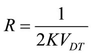 (1)
(1)
where MA1 and MA2 have the same characteristics; K = mCoxW/L, m is the carrier mobility, Cox is the gate capacitance per unit area, W and L are the channel width and length respectively; VDT = VDD – VT = –(VSS + VT), VDD = –VSS, VT is the threshold voltage.
Equation (1) is valid when both MA1 and MA2 maintain in the saturation region, which is true if
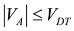 (2)
(2)
This input voltage creates the current Iin flowing through RA.
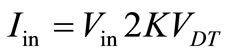 (3)
(3)
In Figure 2, Iin is mirrored by M5, M6, M9, and M10 as I1; and is mirrored by M5, M7, M9, and M11 as I4 = –I1. Furthermore, Iin is mirrored by M5, M8, M9, M12, M13, M14, M16, and M17 as I2; and is mirrored by M5, M8, M9, M12, M13, M15, M16, and M18 as I3. One assumes that the gain of all current mirrors is unity, thus
 (4)
(4)
When the input voltage is positive, the current mirror (M19 and M20) turns on and the current mirror (M21 and M22) turns off. Inversely, when the input voltage is negative, the current mirror (M19 and M20) turns off and the current mirror (M21 and M22) turns on, resulting in
 (5)
(5)
The drain currents of M20 and M22 are finally mirrored by M23 and M24 and then are converted to the voltage by RB. Using RA = RB by setting MA1 = MA2 = MB1 = MB2, the relation between input and output voltages (full-wave rectification) can be written as
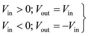 (6)
(6)
The bias sources (Vb1 and Vb2) in Figure 1 may be the voltage or current source. This bias source makes the MOSs in core 1 and core 2 (M19, M20, M21, and M22) turning-on all the time, to reduce the error at zero-crossing of the full-wave output signal.
Three main errors of the operation of the proposed rectifier can be considered. Assume that the error of W/L ratios of MOS transistors is ignored since it is very small in the present technology.
The first error is for transferring an input voltage to node A [5] because the currents ID1 and ID3 are slid resulting from the error of simple current mirrors (MI1 to MI5). This error can be minimized by using the better current mirrors (cascode or Wilson type); however, it requires higher supply voltage [7].
The second error is for mirroring the input current from RA to core 1 and core 2. And the last error is the error of core 1 and core 2. The second and the last errors can be reduced by using the better current mirrors as mentioned above.
The best way for setting three above errors to minimize, is compensation. The compensation can be done by adjusting the gain of core 1 and core 2 through the W/L ratios (of M20 for positive input and of M22 for negative input). In addition, adjusting the resistant of RB through W/L ratios of MB1 and MB2 is also compensation.
M2 and M4 must be in the saturation mode as M1 and M3; this yields the input operation range,
 (7)
(7)
where  [7], and α is the

Figure 2. Application example as a new current-controlled-power full-wave rectifier.
voltage gain between input and node A, ideally it must be unity.
In the same way, M6, M7, M8, M10, M11, M12, M14, M15, M17, and M18 have to be in the saturation mode. If these MOSs have the same parameters, one can write the operation range of signals at nodes B, C, D, and E as
 (8)
(8)
Using the same characteristics M5 to M18, considering Equations (2), (7), and (8), the operation range of the proposed full-wave rectifier is considered as (7).
Note that two signals of core 1 at nodes B and D, two signals are 180 degrees out-of-phase; hence, some inphase outside noise around the core will be cancelled, as well-known. It is also for core 2. This indicates that the proposed rectifier operates in a balanced mode, canceling some outside noise around the core.
As mentioned above, if we feed the control current (ICL+1 = ICL+2), we can control the peak area of the positive input signal (see Figure 1(b)). Moreover, by feeding ICL–1 = ICL–2, we also can control the peak area of the negative input signal. It is evident that we can independently control the positive part and the negative part of the input signal, this yields more precision control.
At this point, we can see that one application example of the new current-controlled-power technique is the new full-wave rectifier. The new rectifier can be realized by using all MOS transistors with typical structure. It is very suitable for the process of IC fabrication. Furthermore, not only full-wave rectification but also current-controlledpower operation, the proposed rectifier can work. The previous proposed rectifiers cannot operate this currentcontrolled-power function. Additionally, the balanced mode operation of the core gains a lower noise output.
4. Results
To verify the theoretical design, the application example as a new current-controlled-power full-wave rectifier was simulated by using parameters extracted from its layout (including parasitic capacitance) in a 0.5 μm AMI MOS transistor technology, through a level-49 model.
The supply voltage is ±1.2 V. For full-wave rectifier simulation, IC is 20 mA, Vb1 = Vb2 are the current sources of 5 μA, ICL+1 = ICL+2 = ICL–1 = ICL–2 are 0 μA. The W/L ratios of MA1 = MA2 = 1.5 μm/1.5 μm, MB1 = MB2 = 1.5 μm/3.9 μm, and other MOSs = 20 μm/0.6 μm, were chosen.
Figure 3 shows the output of the proposed full-wave rectifier with a sine wave input signal (100 mVpeak, 100 kHz). The amplitude error of the output signal is almost zero because of compensation by using RB > RA, by adjusting their W/L ratios as mentioned in Section 3. Also, the gain compensation can be done through the W/L ratios of M20, M22, and M24. The author tried to decrease the amplitude of the input signal; one found that the proposed rectifier can rectify a minimum voltage of 350 µVpeak. Changing frequency was done, the maximum operation frequency of the proposed rectifier was 30 MHz (–3 dB point).
For current-controlled-power operation, the author set ICL+1 = ICL+2 = ICL–1 = ICL–2 following to the left column of Table 1, the right column shows the rectified output peak area amplitude. According to the theory, it was (namely, more ICL+1 = ICL+2 = ICL–1 = ICL–2, more shifted-down signal, less output peak area amplitude).
As mentioned in Section 3 that we can independently control the positive part and the negative part of the input signal, this yields more precision control. We will show it here. The rectifier output can be divided to two parts for controlling (A. the positive input part and B. the negative input part shifted the phase by 180 degrees, by rectifier). A is controlled by ICL+1 = ICL+2 and B is controlled by ICL–1 = ICL–2. Figure 4 shows the full-wave rectified output with ICL+1 = ICL+2 = 1 μA and ICL–1 = ICL–2 = 3.5 μA (changing the frequency to 1 MHz). It also shows that we can independently control the positive part and the negative part of the input signal, giving more precision control. Moreover, the proposed current-controlledpower full-wave rectifier is very suitable for an automatic control system by the current feedback. Whereas the SCR technique uses the RC time constant for clipping time, it is hard for the automatic control system.
Absolutely, not only full-wave rectification but also current-controlled-power operation, the proposed rectifier can work. The previous proposed rectifiers cannot operate this current-controlled-power function.
5. Conclusions
In this paper, the author has reported a new current-controlled-power technique that can be useful in analog small signal processing. The proposed technique needs no passive devices; it is very suitable for the IC process. The proposed technique can also work with a large signal by driving a power bipolar transistor. The proposed technique is very suitable for an automatic control system by the current feedback.
An application example as a new current-controlledpower full-wave rectifier has also been proposed. The new full-wave rectifier works both full-wave rectification
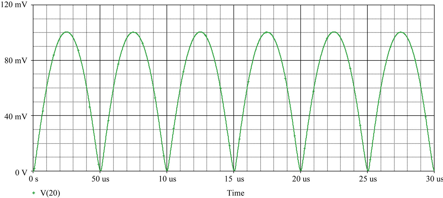
Figure 3. Output of the proposed current-controlled-power full-wave rectifier (ICL+1 = ICL+2 = ICL–1 = ICL–2 = 0) with an input sine wave of 100 mVpeak, 100 kHz.
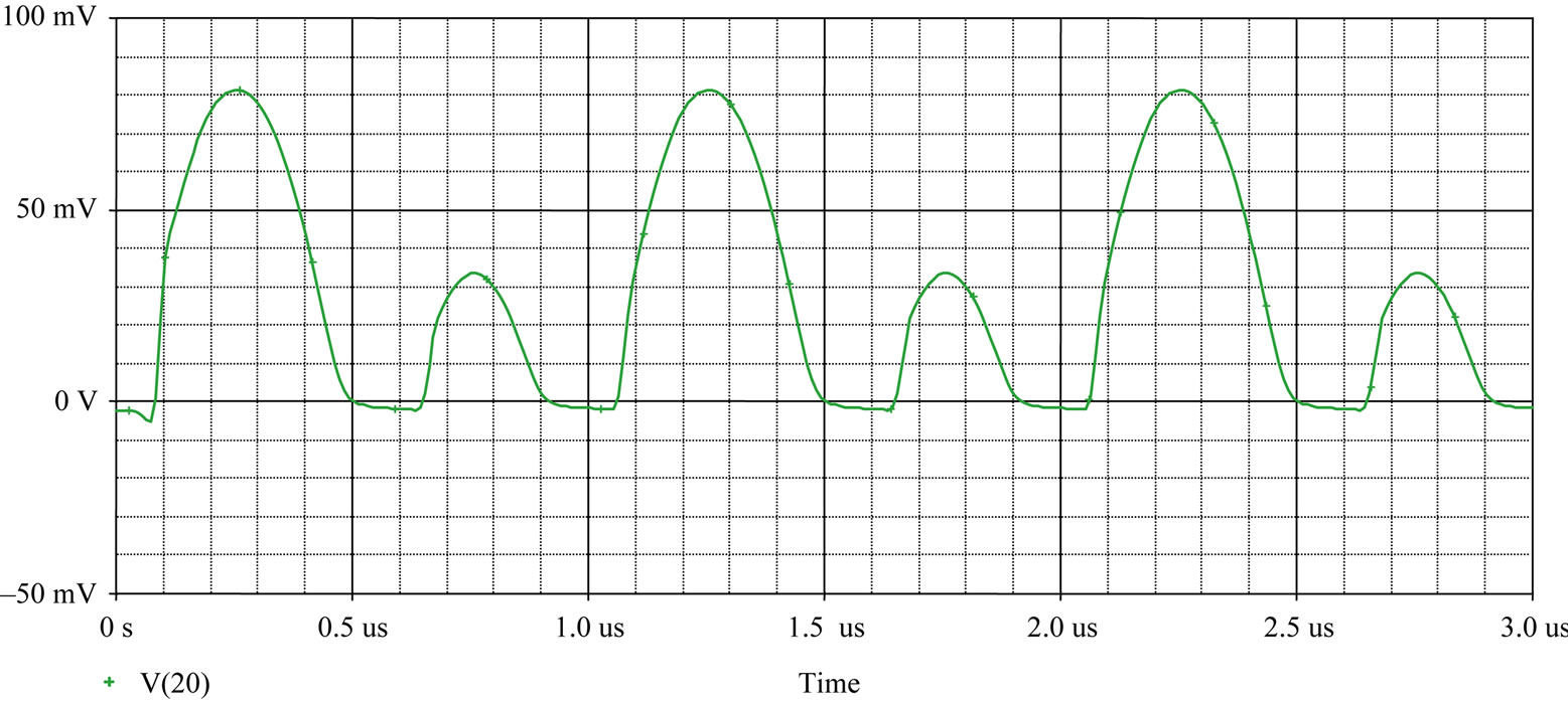
Figure 4. Output of the proposed current-controlled-power full-wave rectifier with an input sine wave, 100 mVpeak, 1 MHz, (ICL+1 = ICL+2 = 1 μA and ICL–1 = ICL–2 = 3.5 μA).

Table 1. Relation between the controlled current and the output.
and current-controlled-power operation. The new rectifier uses all MOSs with typical structure thus it is very suitable for the IC process. The new rectifier, its core operates in balanced mode resulting in a low noise output. Using the new rectifier, one can independently control the positive part and the negative part of the input signal, this yields more precision control.
It should be noted on the use of the new rectifier that it is suitable for a high impedance load. If the low impedance load is applied, it needs a voltage buffer at the output.
REFERENCES
- G. B. Rutkowski and J. E. Oleksy, “Solid-State Electronics,” McGraw-Hill, Singapore, 1992.
- A. Hastings, “The Art of Analog Layout,” Prentice-Hall, Upper Saddle River, 2006.
- B. Razavi, “Design of Analog CMOS Integrated Circuits,” McGraw-Hill, Singapore City, 2001.
- F. W. Hughes, “Op Amp Handbook,” Prentice-Hall, Upper Saddle River, 1993.
- E. Bruun, “CMOS High Speed, High Precision Current Conveyor and Current Feedback Amplifier Structures,” International Journal of Electronics, Vol. 74, No. 1, 1993, pp. 93-100. doi:10.1080/00207219308925816
- Z. Wang, “2-MOSFET Transresistor with Extremely Low Distortion for Output Reaching Supply Voltages,” Electronics Letters, Vol. 26, No. 13, 1990, pp. 951-952. doi:10.1049/el:19900620
- D. Johns and K. Martin, “Analog Integrated Circuit Design,” John Wiley & Sons, New York, 1997.