Circuits and Systems
Vol. 3 No. 1 (2012) , Article ID: 16604 , 7 pages DOI:10.4236/cs.2012.31006
A New Approach to Complex Bandpass Sigma Delta Modulator Design for GPS/Galileo Receiver
Department of Electrical Engineering, Shahid Chamran University, Ahvaz, Iran
Email: nima_ahmadpoor_82@yahoo.com
Received August 14, 2011; revised September 14, 2011; accepted September 22, 2011
Keywords: Continuous Time; Quadrature; Sigma Delta; MOS; Modulator; OTA
ABSTRACT
In this paper, new complex band pass filter architecture for continuous time complex band pass sigma delta modulator is presented. In continuation of paper the modulator is designed for GPS and Galileo receiver. This modulator was simulated in standard 0.18 µm CMOS TSMC technology and has bandwidth of 2 MHz and 4 MHz for GPS and Galileo centered in 4.092 MHz. The dynamic range (DR) is 56.5/49 dB (GPS/Galileo) at sampling rate of 125 MHz. The modulator has power consumption of 4.1 mw with 3 V supply voltage.
1. Introduction
IN recent years, continuous time (CT) sigma delta modulators have attracted increasingly due to low power consumption, low supply voltage, high sampling frequency and high bandwidth in comparison with similar discrete time sigma delta modulators [1-3]. Moreover, because of placing sampler inside loop filter, charge injection effect and nonlinear sampling switched on resistances are significantly suppressed. In addition, the continuous time loop filter attenuating out of band high frequency interferers before sampling act as an anti-alias filter. The CT sigma delta converters have found in such applications as wireless communications systems (zero and low-IF receivers), signal processing, readouts powerless biological signal, in micromachined consumer and professional audio, industrial weight scales and precision measurement devices. Low-IF receivers often use quadrature mixer with complex signals (I/Q) as shown in Figure 1. In the conventional low-IF receivers, analog signal convert to digital by use of two lowpass ADCs, the structure of lowpass ADCs in these receivers lead to interference problems that performed by 1/f noise and DC offset. Even, use of the real bandpass ADC structures in low-IF receivers can be problematic for demanding image rejection requirements and low power consumption although the interferences can be fall outside the signal band. Hence, the quadrature sigma delta modulator is state of the art alternative for the complex analog to digital conversion of quadrature signals in low-IF receivers. In the recent years several successful literatures have been presented, that illustrate the new methods in quadrature bandpass sigma delta design [4,5]. This paper proposes novel design architecture in a bandpass quadrature sigma delta modulator with a lower order and a lower frequency sampling, resulting in low power consumption, the prevention of susceptibility to instability and for goal of smaller chip area. The proposed sigma delta is realized by replacing the lowpass loop filter by complex band pass filter in a lowpass sigma delta, which has been implemented in chain of integrators with feed forward summation (CIFF) topology. The lossy integrators of the design have OTA-C structure with improvement in OTA circuit.
2. Basic Principle of Proposed Complex Filter
Single loop sigma delta architecture often use of several topologies for loop filter, such as chain of integrators with weighted feedforward summation (CIFF) [6], and chain of integrators with distributed feedback (CIFB) [7], resulting in stability and realization considered transfer functions. CIFF topology has several benefits in compared to CIFB. In the CIFF topology the swing of output integrators is lower than CIFB. Consequently, it is better
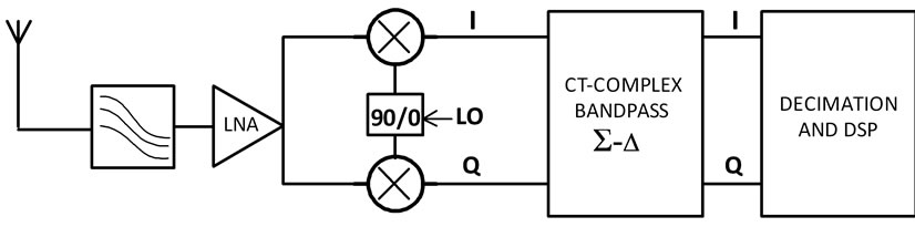
Figure 1. Low-IF receiver structure using complex sigmadelta.
selection for low power, low voltage and wideband modulator implementation. On the other hand, this feature cause to increasing input resistance of integrators, then the unpleasant gain bandwidth effect can be reduced in modulator. Also the CIFF topology have single feedback DAC, which is due to degradation in excess loop delay and clock jitter effects in compared with CIFB. In the proposed design CIFF topology is selected for the complex loop filter architecture of quadrature sigma delta. The transfer function of complex filter is output current to input voltage ratio. So it is transconductance transfer function. For realizing the novel transfer function of complex filter design, one of method is transferring of lowpass filter characteristics from DC to determined center frequency by crass coupling two lowpass filters. So in the first steps we establish the lowpass filter structure. Figure 2 shows the selected lowpass filter with CIFF topology. At the output node, the summation of output feedforward paths is formed with no extra active component circuit. Use of current summation at output node lead to degradation of power consumption and be rising linearity. In the Figure 2, as shown, the output current is collected by summation of transconductance feedforward branches are denoted as gmi (gm1 and gm2). In addition, just as said, the conventional method too shifting transfer function of low pass filter to new center frequency is crass coupling integrators in quadrature paths (I/Q), which is realized the complex filter as shown in Figure 3.
Figure 3 is half structure of the proposed complex filter. As exhibited in Figure 3, crass coupling branches are implemented by transconductances that are denoted as gci, and the basic duty of them is movement poles to center frequency. Furthermore, for the goal of wideband conversion, zeroes of transfer function must be moved to around of center frequency too. This work can be accomplished by feedforward summation coefficients (gmi). In order to optimization of zeros placement, local feedback transconductances are applied, that are named by gbi in Figures 2-3.
3. Implementation
3.1. Operational Transconductance Amplifier (OTA)
Figure 4 shows the optimized OTA from [8]. It can operate in both weak and strong inversion regions and has several benefits, wide common-mode input range, high CMRR and wide linearity limits.
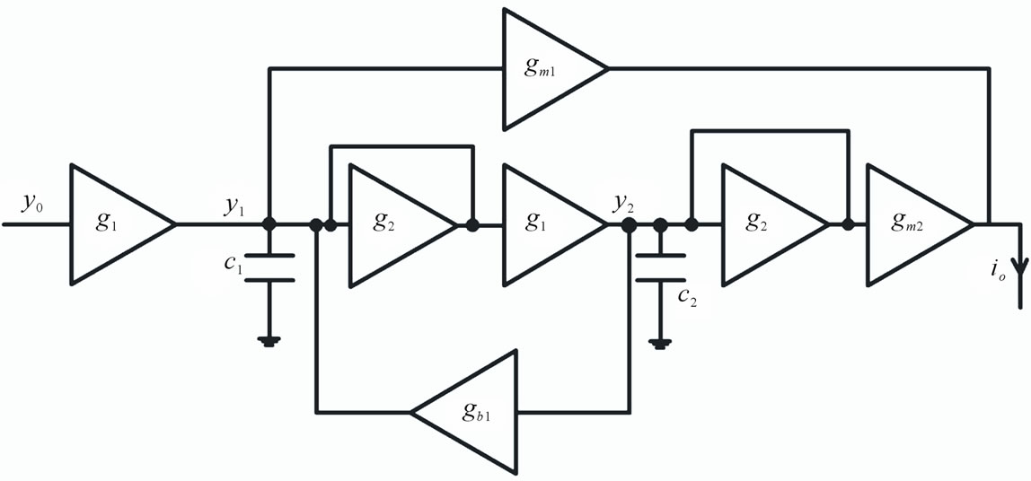
Figure 2. Low-pass filter scheme with CIFF topology.
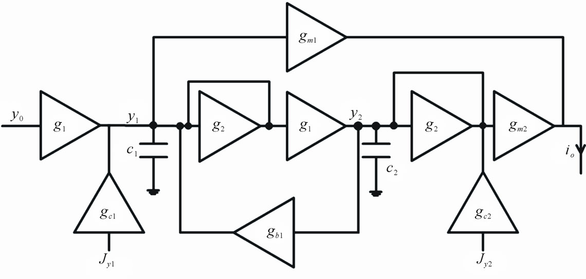
Figure 3. The half structure of the proposed complex filter.
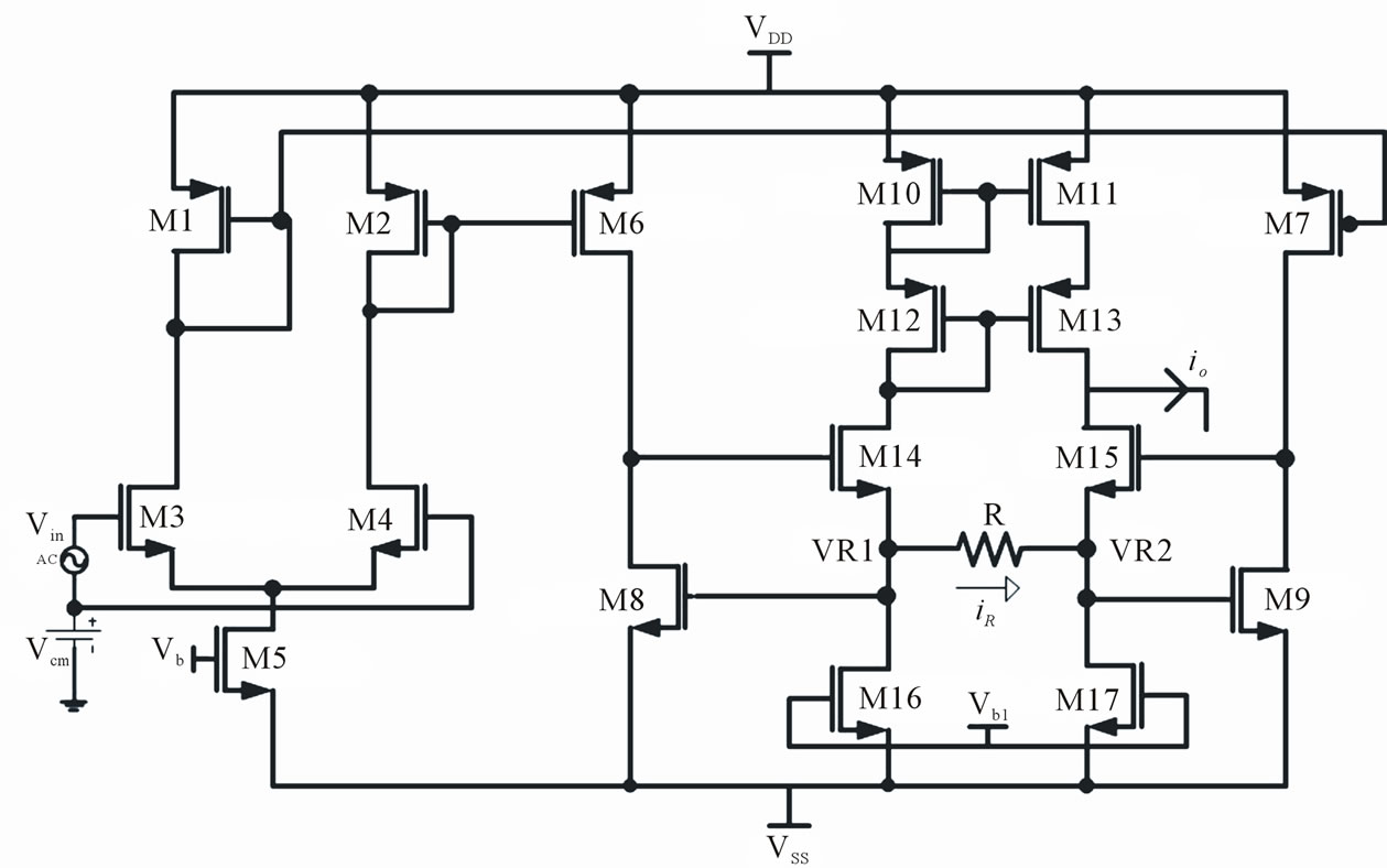
Figure 4. Circuit diagram of the employed OTA.
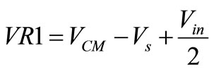
As shown in Figure 4, input common-mode (Vcm) and differential signals (Vin) can be transfer to sides of resistor (R) by transistors M1-M9 with following equations [8]:
 (1)
(1)
 (2)
(2)
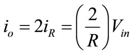
where Vs is voltage of source M1 and M2. From (1) and (2), iR can be obtained by
 (3)
(3)
In circuit schematic of OTA in Figure 4, M10-M13 are operating as current mirrors. Thus, the output current is given by
 (4)
(4)
Above equation indicates the inverse relation between transconductance of OTA and resistor values. Therefore, we can change the transconductor by switching the resistor. This advantage can able us for multi-mode implementation by use of digital calibration logic and external pins.
3.2. Proposed Complex Filter for GPS/Galileo Receivers
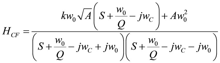
The proposed complex sigma delta modulator can be switched between two satellite navigation systems, for GPS and Galileo. In this receivers, the ADC must support a bandwidth of 2/4 MHz (GPS/Galileo) and the minimum signal to noise ratio (SNR) of 42 dB with an OSR = 64/32 (GPS/Galileo). The center frequency must be tuned in fc = 4.092 MHz. Figure 5 shows the proposed two order complex filter schematic for the GPS/ Galileo modulators, which is useful to low power, low resolution and low data rate. As can be seen in Figure 5, the OTA-C lossy integrators are used for degradation in excess loop delay and mismatch loop delay sensitivity [9]. Furthermore the lossy integrators are used for securing of stability. In this figure Y0 and Q0 are input voltages of complex filter in the quadrature lines, also io and iQ are output currents of complex filter in the quadrature lines. If , the transfer function is:
 (5)
(5)
where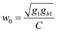 ,
,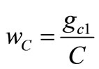 ,
,  ,
, 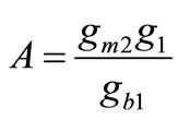 and
and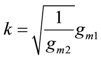 , Parameters of complex filter can be distinguished from the specification the quadrature sigma delta in GPS/Galileo receiver. So the placement of pols of complex filter can be introduced by zeros of the equivalent noise shaping transfer function (NTF). In addition, the crass coupling coefficients can be determined from center frequency of the GPS/Galileo center frequency, and finally the required bandwidth for the GPS/ Galileo sigma delta corresponds to bandwidth and order of complex filter. So the imaging of pols can be determined by
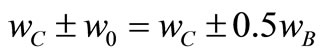 , this relation results:
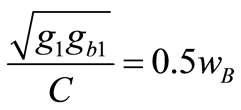 (6)
(6)
The fully proposed circuit of complex filter for GPS/ Galileo bandpass quadrature sigma delta has been shown in Figure 5. That is determined the transconductors and capacitances according to Table 1.
3.3. Quantizer
Figure 6 shows circuit diagram of the applied quantizer. The quantizer consists of a one bit comparator, followed by a D-latch [9]. Two differential amplifiers with diode loads by transistors M1-M10 are used as pre-amplifier and front-end of comparator. Also cross coupled amplifier as a track-and-latch (by transistors M11-M16) is employed for back-end of clocked regenerative comparator. Figure 7 shows circuit diagram of D flip-flap that composed by two back-to-back not gate (transistors M1-M4) for memory cell and another not gate for voltage compatibility of the output (transistors M5, M6). In this Figure  and
and  are output nodes.
3.4. Dac
Figure 8 shows the 1 bit D/A converter that employs two voltage sources and two switches, whose voltages are directed via switches that are controlled by the output of the quantizer. When the switch q turns on, the positive reference voltage connects to the output node and when switch q turns off, the negative reference voltage connects to the output node. In this Figure  and
and  are input nodes and VD/C is output node.
4. Simulation Result
The proposed second order complex bandpass sigmadelta modulator circuit was simulated by HSPICE in 0.18 µm CMOS TSMC technology. Vdd = 1.5 V, Vss = –1.5 V and Vref = ±0.9 V was chosen. Two sinusoidal quadrature signals with amplitude of 0.5 Vref and frequency of 4 MHz were applied for input of modulator. The sampling frequency was set 125 MHz the oversampling ratios (OSR), are 64/32(GPS/Galileo). The bandwidth is switched for GPS/Galileo by change of transcondutor values in local feedback loop and lossy integrators, as shown in Table 1, as well as the bandwidth can be tuned by switchable integrating capacitors and center frequency can be tuned by crass coupling transcondutor values, which can be change by replacing resistor of proposed OTA whit logic switches and external pins. The output data of the modulator were collected, and then 50 kHz fast Fourier transformation (FFT) with hanning window was used to evaluate SNR and power spectral density (PSD). Figure 9 shows the power spectrum of the GPS modulator and Figure 10 shows Signal-to-Noise vs. input amplitude for the GPS/Galileo receiver, this figure
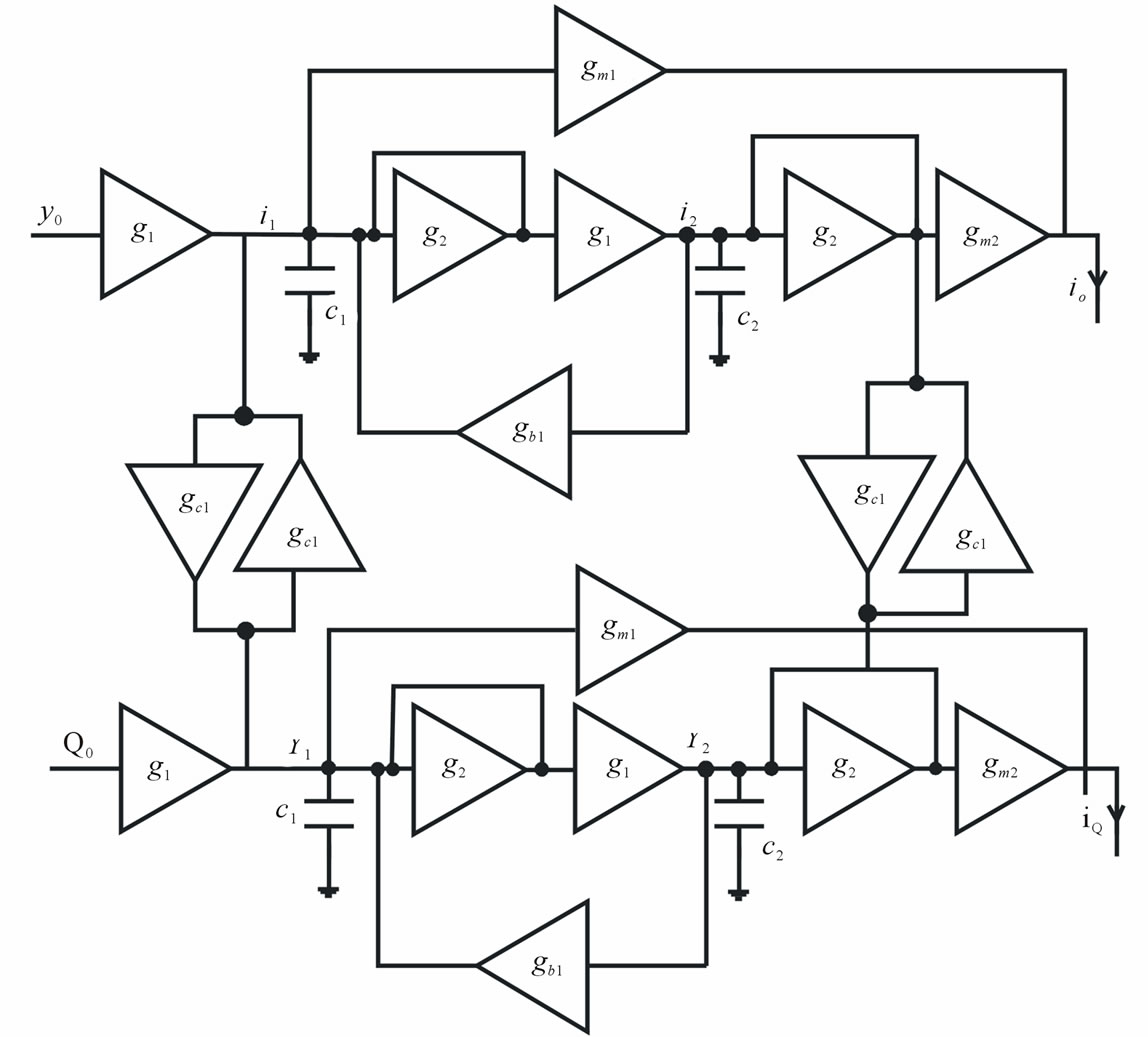
Figure 5. Fully schematic of the proposed complex filter.
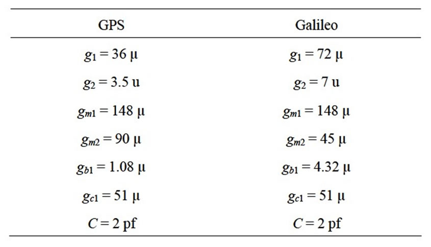
Table 1. Component values of the proposed complex filter.
shows that the maximum SNR (including distortion) for the GPS and Galileo modulators are 52 dB and 47 dB respectively, therefore the bit resolution of proposed modulator is 8.3 bit and 7.5 bit respectively. Furthermore we can determine the dynamic range of modulators from Figure 10; these values are 56.5 dB and 49 dB for the GPS and Galileo modulator respectively. Simulation results showed the power consumption of less than 4.1mW. The characteristics of the modulator for the GPS/Galileo are summarized in Table 2. Also this design compare with two same recent works too. As seen in the last row of table, the figure of merit was used for comparison of
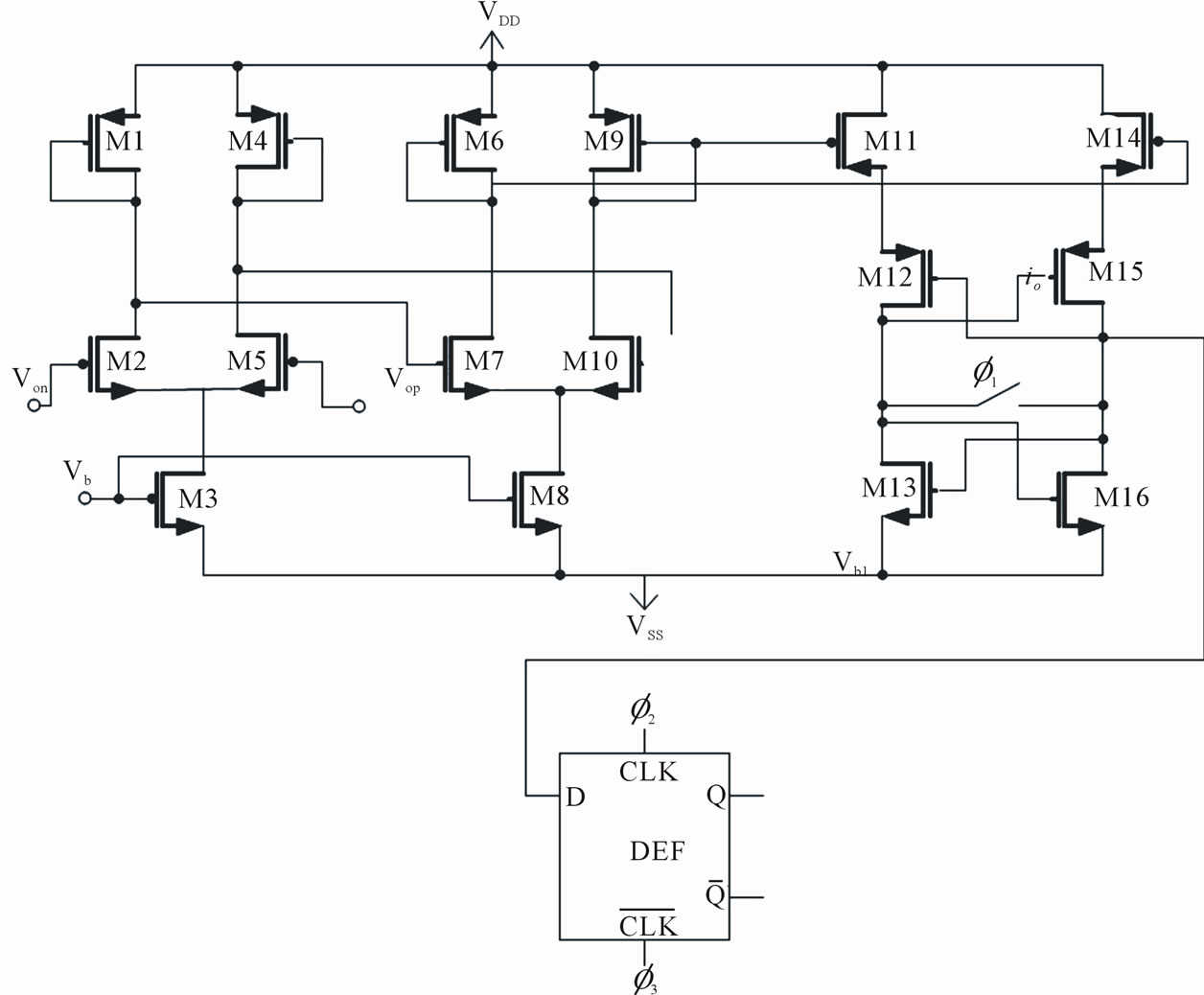
Figure 6. Circuit diagram of the applied quantizer.

Figure 7. Circuit diagram of D flip-flap.
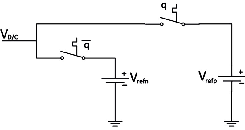
Figure 8. Circuit diagram of the 1bit D/A converter.
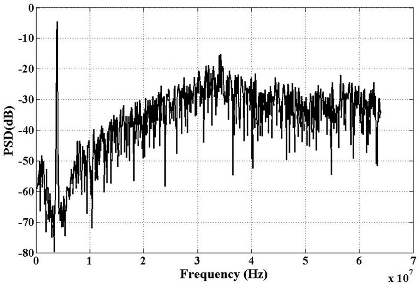
Figure 9. Power spectrum of the modulator.
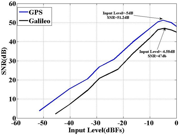
Figure 10. Signal-to-Noise vs. input amplitude of the modulator.
performances that is certifying to preference of this design. This figure of merit is calculated by following formula:
 (7)
(7)
5. Conclusion
A new continuous time complex bandpass sigma delta modulator for using multi-mode receiver (GPS/Galileo) is presented. The modulator was realized in new structure
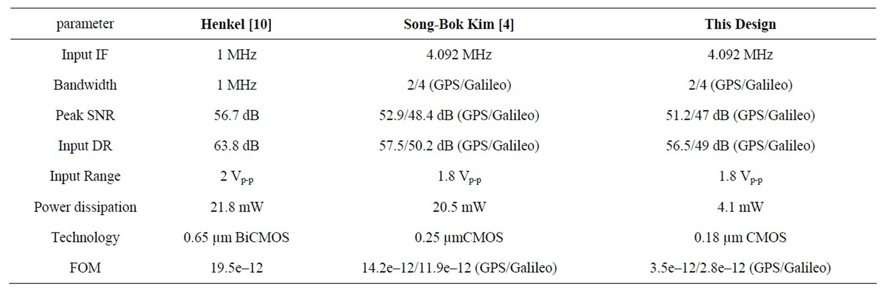
Table 2. Circuit charactristic.
with CIFF topology and transconductance transfer function. So it was designed for the low power consumption. The proposed complex modulator has 4.1 mw power consumption at ±1.5 supply voltage. It can provide the peak SNR 51.2 dB and 47 dB and a dynamic range of 56.5 dB and 49 dB at Fs = 125 MHz for the GPS and Galileo respectively.
REFERENCES
- E. D. Gioia and H. Klar, “A 11-bit, 12.5 MHz, Low Power Low Voltage Continuous-Time Sigma-Delta Modulator,” Proceedings of the 17th International Conference on Mixed Design of Integrated on Circuits and Systems (MIXDES), Warsaw, 24-26 June 2010, pp. 176-181.
- G. Mitteregger, C. Ebner, C. Mechnig, T. Blon, C. Holuigue, E. Romani, A. Melodia and V. Melini, “A 14b 20 mW 640 MHz CMOS CT/spl Delta//spl Sigma/ADC with 20 MHz Signal Bandwidth and 12b ENOB,” Solid-State Circuits Conference (ISSCC), Digest of Technical Papers IEEE International, San Francisco, 6-9 February 2006, pp. 131-140.
- E. Prefasi, L. Hernandez, S. Paton, A. Wiesbauer, R. Gaggl and E. Pun, “A 0.1 mm, Wide Bandwidth ContinuousTime ADC Based on a Time Encoding Quantizer in 0.13 m CMOS,” IEEE Journal of Solid-State Circuits, Vol. 44, No. 10, 2009, pp. 2745-2754. doi:10.1109/JSSC.2009.2027550
- S. B. Kim, S. Joeres, N. Zimmermann, M. Robens, R. Wunderlich and S. Heinen, “Continuous-Time Quadrature Bandpass Sigma-Delta Modulator for GPS/Galileo Low-IF Receiver,” IEEE International Workshop on Radio-Frequency Integration Technology (RFIT 007), Rasa Sentosa Resort, 9-11 December 2007, pp. 127-130. doi:10.1109/RFIT.2007.4443935
- J. Arias, P. Kiss, V. Prodanov, V. Boccuzzi, M. Banu, D. Bisbal, J.S. Pablo, L. Quintanilla and J. Barbolla, “A 32-mW 320-MHz Continuous-Time Complex DeltaSigma ADC for Multi-Mode Wireless-LAN Receivers,” IEEE Journal of Solid-State Circuits, Vol. 41, No. 2, 2006, pp. 339-351. doi:10.1109/JSSC.2005.862346
- F. Esfahani, P. Basedau, R. Ryter and R. Becker, “A Fourth Order Continuous-Time Complex Sigma-Delta ADC for Low-IF GSM and EDGE Receivers, in VLSI Circuits,” Symposium on Digest of Technical Papers, 12- 14 June 2003, pp. 75-78.
- M. Ortmanns, F. Gerfers and Y. Manoli, “A ContinuousTime Sigma-Delta Modulator with Switched Capacitor Controlled Current Mode Feedback,” Proceedings of the 29th European Solid-State Circuits Conference (ESSCIRC’ 03), 16-18 September 2003, pp. 249-252.
- K. Tanno, H. Tanaka, R. Miwa and H. Tamura, “WideCommon-Mode-Range and High-CMRR CMOS OTA Operable in Both Weak and Strong Inversion Regions,” IEEE Asia Pacific Conference on Circuits and Systems (APCCAS), Macao, 30 November-3 December 2008, pp. 1180-1183.
- S. B. Kim, S. Joeres and S. Heinen, “A Compensation Method of the Excess Loop Delay in Continuous-Time Complex Sigma-Delta Modulators,” 18th European Conference on Circuit Theory and Design (ECCTD), Seville, 27-30 August 2007, pp. 140-143. doi:10.1109/ECCTD.2007.4529556
- F. Henkel, U. langmann, A. Hanke, S. Heinen and E. Wagner, “A 1-MHz-Bandwidth Second-Order Continuous-Time Quadrature Bandpass Sigma-Delta Modulator for Low-IF Radio Receivers,” IEEE Journal of SolidState Circuits, Vol. 37, No. 12, 2002, pp. 1628-1635. doi:10.1109/JSSC.2002.804332