Journal of Signal and Information Processing
Vol. 4 No. 2 (2013) , Article ID: 30993 , 6 pages DOI:10.4236/jsip.2013.42017
Design of a Low-Noise Front-End Readout Circuit for CdZnTe Detectors*
![]()
School of Computer Science and Technology, Northwestern Polytechnical University, Xi’an, China.
Email: shykongxin@163.com
Copyright © 2013 Bo Gan et al. This is an open access article distributed under the Creative Commons Attribution License, which permits unrestricted use, distribution, and reproduction in any medium, provided the original work is properly cited.
Received January 9th, 2013; revised February 11th, 2013; accepted February 22nd, 2013
Keywords: CdZnTe; Detector; Low Noise; Front-End; Readout; CMOS
ABSTRACT
In this paper, the design of a novel low-noise front-end readout circuit for Cadmium zinc telluride (CdZnTe) X-ray and γ-ray detectors is described. The front-end readout circuits include the charge sensitive amplifier (CSA) and the CR-RC shaper is implemented in TSMC 0.35 μm mixed-signal CMOS technology. The die size of the prototype chip is 4.9 mm × 2.2 mm. The simulation results show that, the noise performance is 46 electrons + 10 electrons/pF, and power consumption is 1.65 mW per channel.
1. Introduction
Cadmium zinc telluride (CdZnTe) crystal [1] is a new semiconductor material which has a high performance in the radiation environment at room-temperature. The CdZnTe detectors, which have several significant advantages such as high stopping power, good energy resolution and high spatial resolution, are one of the principal detector materials for the next-generation X-ray imager and γ-ray imager. In the present, a number of internationally renowned research institutions and universities are actively using these detector systems to carry out research in the areas of medical imaging, illicit substance detection and materials characterization [2,3].
As the most important part of the detector system, the low noise front-end readout circuits would have an important impact for the performances of the whole system. Since the CdZnTe detectors are usually used for the detection of X-ray and γ-ray, the input signals, which would be processed by the readout circuit, should exist in a high bandwidth. And the minimum signal must be an extremely weak signal. In order to ensure the signal to noise ratio (SNR) and sufficient range of the output signal, the front-end readout circuits with very low-noise and very high gain are necessary. For these two requirements, the low-noise design is the most important in the various performance requirements [4].
In this paper, the design of the front-end readout circuit for CdZnTe detectors is implemented in TSMC 0.35 μm mixed-signal CMOS technology. We have designed a 32- channel chip, each channel consists of a charge sensitive amplifier (CSA), a CR-RC shaper amplifier and an output buffer (Figure 1).
Figure 1. Schematic of the front-end system.
Compared to the existing designs, in this paper, we improved the circuits of preamplifier and shaper. And an ultra low-noise front-end readout circuit has been achieved. When the detector capacitor was 5 pF, and the output SNR is greater than 10, the minimum value of input signal can be reached to 1000 electrons.
2. Preamplifier Design
The noise performance at the output of a preamplifier is determined by two factors: the intrinsic noise generated by the preamplifier itself and the noise of the detector [6]. Therefore, low noise preamplifier design would be achieved considering preliminary minimization of the intrinsic noise of the preampli-fier and then obtaining the optimal noise matching condition in the preamplifier for the given detector.
Both the optimal noise matching condition and the intrinsic noise contribution of the preamplifier are principally determined by the input transistor. In this paper, we choose a NMOS input transistor.
The noise performance of the input stage is characterized by the equivalent noise voltage source  [7]:
[7]:
 (1)
(1)
In Equation (1), we can see that the circuit noise is built up from the thermal noise of channel and the flicker noise of input transistor. As a result, we could keep Kf as small as possible in order to reduce noise. In TSMC 0.35 μm CMOS technology, Kf of the NMOS transistors is , and the value of PMOS transistors is
 . In order to minimize the intrinsic noise, a NMOS input transistor should be chosen with a smaller value of Kf.
Also, if choosing a PMOS transistor as input, in order to reduce the effect by the power supply noise we have to make the source of input transistor connect to ground. Therefore it is necessary to use a pair of positive and negative voltages as VDD and VSS, so we need 3 power supplies, thus increasing the design difficulty of the I/O cell and ESD circuits. Moreover, using VDD, VSS and GND at the same time is not conducive to integrate follow-up digital circuits into the chip using VDD, VSS and GND at the same time is not conducive to integrate follow-up digital circuits into the chip The core of the preamplifier is implemented with a single-ended input split-leg cascode configuration shown in Figure 2. A large bias current would through the input device to achieve large transconductance, which is necessary for fast rise time. However, the bias current in the output leg should keep low in order to provide high impedance for high open-loop gain.
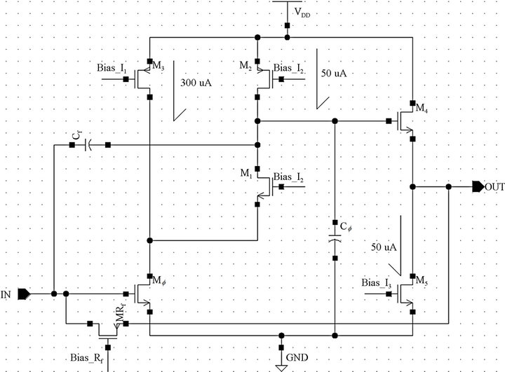
Figure 2. Schematic of preamplifier.
Comparing the two cascode configurations shown in Figure 3, we can see that a split-leg straight cascode configuration is better than the folded cascode counterpart [8]. Because it maximizes the current in the input transistor by summing the current in both legs for highest gm while also providing high impedance at the output node. However, bias current in the output leg must be large enough to avoid that a slew-rate limited response for a large capacitive load at the amplifier output.
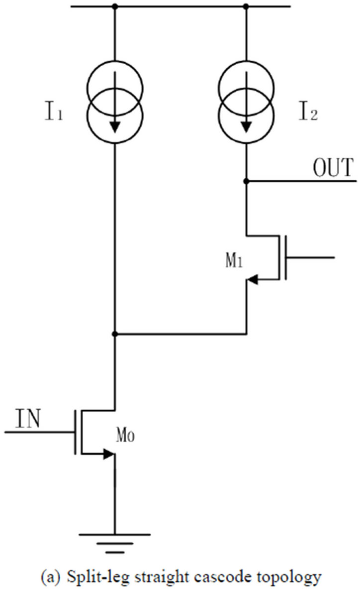
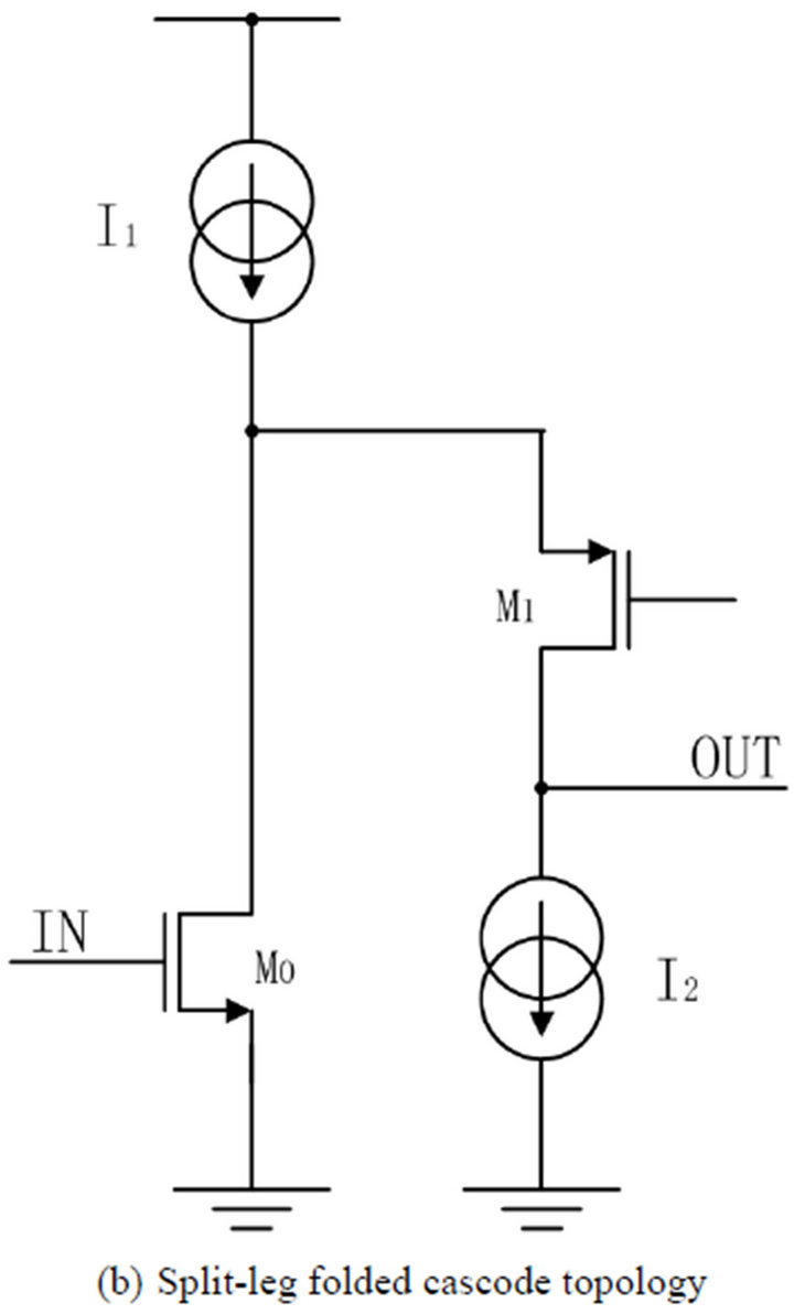
Figure 3. Two different cascode configurations.
In the folded topology, we usaully choose a PMOS transistor as M1 in order to get the best performance. It is desirable to keep M1 small to reduce the capacitance at its drain and source that are connected to the sensitive high-impedance output node which contributes dominant pole and the split node that contributes the critical second pole. But at the same time, M1 should be large enough to keep the resistance looking into its source small [9]. In other words, to satisfy these two conflicting requirements, we must maximize the transconductance to capacitance ratio of M1. Therefore, M1 should be a NMOS transistor, because it yields higher gm, particularly in strong inversion region, and lower junction capacitance due to lower doping profiles, than a PMOS transistor.
The preamplifier’s main design parameters are given in Table 1.
3. Shaper Design
In Equation (1) we can see that when the transistor is determined, in different frequency domain, the thermal noise of amplifier is fixed, and the flicker noise should be reduced as the frequency increases. Figure 4 shows the circuit noise in different frequency. If the frequency closes to 0, the flicker noise will be very large. It will significantly affect the overall circuit noise performance.
As a result, it is necessary to insert a shaper following the preamplifier. In the frequency domain the shaper can be considered as an active band-pass filter, which is used to limit the input signal bandwidth from the charge sensitive amplifier, to reduce the gain in low-frequency (therefore reduce the low frequency noise), and to increase the signal to noise ratio S/N of the system.
By calculating and comparing, for the preamplifier of this design, when the shaping time Tp is close to 1.5 μs, we can get the best noise filtering effect. Not only the flicker noise will be significantly reduced, but also the thermal noise will not be introduced too much. In this design, we have chosen a PMOS transistor as the feedback resistance Rfs in order to adjust the shaping time.
The schematic of the shaper’s core amplifier is same to the one of preamplifier. The only difference is that they have different transistor dimensions. The focus of shaper design is to adjust the value of coupling CR and feedback CR, in order to change the shaping time and gain of shaper.

Table 1. Main design parameters of the preamplifier.

Figure 4. Noise of preamplifier vs. the frequency.
The main design parameters of shaper are shown in Table 2.
4. Experimental Results and Discussions
In order to investigate the features of the front-end readout circuit designed above, we have made a simulation by SPECTRE. The input signals are current pulses, such as a pulse of 80 nA during 40 ns, the charges of this pulse is about 20,000 electrons.
Assuming 5 pF detector capacitance and 20,000 electrons input charges, the simulation results of the readout circuit’s output signal is shown in Figure 5. By calculating and measuring, we can get the following results. The gain of readout system is 4 mV/pC, the power consumption is less than 1.65 mW, and the shaping time can be adjusted from 1 μs to 3 μs.
The noise of the chip has been simulated by the following methods. The output voltage fluctuation of a single channel is measured. The equivalent noise charge (ENC) with an input stray capacitance can be determined when the input level is known. Layout of one channel and bias circuit is shown in Figure 6. And then, measure the average of the ENC for different channel and same detector capacitor in a multi-channel design. Layout of
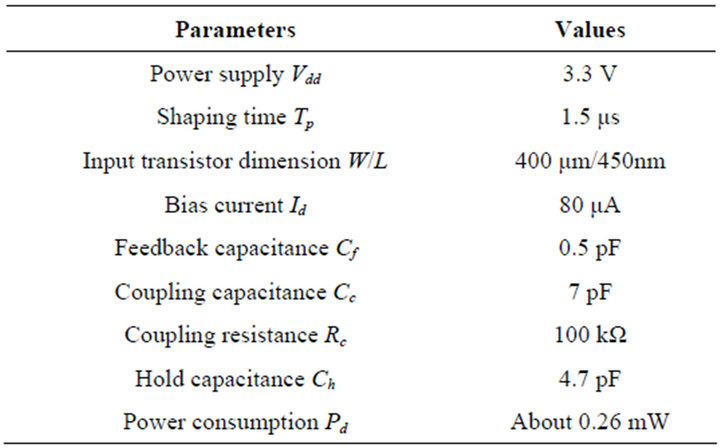
Table 2. Main design parameters of the shaper.
the 32-channel readout system is shown in Figure 7. The results are presented in Figure 8. Based on the above measurement, we get a convergent result. It shows that the noise performance was 46 electrons for a 0 pF detector capacitance with a slope of 10 electrons/pF.
5. Conclusion
In this paper, a low noise readout circuit for CdZnTe detector has been presented. The simulation results show that, a noise performance of 
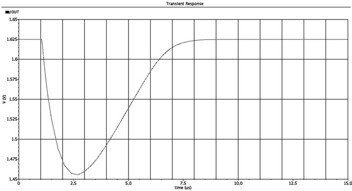
Figure 5. Output signal of front-end readout circuit.
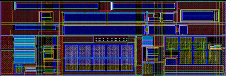
Figure 6. Layout of 1-channel readout and bias circuits.

Figure 7. Layout of 32-channel readout system.
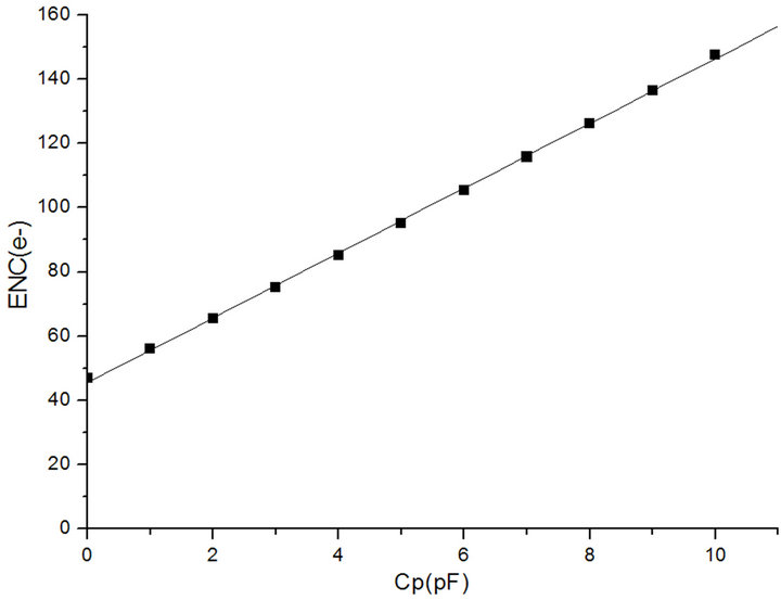
Figure 8. Circuit noise performance vs. detector capacitor.
can be obtained with a power consumption of 1.65 mW per channel for a shaping time of 1.5 μs, and this design can be used in multi-channel detector readout systems. The results show us a reasonable possibility for X-ray and γ-ray imaging to detect above 1000 electrons. And this kind of CdZnTe front-end readout circuits can be widely used in particle physics, nuclear physics, X-ray detection and γ-ray detection.
REFERENCES
- M. Amman, J. S. Lee, P. N. Luke, H. Chen, S. A. Awadalla, R. Redden and G. Bindley, “Evaluation of THMGrown CdZnTe Material for Large-Volume Gamma-Ray Detector Applications,” IEEE Transactions on Nuclear Science, Vol. 56, No. 3, 2009, pp. 795-799. doi:10.1109/TNS.2008.2010402
- L. L. Jones, P. Seller, M. Wilson and A. Hardie, “HEXITEC ASIC-A Pixellated Readout Chip for CZT Detectors,” Nuclear Instruments and Methods in Physics Research Section A, Vol. 604, No. 1-2, 2009, pp. 34-37. doi:10.1016/j.nima.2009.01.046
- O. Lazzari, S. Jacques, T. Sochi and P. Barnes, “Reconstructive Color X-ray Diffraction Imaging—A Novel TEDDI Imaging Method,” RSC Analyst, Vol. 134, No. 9, 2009, pp. 1802-1807. doi:10.1039/b901726g
- E. Beuville, K. Borer, E. Chesi, E. H. M. Heijine, P. Jarron, B. Lisowski and S. Singh, “AMOLEX, a Low-Noise, Low-Power Analog CMOS Signal Processor for MultiElement Silicon Particle Detectors,” Nuclear Instruments and Methods in Physics Research, Vol. A288, No. 1, 1990, pp. 157-167.
- L. T. Wurtz and W. P. Wheless Jr., “Design of a HighPerformance, Low Noise Charge Preamplifier,” IEEE Transactions on Circuits and Systems, Vol. 40, No. 8, 1993, pp. 541-545, doi:10.1109/81.242329
- Y. Hu, W. Dulinski, R. Turchetta, J. Kaplon, J. Ph. Blonde and M. Schaeffer, “Design of a Low Noise, SelfTriggered, Monolithic Preamplifier Dedicated to Silicon Trackers and X-β Imaging,” Nuclear Instruments and Methods in Physics Research Section A, Vol. 361, No. 13, 1995, pp. 568-573. doi:10.1016/0168-9002(95)00208-1
- Z. Chang and W. M. Sansen, “Low-Noise, Low-Distortion CMOS AM Wide-Band Amplifiers Matching a Capacitive Source,” IEEE Journal of Solid-State Circuits, Vol. 25, No. 3, 1990, pp. 833-840. doi:10.1109/4.102682
- M. Weng, E. Mandelli, W. W. Moses and S. E. Derenzo, “A High-Speed Low-Noise 16-Channel Charge-Sensitive Preamplifier ASIC for APD-Based PET Detectors,” IEEE Transactions on Nuclear Science, Vol. 50, No. 4, 2003, pp. 898-902. doi:10.1109/TNS.2003.814565
- K. T. Z. Oo, E. Mandelli and W. W. Moses, “A HighSpeed Low-Noise 16-Channel CSA with Automatic Leakage Compensation In 0.35-um CMOS Process for APDBased PET Detectors,” IEEE Transactions on Nuclear Science, Vol. 54, No. 3, 2007, pp. 444-453. doi:10.1109/TNS.2007.893326
NOTES
*This work is supported by the National Natural Science Foundation of China (No. 60972157 and No. 61101190).