Journal of Sensor Technology
Vol.2 No.3(2012), Article ID:22872,6 pages DOI:10.4236/jst.2012.23019
Modelling of Thermal Behavior N-Doped Silicon Resistor
1Modeling of Energy Renewable Devices and Nano-Metric Laboratory, University of Mentouri, Constantine, Algeria
2Laboratory of Architecture and Systems Analysis, National Centre of Scientific Research, Toulouse, France
Email: f_kerrour@yahoo.fr
Received June 14, 2012; revised July 15, 2012; accepted August 16, 2012
Keywords: Silicon; TCRs; Mobility; Doping; Temperature
ABSTRACT
From the analysis of the frequently models of mobility used in the literature, we determine by an identification method the temperature coefficients α and β of a silicon resistance doped with donor atoms. Their variations show a non linear dependence according to the doping and the existence of a minimal value at particular concentration. Moreover, the comparison between the obtained results and those of a P-type resistance shows that there is a strong similarity in their thermal behaviours, except for a particular couple of α and β.
1. Introduction
The increasingly miniaturization and integration require, for the modeling engineers and manufacturers of integrated circuits, to improve the behavioural models of the electronic components. Among the latter, semiconductor resistors are used in all components either as passive elements of an electronic circuit or as a sensor (pressure, temperature, chemical species, etc.). In all cases, and in order to preserve the integrity of the useful signal, their sensitivity to the influence parameters must be sufficiently well-known and controlled, either in an empirical way, or by analytical laws. Whatever the purpose of their use or their operating mode, the thermal resistance behaviour must be apprehended in the most accurate way. In a previous study [1], we showed that the thermal drift of a silicon resistor doped with acceptors atoms could be described by an equation of the second order and that the two temperature coefficients (TCRs) have a strong dependence with the doping concentration. Following the same idea, we modelled the influence of the doping concentration on the temperature coefficients of a resistor doped with donor atoms. Knowing that there are differences between the laws controlling the mobility of the electrons and the holes, one can expect that the resistivity of this material shows different behaviour according to the doping type.
2. Relation Resistivity-Mobility
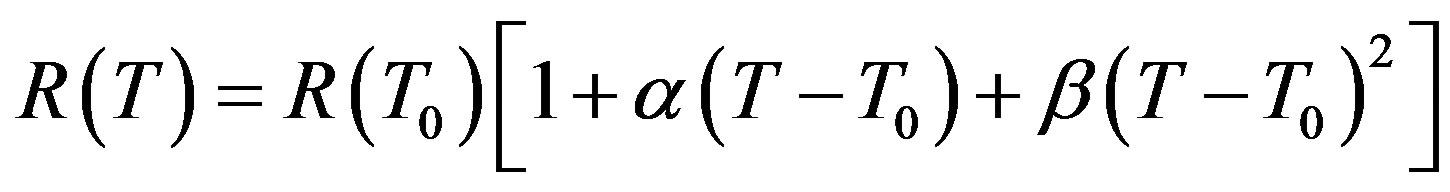
The expression of a silicon resistance according to the temperature T is given by
 (1)
(1)
where  is a reference temperature; α and β are the first and second order TCRs.
Knowing that [1]:
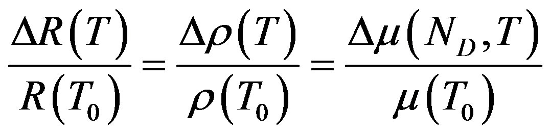 (2)
(2)
where ρ and µ are respectively the silicon resistivity and the carriers’ mobility, it would be sufficient to model the carriers’ mobility behaviour according to temperature and doping to obtain the expressions of the two coefficients (TCRs). So far, no analytical model allows us to describe this dependence. On the other hand, there are several empirical models describing the influence of doping and the temperature on the carriers mobility, among which we used those of Arora [2], Klaassen [3] and Dorckel [4] as is shown in the Appendix. In order to evaluate the total carrier mobility (µi for electron and µj for hole), we use the Mathiessen’s rule which approximates it at low longitudinal field as the sum of four term, which are the four contributions to the carrier mobility: Lattice mobility (µi, L); donor mobility (µi, D); acceptor mobility (µi, A) and electron-hole scattering mobility (µi, j), and includes temperature dependence [5,6]:
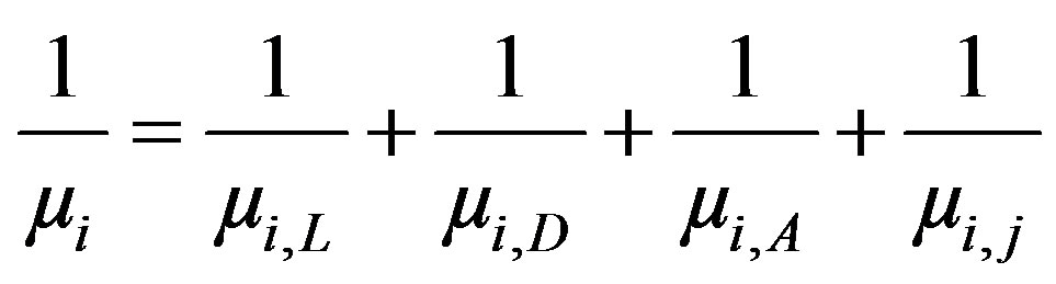 (3)
(3)
Thus, using a limited development of the mobility’s expressions µ = f(ND, T) taken from these references, we used a method of parameters identification. This method is a term by term comparison of the mobility expression as a function of temperature, with Equation (2), for each concentration. Thus, we obtain the expression of α = f(ND) and β = f(ND).
3. Results
The obtained results allowed us to plot the curves in Figures 1 and 2. These figures show that for the three models, there is a strong similarity in the shape of the nonlinear curves α = f(ND) and β = f(ND). Moreover, the shapes of these curves are similar to those published in [1], as shown in Figures 3 and 4; moreover the minimum values appear for a given doping.
The comparison between the results previously published for a P-type resistor (Figures 3 and 4) and those studied in this work (Figures 1 and 2) should allow to quantify their respective thermal drifts as a function of the doping concentration in one hand, and on the other hand, to validate or not the non linear approach of their thermal coefficients (TCRs) in a given temperature range. Thus, by using the minimal values of the coefficients α and β taken from the curves in Figures 1-4, and by their substitution in the Equation (2), we plotted the curves of the relative resistance variation  as a function of the temperature variation ΔT for the two types of doping
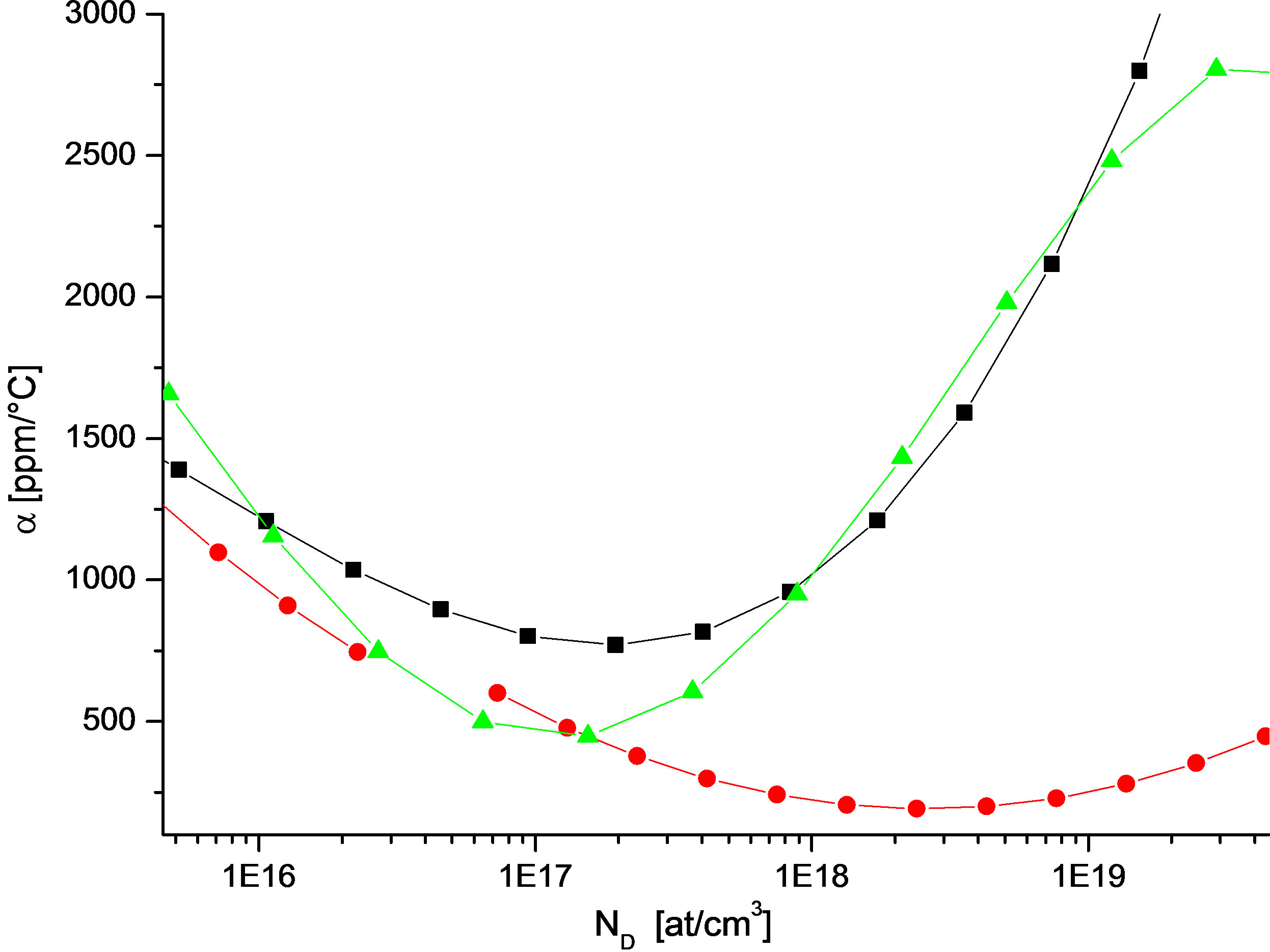
Figure 1. Variations of the first order thermal coefficient α as a function of doping concentration ND.  Klaassen; αmin = 445 ppm/˚C;
  Arora; αmin = 770 ppm/˚C;
  Dorckel; αmin = 190 ppm/˚C.
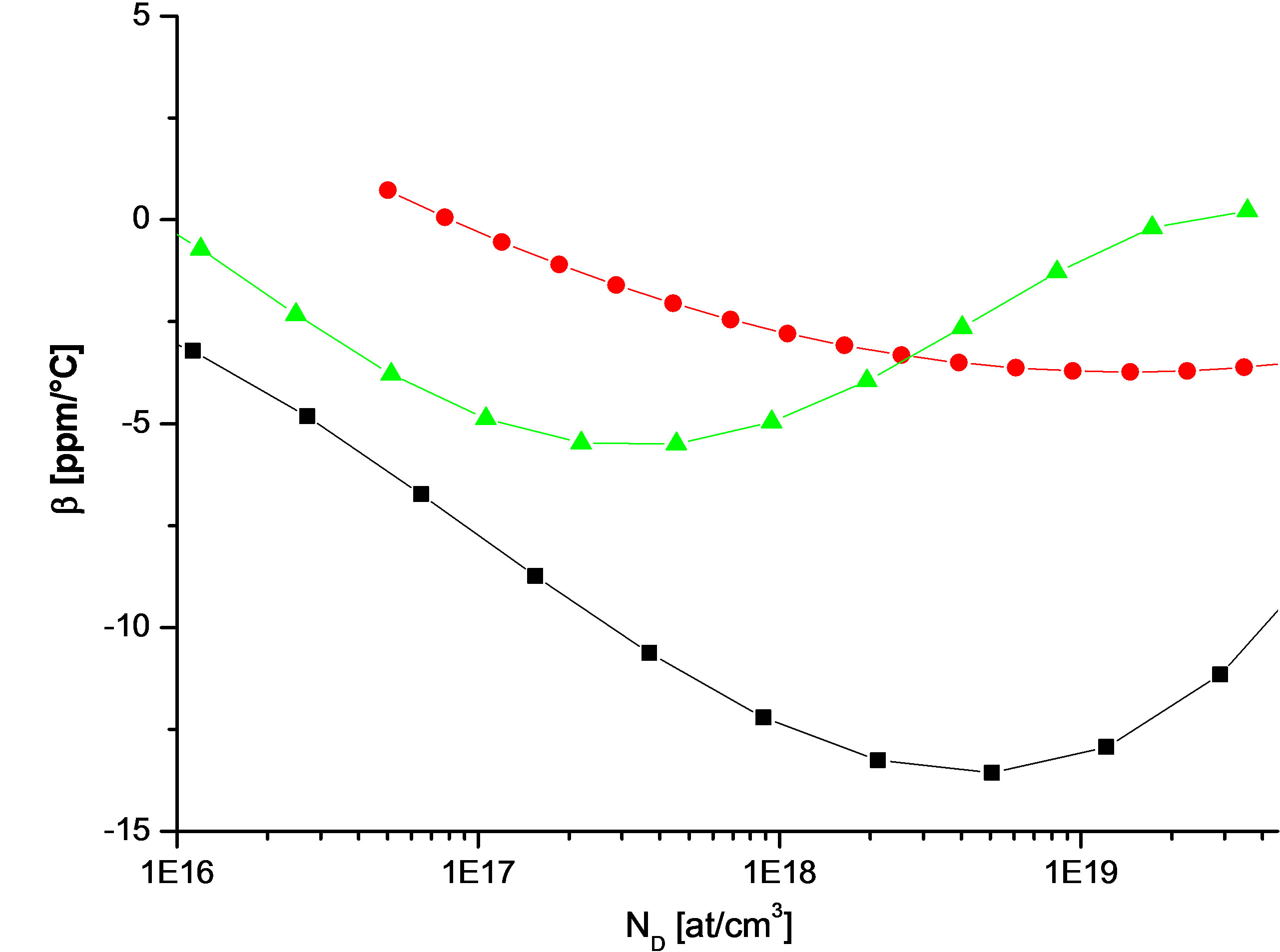
Figure 2. Variations of the second order thermal coefficient β as a function of doping concentration ND.  Dorckel; βmin = –3.80 ppm/˚C;
  Klaassen; βmin = –5.00 ppm/˚C;
  Arora; βmin = –13.6 ppm/˚C.
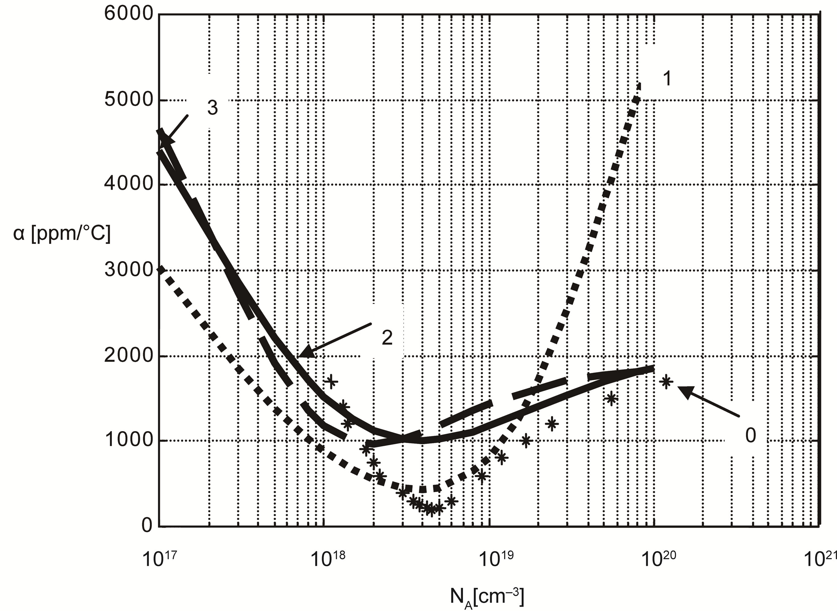
Figure 3. Variations of the first order thermal coefficient α as a function of doping concentration NA [1]. 0: Bullis [6] αmin = 200 ppm/˚C; 1: Dorckel [4] αmin = 400 ppm/˚C; 2: Arora [2] αmin = 980 ppm/˚C; 3: Klaassen [3] αmin = 1000 ppm/˚C
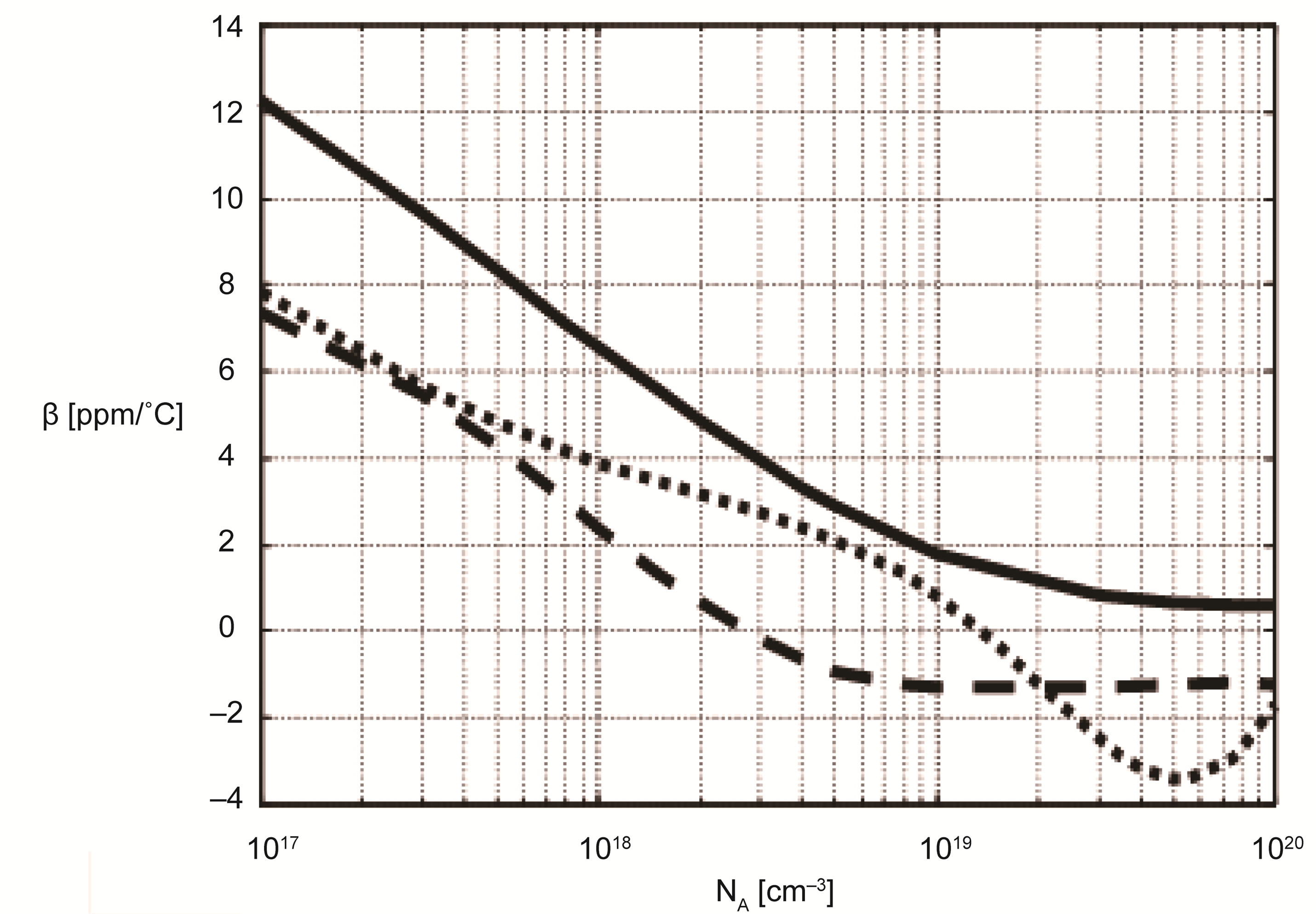
Figure 4. Variations of the second order thermal coefficient β as a function of doping concentration NA[1].
(Figure 5 for the type P; Figure 6 for the type N). Since the minimum value for different models do not occur at the same doping concentration for the α parameter than for the β one, then we have choose, for a same doping concentration, particular coefficients couples (αmin, β).
These values are used to evaluate the relative resistance change  as a function of the temperature variation ΔT. The minimum values of the first and second order thermal coefficients were determined in order to predict the variation of the P-type and the N-type thermal drift resistance, for a given doping concentration.
Figure 5 shows clearly that for a couple αmin(NA) and βmin(NA) for the P-type resistor thermal variations can be considered as linear in a large interval of temperature. Figure 6 shows that the N-type resistor thermal behavior is highly nonlinear, whatever the values of αmin(ND) and βmin(ND). Therefore, these results may help the more complicated circuits to choose the resistors doping con
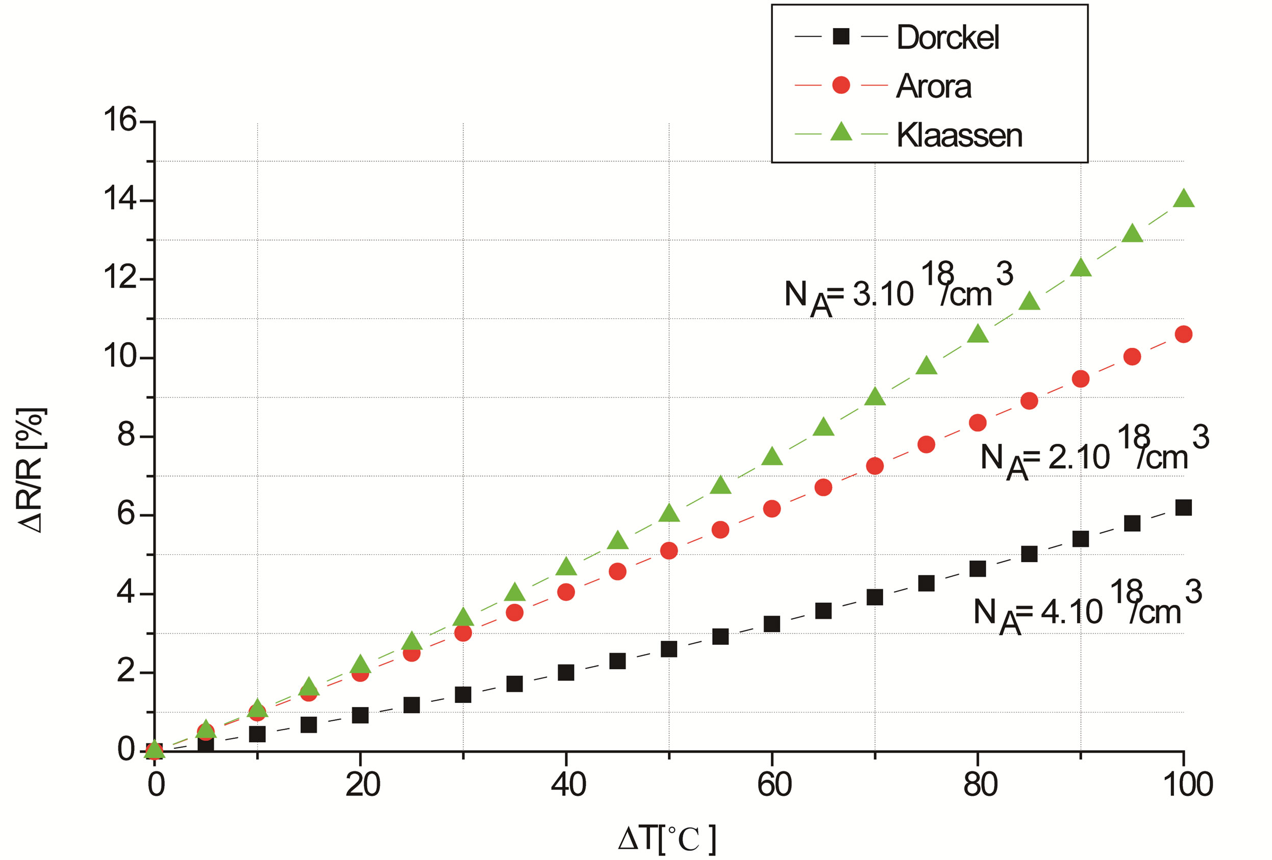
Figure 5. Variations of the relative resistance  as a function of the temperature gradient ΔT for a particular couple (αmin(NA), β min(NA)), for a given doping concentration.
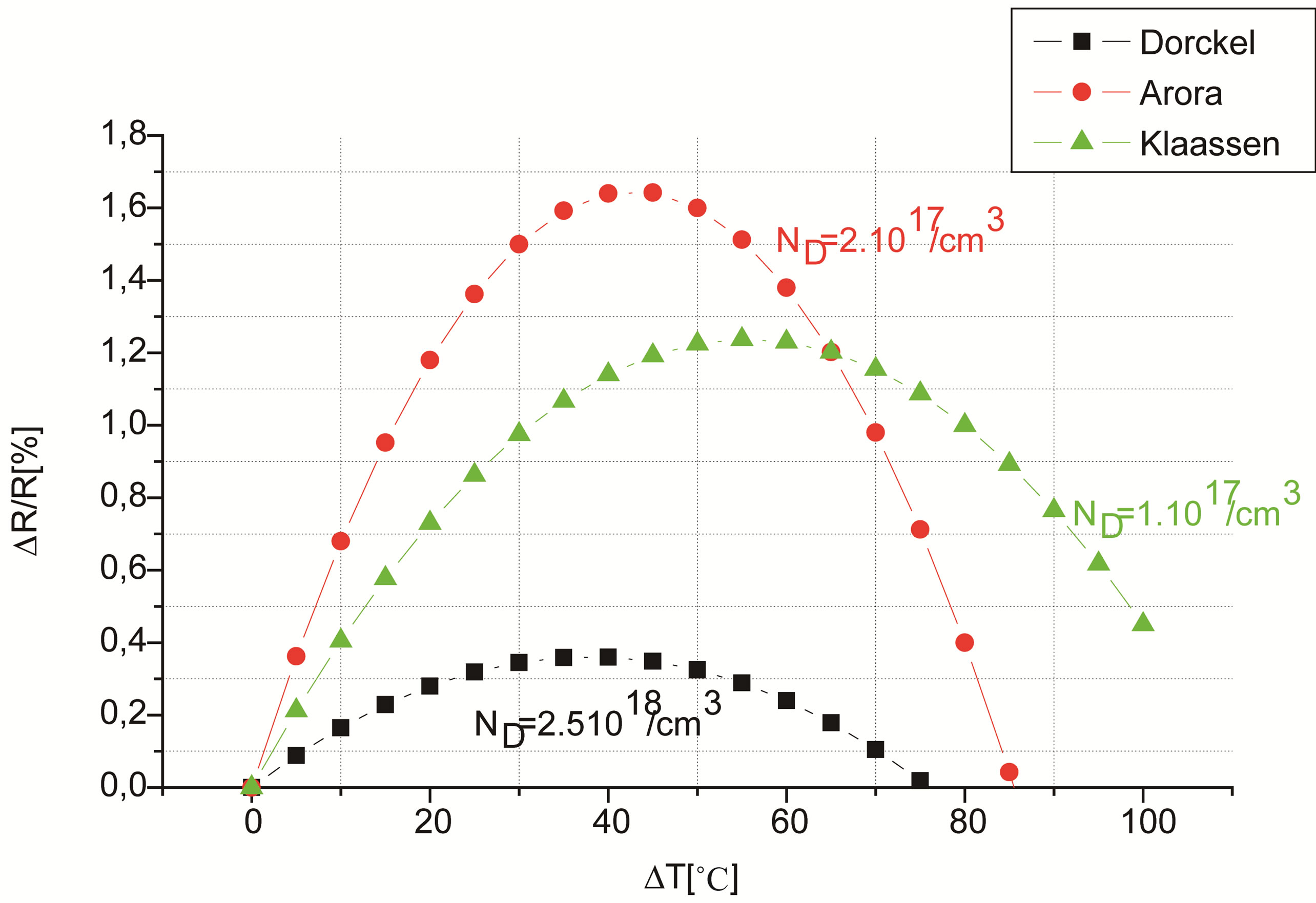
Figure 6. Variations of the relative resistance ( ) as a function of the temperature gradient ΔT for a particular couple (αmin(ND), βmin(ND)), for a given doping concentration.
centration used to obtain a minimum thermal drift depending on the desired application.
4. Conclusion
By using three models of carriers’ mobility in silicon resistance doped with donor’s atoms, we showed that the 1st and the 2nd order thermal coefficient can present a minimal value for a given doping. In addition, the comparison of the variations in a range limited of the temperature, between resistances of the two types N and P, shows that their behaviour is similar. Indeed, there is a particular couple (αmin and βmin) which allow the lineari zation of the curve  for a P-type resistor, but not for the type N. The obtained results can help the designer of more complex circuits, to choose the used resistors doping concentrations. Thereby, further enhance the performance of these devices in terms of thermal drift, according to the desired application.
REFERENCES
- A. Boukabache and P. Pons, “Doping Effects on Thermal Behaviour of Silicon Resistor,” Electronics Letters, Vol. 38, No. 7, 2002, pp. 342-343. doi:10.1049/el:20020221
- N. D. Arora and D. J. Roulston, “Electron and Hole Motilities in Silicon as a Function of Concentration and Temperature” IEEE Transactions on Electron Devices, Vol. 29, No. 2, 1982, pp. 292-295. doi:10.1109/T-ED.1982.20698
- D. B. M. Klaassen, “Unified Model for Device Simulation-I-II. Temperature Dependence of Carrier Mobility and Life Time A,” Solid State Electronic, Vol. 35, No. 7, 1992, pp. 953-967.
- J. M. Dorckel and P. H. Leturcq, “Carrier Motilities in Silicon Semi-Empirically Related to Temperature, Doping and Injection Level,” Solid State Electronic, Vol. 24, No. 9, 1981, pp. 821-825. doi:10.1016/0038-1101(81)90097-6
- C. Lombardi, S. Manzini, A. Saporito and M. Vanzi, “A Physically Based Mobility Model for Numerical Simulation of Non Planar Devices,” IEEE Transacitions Computer-Aided Design, Vol. 7, 1988, pp. 1164-1171.
- T. T. Mnatsakanov, M. E. Levinshtein, L. I. Pomortseva1 and S. N. Yurkov1, “Carrier Mobility Model for Simulation of SiC-Based Electronic Devices,” Semiconductor Science and Technology, Vol. 17, No. 9, 2002, pp. 974- 977.
Appendix
In this appendix, we describe several models of mobility’s carrier used in the literature.
1. N. D. ARORA et al. Mobility Model [2]
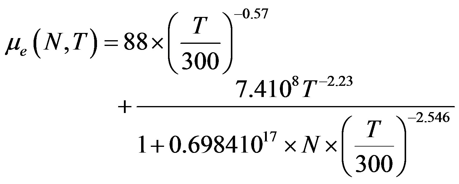 (1.1)
(1.1)
where T is the temperature in Kelvin and N is the doping concentration
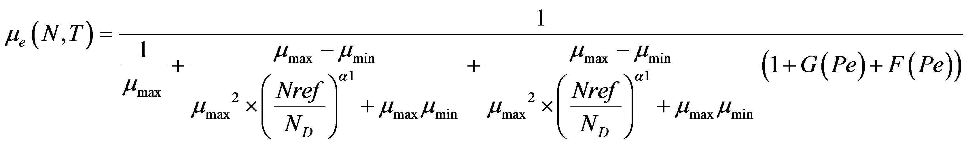
2. B. M. Klaassen Mobility Model [3]
In this model, the four contributions to the carrier mobility are taken into account, and the expression of the total mobility is:
With Pe, G (Pe) and F (Pe) are given by (2.2), (2.3) and (2.4):
 (2.1)
(2.1)
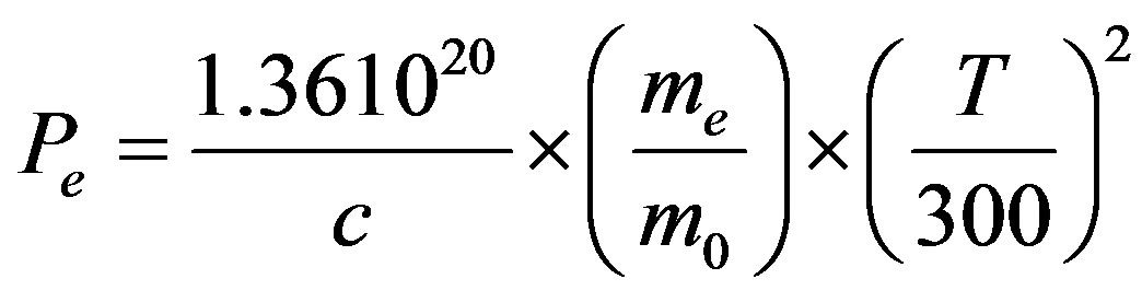 (2.2)
(2.2)
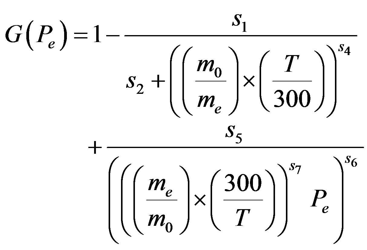 (2.3)
(2.3)
 (2.4)
(2.4)
where m and m0 are the effective and the free carrier mass respectively, T is the temperature in Kelvin, with m1 and m2 the mass of the primary and secondary scatters respectively. The model parameters for the majority electron and hole mobility given by Equation (2.1) are summarized in Table 2" target="_self"> Table 2.1. The numerical value of the constants si and ri are given in Table 2.2.
3. J. M. Dorckel et al. Mobility Model [4]
Lattice mobility µL which is connected to scattering due to acoustic phonons
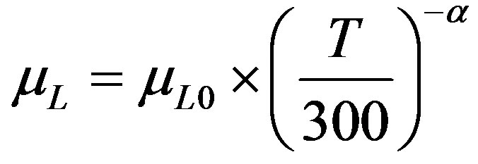 (3.1)
(3.1)
Impurity mobility µI which is connected to the interactions between the carriers and the ionized impurities
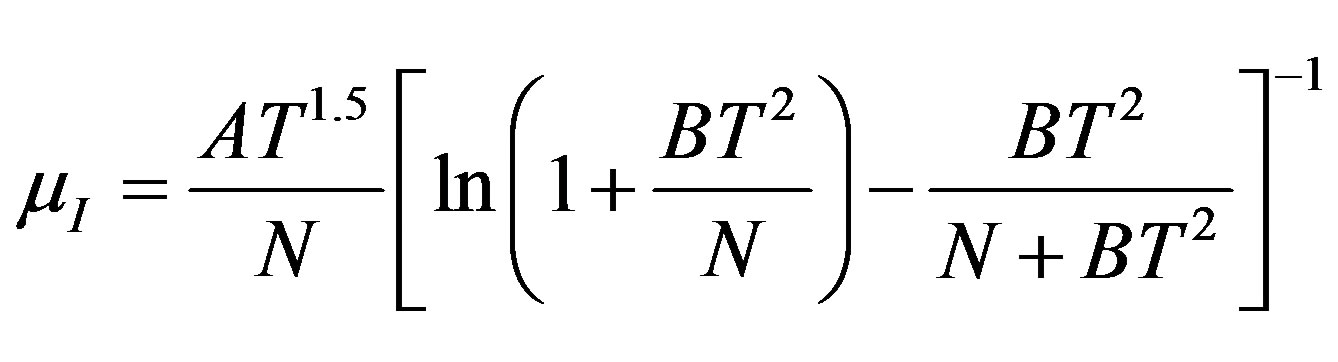 (3.2)
(3.2)
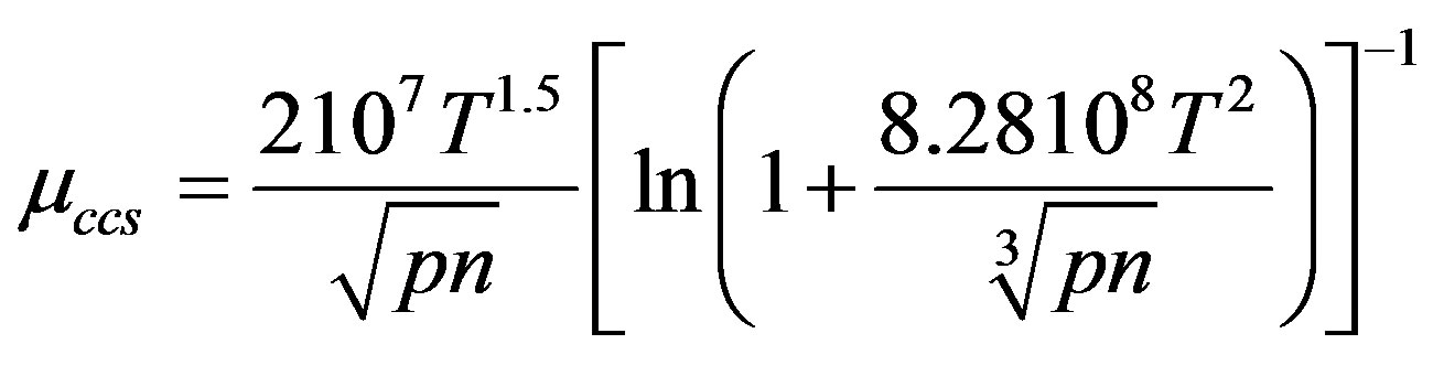
Carrier-carrier scattering mobility µccs which becomes very influential when carriers of both types are at high concentrations
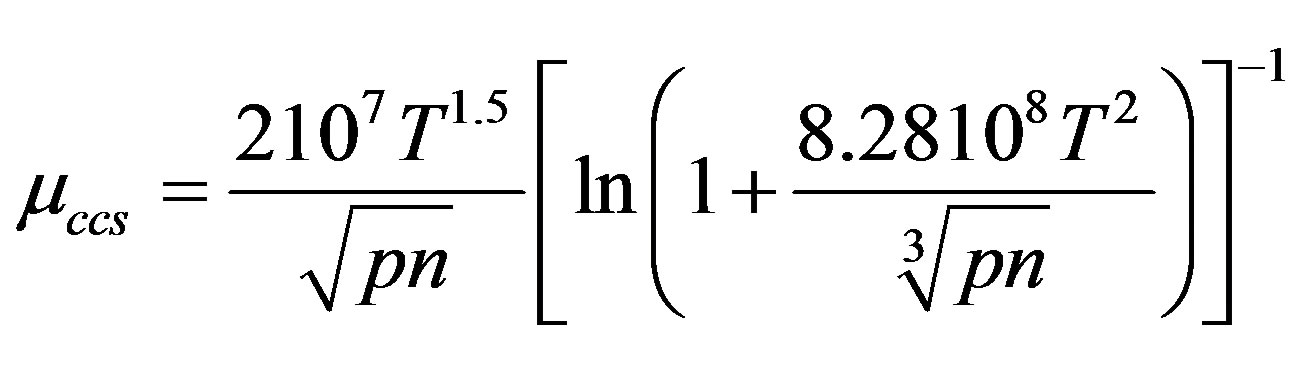 (3.3)
(3.3)
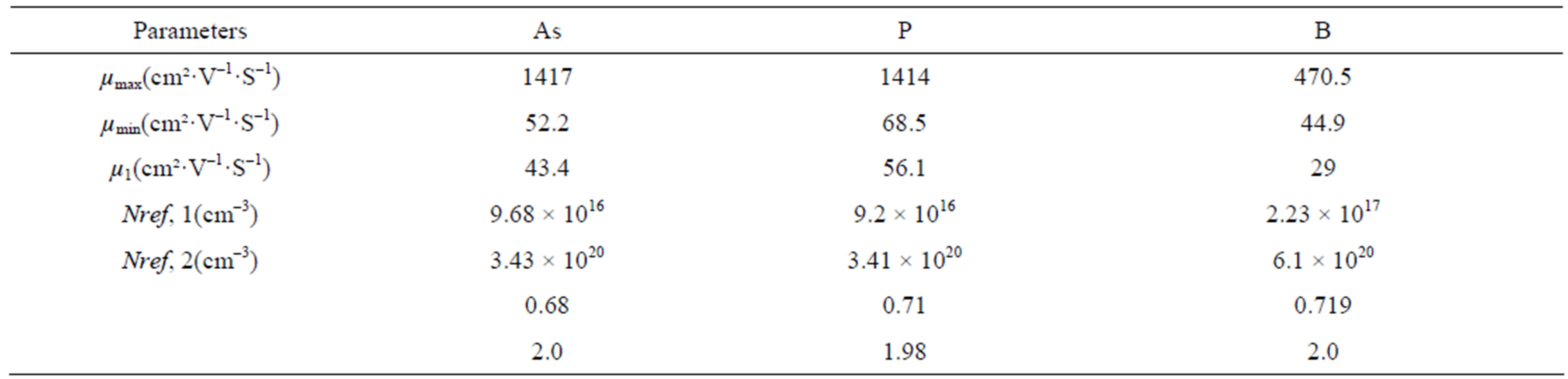
Table 2.1. Model parameters for the majority electron mobility (As and P) and majority hole mobility (B) given by Equation (2.1).
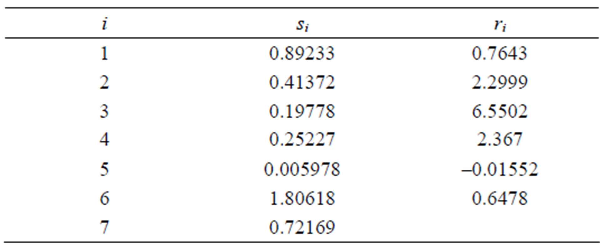
Table 2.2. Numerical values for the constants si and ri.
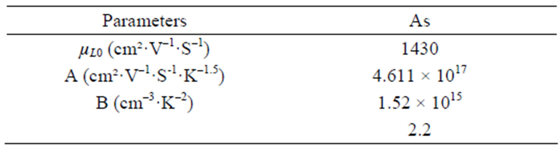
Table 3.1. Model parameters values.
 (3.3)
(3.3)
Mixed scattering mobility µIccs
 (3.4)
(3.4)
where T is the temperature in Kelvin and N is the doping concentration, µL is the lattice mobility, µI is the impurity mobility, µcss is the carrier inter-action mobility and µIcss is the carrier-impurity inter-action mobility. The model parameters values are summarized in Table 3.1.