Modeling and Numerical Simulation of Material Science
Vol.04 No.03(2014), Article ID:47928,6 pages
10.4236/mnsms.2014.43015
Numerical Simulations of Nonlinear Interaction of Space Charge Waves in Microwave and Millimeter Wave Range in n-InN Films Using Negative Differential Conductivity
Abel Garcia-Barrientos1, Volodymyr Grimalsky2
1Electronics and Computer Science Department, Research Center on Information Technology and Systems, Autonomous University of Hidalgo State (UAEH), Hidalgo, México
2CIICAp, Autonomous University of Morelos State (UAEM), Morelos, México
Email: agarciab@ieee.org
Copyright © 2014 by authors and Scientific Research Publishing Inc.
This work is licensed under the Creative Commons Attribution International License (CC BY).
http://creativecommons.org/licenses/by/4.0/


Received 14 May 2014; revised 13 June 2014; accepted 14 July 2014
ABSTRACT
Numerical simulations of nonlinear interaction of space charge waves in microwave and millime- ter wave range in n-InN films have been carried out. A micro- and millimeter-waves frequency conversion using the negative differential conductivity phenomenon is carried out when the har- monics of the input signal are generated. An increment in the amplification is observed in n-InN films at essentially at high-frequencies f < 450 GHz, when compared with n-GaAs films f < 44 GHz. This work provides a way to achieve a frequency conversion and amplification of micro- and mil- limeter-waves.
Keywords:
Space Charge Waves, InN Film, Negative Differential Conductivity

1. Introduction
Semiconducting group-III nitrides have attracted a lot of attention in the recent decade because of, mainly, the large gap (0.7 - 6.2 eV) that can be covered by the nitrides and their alloys. Their electrical and optical proper- ties are highly suitable for novel high frequency electronics, optoelectronics and photonics applications. Among those, in particular, Indium Nitride (InN) has become the focus of intense research after recent reports of an un- expectedly low band gap of 0.7 eV at room temperature [1] [2] . A great deal of experimental and theoretical ef- fort has been made to better understand the nature of InN, to determine the properties of this material, and to grow high-quality epitaxial InN layers. InN is a promising material, for colorful display, high efficiency solar cells of low cost and high-frequency electronics for its high electron mobility due to its large drift velocity at room temperature. For high-frequency electronics applications, specially, millimeter and sub-millimeter micro- wave ranges are very important for applications in communications, radar, meteorology and spectroscopy. However, the structure of semiconductor devices (transistors, diodes, etc.), required for such a short wavelength, becomes very complex, which makes its fabrication difficult and expensive with actual technologies. One potential alternative to explore the use of such a part of the electromagnetic spectrum resides in the use of non-linear wave interaction in an active media. For example, the space charge waves in thin semiconductor films, possess- ing negative differential conductivity, GaAs [3] , InP [4] , GaN [5] , and InN [6] propagate at frequencies that are higher than the frequencies of acoustic and spin waves in solids. Space charge waves have been researched since a long time ago, which can be traced back to the 1950s [7] . The early experimental work on the amplification of space charge waves with a perturbation field started in the 1970s [7] - [9] and continued today. As pointed out in 1970, in the seminal book by Scott [9] on active and nonlinear wave propagation in electronics, there was, by that time, research stretching back to the 1950s on devices such as traveling-wave tubes and backward-wave oscillators. Devices based on space charge waves use an attractive property of III-Nitride semiconductors, the nega- tive differential conductance. An electric field in excess of 50 kV/cm applied to an n-InN sample causes the dif- ferential electron mobility to become negative. To analyze wave phenomena in thin films of two-valley semiconductors [10] , a set of equations to describe the charge transport is commonly used. In this theory, with small initial perturbations, continuity, momentum and energy equations, and Poisson’s equation are solved numerical- ly. The solutions show that the modulations of electron density travel along the beam in the form of waves called space charge waves. Although, this paper presents the numerical simulations of amplification and propa- gation of space charge waves in InN films, the experimental verification can be carried out in the same way like in GaAs films, already reported in Ref. [11] .
2. Electron Transport Model
Nonlinear interaction of space charge waves in microwave and millimeter wave range in n-InN films using the negative differential conductivity will be one of the most relevant topics in microelectronics and communica- tions in the coming years, due to the potential it represents in terms of amplification of micro- and millimeter- waves. Therefore, we present two-dimensional numerical simulations of propagation and amplification of space charge waves in InN films and microwave frequency conversion under negative differential conductivity phe- nomenon. We use a high quality, single crystal wurtzita InN film placed onto substrate without a acoustic con- tact. It is assumed that the electron gas is localized in the center of film. The thickness of the n-InN film is 2 h ≤ 1 μm, see Figure 1.
The coordinate system is chosen as follows: X-axis is directed perpendicularly to the film, the electric field E0

Figure 1. The structure of the n-InN traveling-wave amplifier with an epitaxial layer.
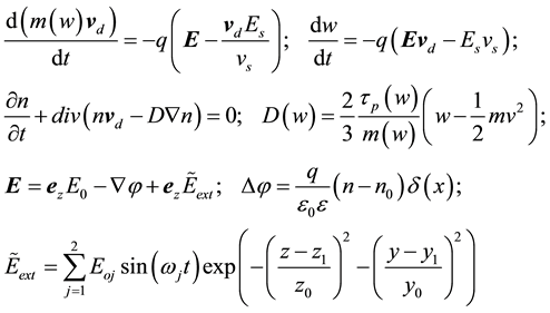
is applied along Z-axis, exciting and receiving antennas are parallel to Y-axis. 2D model of electron gas in the n-InN film is used. Taking a constant surface sheet density of 2D n0 = 2.5 × 1013 cm−2 for a 1 µm thick film. There has been some evidence to suggest the presence of electron accumulation at the surface of InN, including measurements of the sheet carrier density as a function of InN film thickness and capacitance-voltage profiling [12] . The space charge waves possessing phase velocity equal to drift velocity of the electrons v0 = v(E0), E0 = U0/Lz, are considered, where U0 is bias voltage, Lz is the length of the film. Generally, a non-local dependence of drift velocity vd of electrons on the electric field takes place. In simulations, an approximation of two-dimen- sional electron gas is used. The set of balance equations for concentration, drift velocity, and the averaged energy to describe the dynamics of space charge waves within the n-InN film takes a form, like in GaAs film [10] :
 (1)
(1)
where vd is drift velocity, φ is the of potential, n = n0 + ñ where n0 is constant electron concentration, ñ is the varying part, w is the electron energy, D is the diffusion coefficient, and ε0 is the lattice dielectric permittivity of n-InN, m(w) is averaged effective mass, q is the electron charge, τp,w(w) are relaxation times, Eext is a small mi- crowave electric signal applied to the input antenna and E0 is the bias electric field. It is assumed that a condition of occurring negative differential conductivity is realized. Because the signal frequencies are in microwave or millimeter wave range, it is possible to separate diffusion and drift motions. For the sake of simplicity, instead of relaxation times, the parameter Es is introduced [10] :
 (2)
(2)
In such a representation, the mean energy and mean effective mass of electron are denoted by w and m(w), the equilibrium value of w is w0; A direct correspondence between local field dependence and non-local effects is well seen. Because a dependence Es = Es(w) is unique, it is possible to express the parameters w and vs through the value of Es. The dependencies of drift velocity, averaged electron energy, and effective mass versus electric field in InN films were calculated by our Monte Carlo procedure, which are pretty similar as experimental re- sults [13] - [15] . Several stochastic mechanisms such as acoustic phonon, polar optical phonon, inter-valley pho- non, Coulomb, and piezoelectric scattering are considered and their impact is assessed. The parameter values for the acoustic deformation potential (ADP Ξ = 7.1 eV), polar-optical phonon scattering (ħω = 73 meV or 89 meV), inter-valley scattering (ħωiv = ħωLO), mass density (ρ = 6.81 g/cm3), and static and high frequency dielectric constants (εs = 15.3 and ε∞ = 8.4) are adopted from [16] . In addition, we study the influence of another set of di- electric constants (εs = 11.0 and ε∞ = 6.7) recently proposed in [16] in conjunction with the narrow bandgap and lower effective mass. The dependencies of drift velocity, averaged electron energy and averaged electron mass on electric field in InN films are taken from our Monte Carlo simulation results (see Figure 2), which are in good agreement with measured data and the set of parameters used in the simulations are very similar from lite- rature [13] -[16] . The maximum value of drift velocity in InN is when the electric field is ~40 kV/cm, under these high-field conditions, some of the electrons can acquire enough energy from the electric field to transfer via inter-valley scattering to the upper valley. Since the mobility of electrons in the upper valley is smaller than in lower valley, the conductivity decreases with increasing field, leading to a negative differential resistance (see Figure 2(a)). A comparison of the results for GaAs and InN films reveals that for the field strength considered most of the electrons in GaAs are in higher valley while in InN less than are transferred. This is due to the dif- ference in the separation of the valleys (0.3 eV in GaAs and ~ 2.9 - 3.9 eV in InN [17] ) in spite of the higher
 (a)
(a)
 (b) (c)
Figure 2. Electron drift velocity (a), average electron energy (b), averaged mass (c) versus electric field used in simulations.
field applied in InN. A large negative differential conductance appears when increasing electric field more than the threshold fielded; the electrons have not enough energy to make the inter-valley scattering. Beyond this val- ue, the optical scattering mechanisms play a drastic role rather than acoustic and ionized impurity scattering.
Since this process is inelastic, the electron energy curves have sensitive variation in its slope; in fact it does not increase as fast as increasing in initial fields (see Figure 2(b)).
3. Propagation and Amplification of Space Charge Waves in n-InN Films
The spatial increment of space charge waves is investigated by the dispersion equation, D(ω,k) = 0, the relation between angular frequency, ω = 2πf, and wave vectors, consider these like complex,  , where
 . The dispersion relation is obtained using balance equations model, set Equations (1), with some transformation we can obtain Equation (3),
 (3)
(3)
but if we assume that ñ obeys the law ~exp(iωt-ikz), Equation (3) gives the dispersion relation:
 (4)
(4)
In general, we consider the cases where ω = 2πf is real and  has real and imaginary part. The case
  corresponds to spatial increment (amplification), whereas the case
  corresponds to the decre- ment (damping). In Figure 3(a), the spatial increment of space charge waves in an n-InN film is shown in the curve 3, where the electron concentration is n0 = 2.5 × 1013 cm−2, the bias electric field is E0 = 50 kV/cm. In curve 2, the electron concentration is n0 = 2 × 1013 cm−2 with the same bias electric field, E0 = 50 kV/cm. Curve 1 is the result for n-InN films where the electron concentration is n0 = 2.5 × 1013 cm−2 and the bias electric field is E0 = 45 kV/cm. The stationary values of E0 have been chosen in the regime of negative differential conductivity (dv/dE < 0) for all cases. One can see that an amplification of space charge waves in InN films occurs in a

 (a) (b)
Figure 3. (a) The spatial increment of space charge waves in an n-InN film is shown in the curve 3, where the electron con- centration is n0 = 2.5 × 1013 cm−2, the bias electric field is E0 = 50 kV/cm. In curve 2, the electron concentration is n0 = 2 × 1013 cm−2 with the same bias electric field, E0 = 50 kV/cm. Curve 1 is the result for n-InN films where the electron concen- tration is n0 = 2.5 × 1013 cm−2 and the bias electric field is E0 = 45 kV/cm; (b) Spectral components of the electric field of space charge waves. The effective excitation of harmonics is presented. The input carrier frequency is f = 60 GHz.
wide frequency range, and the maximal spatial increment is k'' = 12 × 105 m−1 at the frequency f = 225 GHz. When compared with a case of the GaAs film [3] , it is possible to observe an amplification of space charge waves in InN films at essentially higher frequencies f > 44 GHz. To obtain an amplification of 25 dB, it is ne- cessary to use a distance between the input and output antennas of about 19 µm.
When a small microwave electric signal  is ap-
plied to the input antenna. Here z1 and y1 are the position of the input antenna; z0 and y0 are its half-width. When this signal is applied, the excitation of space charge waves in 2D electron gas takes place. These waves are sub- ject to amplification, due to negative differential conductivity.
The set of Equations (1) form a set of non-linear coupled time dependent partial differential equations. These differential equations are discretized using a finite-difference scheme and are solved numerically. A transverse inhomogeneity of the structure in the plane of the film along Y axis is taken into account. The following para- meters have been chosen: 2D electron concentration in the film is n0 = 2.5 × 1013 cm−2, the initial uniform drift velocity of electrons is v0 ≈ 4 × 107 cm/s (E0 = 50 - 100 kV/cm), the length of the film is Lz = 5 - 20 µm, the thickness of the film is 2 h = 0.1 - 1 μm. The typical output spectrum of the electromagnetic signal is given in Figure 3(b). The input carrier frequency is f = 60 GHz. The amplitude of the input electric microwave signal is Em = 25V/cm. Although the growth rate decreases as the rf frequency increases, for our case an amplification of 25 dB is obtained. One can see both the amplified signal at the first harmonic of the input signal and the har- monic generations of the input signal, which is generated due to the non-linearity of space charge waves.
The propagation and amplification of space charge waves in n-GaAs thin films with negative difference con- ductance have been studied in the last decade [12] , however n-InN films have not been addressed yet, and are subject of this work. We address the device presented in Figure 1 by means of numerical simulations. An n-InN epitaxial film of thickness 0.1 - 1 μm is put on an InN semi-insulating substrate. The two-dimensional electron density in the film is chosen to be n0 = 2.5 × 1013 cm−2. On the film surface are the cathode and anode ohmic- contacts (OCs), together with the input and output coupling elements (CEs). The CEs connect the sample struc- ture to microwave sources. A dc bias voltage (above the Gunn threshold, 50 kV/cm) was applied between the cathode and anode OCs, causing negative differential conductivity in the film. The CEs perform the conversion between electromagnetic waves and space charge waves, where the excitation of space charge waves in the 2D electron gas takes place.
The spatial distributions of the alternate component of the electric field E~z and E~y are shown in Figure 4. One can see the maximum variations are in the output antenna. The length of the film is 20 µm. The transverse width of the film along Y axis is 40 µm. The duration of the input electric pulse is 2.5 ns. The spatial distribu- tions are presented for the time moment 1.5 ns after the maximal value of the input signal. Direct numerical si-

 (a) (b)
Figure 4. The spatial distributions of the alternative part of the electric field component E~z (a) and E~y (b) of space charge wave; The length of the film is 20 µm. The transverse width of the film along Y axis is 40 µm.
mulations have confirmed pointed below results on linear increments of space charge waves amplification. Also a possibility of non-linear frequency doubling and mixing is demonstrated. To get the effective frequency doubl- ing in the millimeter wave range, it is better to use the films with uniform doping.
4. Conclusion
A numerical simulation of nonlinear interaction, two-dimensional propagation and amplification of space charge waves in microwave and millimeter wave range in n-InN films using negative differential conductivity are pre- sented. A microwave frequency conversion using the negative differential conductivity phenomenon is carried out when the harmonics of the input signal are generated. A comparison of the calculated spatial increment of instability of space charge waves in n-GaAs and n-InN films is performed. An increment in the amplification is observed in n-InN films at essentially higher frequencies f > 44 GHz than in GaAs films [3] . The maximum am- plification (gain of 25 dB) is obtained at f = 225 GHz, using a distance between the input and output antennas of about 19 µm.
Acknowledgements
This project has been funded by the CONACyT-Mexico grant CB-169062 and also it has been partially funded by PROMEP: Redes Temáticas de Colaboración under the project titled: Fuentes de Energías Alternas.
References
- Wu, J., Walukiewicz, W., Shan, W., Yu, K.M., Ager III, J.W., Haller, E.E., Lu, H. and Schaff, W.J. (2002) Effects of the Narrow Band Gap on the Properties of InN. Physical Review B, 66, Article ID: 201403. http://dx.doi.org/10.1103/PhysRevB.66.201403
- Wu, J., Walukiewicz, W., Yu, K.M., Ager III, J.W., Haller, E.E., Lu, H., Schaff, W.J., Saito, Y. and Nanishi, Y. (2002) Unusual Properties of the Fundamental Band Gap of InN. Applied Physics Letters, 80, 3967-3969.
- Garcia, A., Grimalsky, V., Gutierrez, E. and Palankovski, V. (2009) Nonstationary Effects of the Space Charge in Se- miconductor Structures. Journal of Applied Physics, 105, Article ID: 074501. http://dx.doi.org/10.1063/1.3093689
- Garcia-Barrientos, A. and Palankovski, V. (2011) Numerical Simulations of Space Charge Waves in InP Films and Microwave Frequency Conversion under Negative Differential Conductivity. Applied Physics Letters, 98, 072110-1- 072110-3.
- Koshevaya, S.V., Grimalsky, V.V., Garcia-B, A. and Diaz-A, F. (2012) Amplification and Nonlinear Interaction of Space Charge Waves of Microwave Band in Heterogeneous Gallium Nitride Films. Radioelectronics and Communica- tions Systems, 55, 289-298. http://dx.doi.org/10.3103/S0735272712070011
- Schley, P., Goldhahn, R., Gobsch, G., Feneberg, M., Thonke, K., Wang, X. and Yoshikawa, A. (2009) Influence of Strain on the Band Gap Energy of Wurtzite InN. Physica Status Solidi (b), 246, 1177-1180. http://dx.doi.org/10.1002/pssb.200880924
- Beck, A.H.W. (1958) Space-Charge Waves and Slow Electromagnetic Waves. Pergamon, New York.
- Dean, R.H., Dreeben, A.B., Kaminski, J.F. and Triano, A. (1970) Travelling-Wave Amplifier Using Thin Epitaxial GaAs Layer. Electronics Letters, 6, 775-776.
- Scott, A. (1970) Active and Nonlinear Wave Propagation in Electronics. John Wiley & Sons, New York.
- Carnez, B., Cappy, A., Kaszynskii, A., Constant, E. and Salmer, G. (1980) Modeling of a Submicrometer Gate Field- Effect Transistor Including Effects of Nonstationary Electron Dynamics. Journal of Applied Physics, 51, 784-790. http://dx.doi.org/10.1063/1.327292
- Mikhailov, A.I. (2000) Experimental Study of the Parametric Interaction between Space-Charge Waves in Thin-Film GaAs-Based Semiconductor Structures. Technical Physics Letters, 26, 217-219. http://dx.doi.org/10.1134/1.1262796
- Lu, H., Schaff, W.J., Eastman, L.F. and Stutz, C.E. (2003) Surface Charge Accumulation of InN Films Grown by Mo- lecular-Beam Epitaxy. Applied Physics Letters, 82, 1736. http://dx.doi.org/10.1063/1.1562340
- Tansley, T. and Foley, C. (1984) Electron Mobility in Indium Nitride. Electronics Letters, 20, 1066-1068. http://dx.doi.org/10.1049/el:19840729
- Yamamoto, A., Shin-ya, T., Sugiura, T. and Hashimoto, A. (1998) Electron Mobility in Indium Nitride. Journal of Crystal Growth, 189/190, 461-465. http://dx.doi.org/10.1016/S0022-0248(98)00331-5
- Franssen, G., Suski, T., Perlin, P., Teisseyre, H., Khachapuridze, A., Dmowski, L.H., Plesiewicz, J.A., Kaminska, A., Kurouchi, M., Nanishi, Y., Lu, H. and Schaff, W. (2006) Band-to-Band Character of Photoluminescence from InN and In-Rich InGaN Revealed by Hydrostatic Pressure Studies. Applied Physics Letters, 89, Article ID: 121915. http://dx.doi.org/10.1063/1.2356994
- Polyakov, V. and Schwierz, F. (2006) Low-Field Electron Mobility in Wurtzite InN. Applied Physics Letters, 88, 032101-1-032101-3. http://dx.doi.org/10.1063/1.2166195
- Bougrov, V., Levinshtein, M.E., Rumyantsev, S.L. and Zubrilov, A. (2001) Properties of Advanced Semiconductor Materials GaN, AlN, InN, BN, SiC, SiGe. In: Levinshtein, M.E., Rumyantsev, S.L. and Shur M.S., Eds., John Wiley & Sons, Inc., New York, 1-30.