Natural Resources
Vol.4 No.1A(2013), Article ID:29421,4 pages DOI:10.4236/nr.2013.41A018
Copper Zinc Sulfur Compound Solar Cells Fabricated by Spray Pyrolysis Deposition for Solar Cells
![]()
1Department of Electric Engineering and Computer Sciences, University of Hyogo, Hyogo, Japan; 2Energy Technology Laboratories, Osaka Gas Co., Ltd., Osaka, Japan.
Email: *itou@eng.u-hyogo.ac.jp
Received January 16th, 2013; revised February 17th, 2013; accepted February 26th, 2013
Keywords: Cu2Zn2S3; Spray Pyrolysis; Solar Cells; Superstrate Structure; TiO2
ABSTRACT
Cu-Zn-S (CZS) films were deposited by the spray pyrolysis method. As-deposited CZS film showed a low crystallinity. The resistivity of CZS film with  ratio of 50% is around
 . The CZS film elements using spray
  solution with thiourea was confirmed as
  by ICP-MS and EDX. The band gap of CZS films was varied in the range of 1.8 - 3.5 ev when the
  ratio was increased from 0% to 67%; CZS film with
  ratio of 50% showed an wide band gap of 2 eV. The photovoltaic characteristics were confirmed with cell structure of
 . The best cell was observed at the CZS films with
 ratio of 50%; these cells depicted a conversion efficiency of 1.7%.
1. Introduction
Compound solar cells as Cu(InGa)Se2 (CIGS), CuInS(or Se)2 (CIS) solar cells have shown high durable and high efficiency (Record efficiency 20.3%) [1]. These solar cells have been normally fabricated by vacuum method. The vacuum process has the high cost of equipment and low process speed for production. In addition, the CIS and CIGS solar cells use expensive materials as gallium and indium. Therefore, Cu-Zn-Sn-S(Se) compound (CZTSSe) which does not use indium has been developed recently (the record efficiency 10.1%) [2]. The advantage of CZTSSe solar cells is using non-vacuum method and without expensive materials. However, CZTS solar cell using four or five elements including Cu, Zn, Sn, S, and Se, is so complex. For this reason, we have tried to develop Cu-Zn-S compound (CZS) with three elements for absorber layer in solar cells; this compound can be simpler in comparison with CZTS. Some groups reported about this material for applications in Inorganic Electro-Luminescence [3,4] or just basic research as semiconductor [5-7]. In our work, the CZS films were prepared by spray pyrolysis method, which is non-vacuum and low cost. This is the first report of CZS for applications in solar cells.
In this paper, we fabricated CZS films with different  ratios. Optical, electrical and photovoltaic properties were analyzed in detail. Conversion efficiency of 1.72% was obtained at CZS solar cells with
  structure.
2. Experimental
The CZS layers were prepared on glass substrates by spray pyrolysis. The spray solution included 150 mM of  and 60 ml of Cu-Zn source
  . The
. The  ratios varied in the range of 0% - 67%. The solution (30 ml) was sprayed onto the substrates at temperature of 277˚C in air ambience. The formation of the CZS crystal was confirmed by X-ray diffraction (XRD; Miniflex 2, Rigaku using CuKα radiation) measurement. The shapes and elemental ratio of CZS crystals were measured using a TEM-EXD system (JEM2100F, JEOL Co. Ltd.). The composition of CZS film was also measure by inductively coupled plasma-mass spectroscopy (ICP-MS). The resistivity of CZS films was calculated from sheet resistance four-probe measurement. The carrier concentration and mobility were obtained by Hall-effect measurement (ResTest8300, Toyo Technica Co. Ltd.). The absorption spectra of CZS films were measured by ultraviolet-visible spectroscopy (Lambda 750 UV/VIS, Perkin-Elmer). The distribution of elements including Cu, Zn, In, S and Ti in the cell cross-section was confirmed by an electron probe micro-analyzer (EPMA). Photovoltaic measurements employed an AM 1.5 solar simulator equipped with a xenon lamp (YSS-100A, Yamashita Denso, Japan). The power of the simulated light was calibrated to 100 mW·cm−2 by using Si solar cell reference. CZS solar cells with structure of
  were fabricated. 300 nm-In2S3 buffer layer and 500 nm-TiO2 compact layers were also fabricated by spray pyrolysis method. Carbon paste was printed on cells as back electrode. Cells were scratched except just under back electrode. Figure 1 shows the samples before and after scratching.
3. Results and Discussions
The composition of the sprayed CZS films measured by Inductively Coupled Plasma (ICP) and TEM-EDX is Cu3.9Zn3.8S5.9 and Cu28.65Zn27.37S43.95, respectively; these elemental results are concluded to , which corresponds to the ion number of Cu+ and Zn2+. In spite of the deposition under ambient atmosphere, Cu was become Cu+, but not oxidized to Cu2+. This is due to the effect of thiourea.
Figure 2(a) shows a TEM image of spray-pyrolysis CZS. It can be observed that some parts of CZS were crystalized to ca. 10 nm particles. The electron diffraction pattern (Figure 2(b)) shows the Debye-Scherrer ring, which suggests that the spray-pyrolysis CZS is the aggregate of nanoparticles. For the comparison, a TEM image of CZS by ball-milling synthesis is shown (Figure 2(c)). The ball-milling CZS particles were ca. 100 nm, and the particle was close to a single crystal, judged from the diffraction pattern (Figure 2(d)).
Figure 3 shows the variation of the resistivity of CZS films with different  ratios. The resistivity of CZS films is rather low. The resistivity was increased with decreasing Cu concentration from 67% to 18.7%. Below 18.7%, we cannot measure the resistivity because of the high resistance of CZS films.
By the Hall-effect measurement using a CZS film with , the CZS was a p-type semiconductor, and the carrier concentration and mobility was 3.06 × 1021 cm−3 and
 , respectively

Figure 1. Solar cell structures before and after scratching the CZS layer.
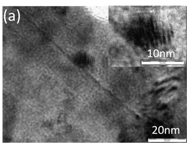
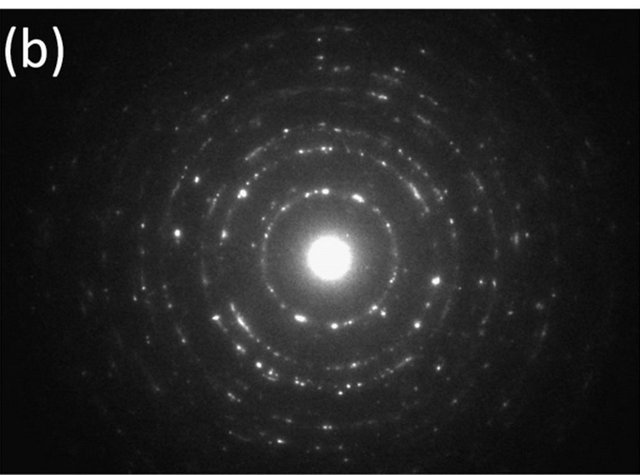
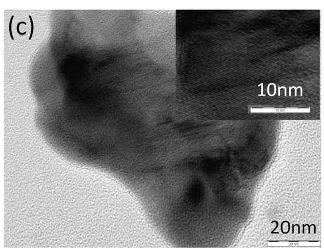
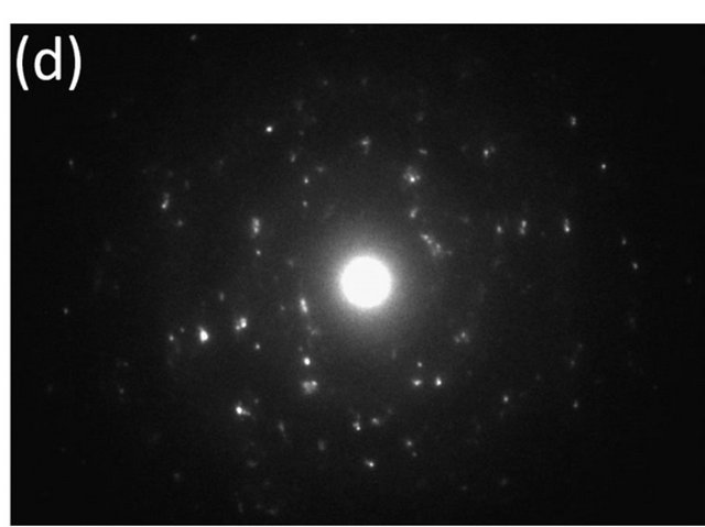
Figure 2. A TEM image (a) and an electron diffraction pattern (b) of CSZ by spray pyrolysis deposition, and a TEM image (c) and an electron diffraction pattern (d) of CSZ by ball-milling synthesis.
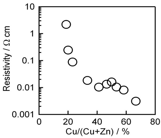
Figure 3. Resistivity of CZS films with different  ratios.
The carrier concentration was quite high as a p-type semiconductor, which may due to the surface defect on the CZS nano crystal.
Figure 4(a) shows a plot of absorption coefficient as a function of photon energy  for the CZS film with different
 ratios. The band gap of CZS films was shifted towards low energy with increasing Cu concentration. The variation of CZS band gap value with
  ratio was shown in Figure 4(b). The band gap value varied in the range from 1.8 eV to 3.6 eV with the variation of
  ratios from 67% to 0%. The results indicate that CZS is wide band gap materials.
Figure 5 shows EPMA results on cross-section of the  films. The result showed that copper diffused into In2S3 layer, but zinc did not diffuse into In2S3 layer. It was speculated that a thin layer of CuInS2 may be formed at the interface between CZS and In2S3; CuInS2 and In2S3 can make p-n junction and the cells can generate electricity [8]. However, typical CuInS2 peaks
 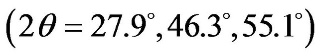 were not observed from the results as shown in Figure 6. Since the CuInS2 layer is too thin, the XRD system could not detect the CuInS2 peaks.
The photocurrent-voltage of CZS cells with and without scratching was shown in Figure 7(a). The CZS layer of this cell was prepared with  ratio of 50%. After scratching, the photocurrent became lower than the sample without scratching. Figure 7(b) shows photocurrent-voltage of CuInS2 (CIS) spray cells with and without scratching for comparison. After scratching, the photocurrent did not change in the CIS solar cell with the sample without scratching the CIS layer. Therefore,
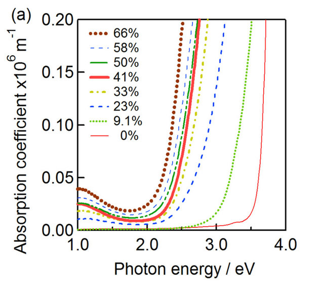
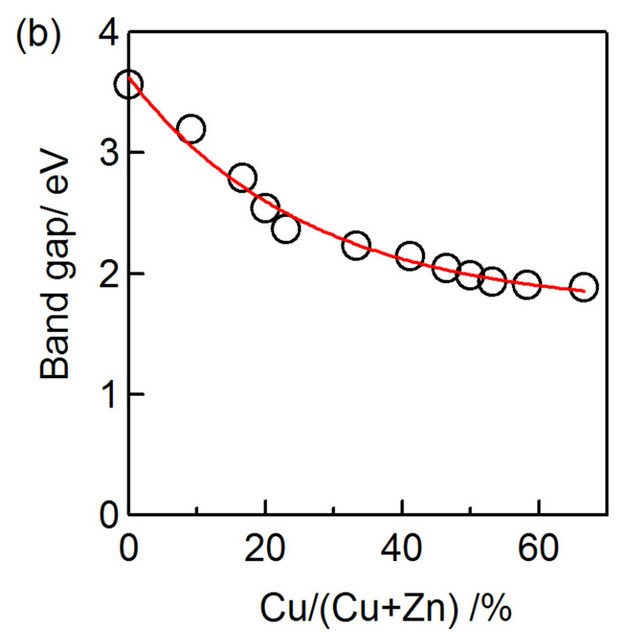
Figure 4. CZS absorption spectra (a) and the band gap variation (b) of CZS with different  ratios.
 (a)
(a)
Figure 5. Electron probe micro analysis (EPMA) spectra (a) and the elemental mapping images (b) of  on cross-section at
  .
.
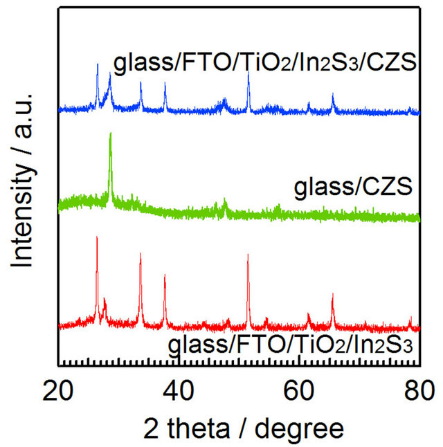
Figure 6. X-ray diffraction patterns of  ,
,  and
and  .
.
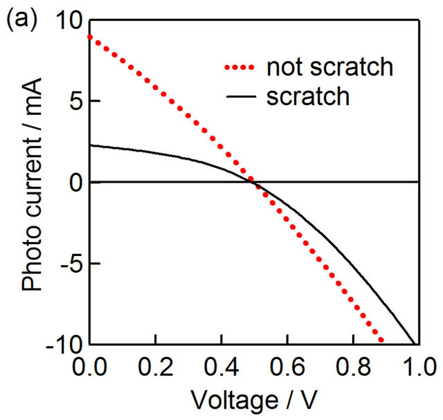
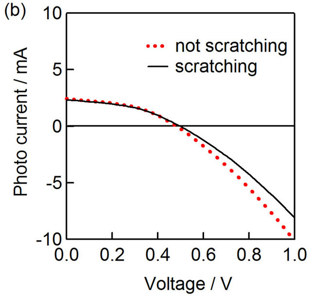

Figure 7. Photovoltaic characteristics of CIS and CZS solar cells with/without scratching. I-V curves of  CZS (a) and CuInS2 (b) solar cells with and without scratching. The schemes of electron flow in CZS (c) and CIS (d) solar cells.
the difference of CZS photocurrent was due to the high conductivity of CZS films, which can collect the generated holes effectively from the surrounding (Figure 7(c)). On the other hand, the conductivity of CuInS2 layer was lower (ca. 0.1 Ω−1·cm−1), and the hole were able to be transferred from the CuInS2 layer just under the back electrode (Figure 7(d)).
Figure 8 shows the variation of conversion efficiency of CZS solar cells with  ratios. The conversion efficiencies, which were lower than 0.5% in the range below 33% and over 67% of
  ratio, performed over 1% from 42% to 58% of
  ratio. The cells at 50% ratio of
  showed the peak of photoenergy conversion efficiencies.
Figure 9 shows the current density-voltage curves of the best cell with  ratio of 50%. The shortcircuit photocurrent (Jsc), open-circuit photovoltage (Voc), fill factor and conversion efficiencies were 9.12 mA·cm−2, 0.492 V, 0.383 and 1.72%, respectively. It was noticed

Figure 8. The variation of photoenergy conversion efficiencies of CZS solar cells with different  ratios.

Figure 9. Current density-voltage curves of a best cell with  under light (AM1.5, 100 mW·cm-2) and dark conditions. The cell area was
  .
.
that the dark and light curves indicate crossing point at 0.53V. This crossing point suggests double diode interfaces in a solar cell [9].
4. Conclusion
CZS films were deposited by spray pyrolysis at 277˚C in air ambience. The resistivity of CZS films increases with decreasing copper concentration. The band gap of CZS films varied in the range from 1.8 to 3.5 when  ratio changed in the range from 67 % to 0%. A strong diffusion of Cu atom from CZS layer into In2S3 layer was observed. The diffusion of Cu atom from CZS into In2S3 may form a thin CIS layer between CZS and In2S3. The best efficiency of 1.27% was obtained at CZS cells with
  ratio of 50%.
5. Acknowledgements
A part of this work was supported by NEDO (Japan).
REFERENCES
- P. Jackson, D. Hariskos, E. Lotter, S. Paetel, R. Wuerz, R. Menner, W. Wischmann and M. Powalla, “New World Record Efficiency for Cu(In,Ga)Se2 Thin-Film Solar Cells beyond 20%,” Progress in Photovoltaics: Research and Applications, Vol. 19, No. 7, 2011, pp. 894-897. doi:10.1002/pip.1078
- D. Aaron, R. Barkhouse, O. Gunawan, T. Gokmen, T. K. Todorov and D. B. Mitzi, “Device Characteristics of a 10.1% Hydrazine-Processed Cu2ZnSn(Se,S)4 Solar Cell Photovoltaic,” Progress in Photovoltaics: Research and Applications, Vol. 20, No. 1, 2012, pp. 6-10.
- J. Huang, Y. Yang, S. Xue, B. Yang, S. Liu and J. Shen, “Photoluminescence and Electroluminescence of ZnS:Cu Nanocryttals in Polymeric Networks,” Applied Physics Letters, Vol. 70, No. 18, 1997, pp. 2335-2337. doi:10.1063/1.118866
- W. Q. Peng, G. W. Cong, S. C. Qu and Z. G. Wang, “Synthesis and Photoluminescence of ZnS:Cu Nanoparticles,” Optical Materials, Vol. 29, No. 2-3, 2006, pp. 313- 317. doi:10.1016/j.optmat.2005.10.003
- M. A. Yildirim, A. Ateş and A. Astam, “Annealing and Light Effect on Structural, Optical Properties of CuS, CuZnS and ZnS Thin Films Grown by the SILAR Method,” Physica E, Vol. 41, No. 8, 2009, pp. 1365-1372. doi:10.1016/j.physe.2009.04.014
- C. C. Uhuegbu, E. B. Babatunde and C. O. Oluwafemi, “The Study of Copper Zinc Sulphide (CuZnS2) Thin Films,” Turkish Journal of Physics, Vol. 32, No. 1, 2008 pp. 39-47.
- C. C. Uhuegbu and E. B. Babatunde, “Spectral Analysis of Copper Zinc Sulphide Ternary Thin Film Grown by Solution Growth Technique,” American Journal of Scientific and Industrial Research, Vol. 1, No. 3, 2010, pp. 397-400. doi:10.5251/ajsir.2010.1.3.397.400
- T. Ryo, D.-C. Nguyen, M. Nakagiri, N. Toyoda, H. Matsuyoshi and S. Ito, “Characterization of Superstrate Type CuInS2 Solar Cells Deposited by Spray Pyrolysis Method,” Thin Solid Films, Vol. 519, No. 21, 2011, pp. 7184-7188. doi:10.1016/j.tsf.2010.12.176
- J. Gao, J. M. Luther, O. E. Semonin, R. J. Ellingson, A. J. Nozik and M. C. Beard, “Quantum Dot Size Dependent J-V Characteristics in Heterojunction ZnO/PbS Quantum Dot Solar Cells,” Nano Letters, Vol. 11, No. 3, 2011, pp. 1002-1008. doi:10.1021/nl103814g
NOTES
*Corresponding author.