Optics and Photonics Journal
Vol.3 No.4(2013), Article ID:35630,4 pages DOI:10.4236/opj.2013.34046
Opto-Electronic Investigation of Wet Coating Deposition of ITO Nanopowders on Flexible Substrate Using Pulse Nd-YAG Laser
1Faculty of Chemical Technology, Iranian Research Organization for Science and Technology, Tehran, I. R. Iran
2Department of Chemistry, AmirKabir University of Technology, Teheran, I. R. Iran
Email: *Salar@irost.org
Copyright © 2013 H. Salar-Amoli, H. Amani. This is an open access article distributed under the Creative Commons Attribution License, which permits unrestricted use, distribution, and reproduction in any medium, provided the original work is properly cited.
Received May 23, 2013; revised June 26, 2013; accepted July 15, 2013
Keywords: Pulse Nd-YAG Laser; PET; Spin Coating; Flexible Substrate; Opto-Electronic
ABSTRACT
Transparent thin layer indium tin oxide was coated on polyethylene tetraphetalate (PET) substrate by means of spin coating process and its opto-electronic properties have been investigated. The surface treated by pulse Nd-YAG laser. Pulse frequency, duration and energy were, 1000 Hz, 0.2 to 20 ms and 25 to 40 J respectively. The effect of treatment on crystallization, optical properties and bonding processes of the thin layer was investigated. The results show that ITO coated on flexible PET substrates is conductive and transparent. The sheet transparency for a 350 nm thickness in the visible range is more than 83.6%. Using Nd-YAG laser increased conductivity by a factor of 100 times and causes higher bonding performances.
1. Introduction
Due to special properties of indium tin oxide (ITO) and ITO doped materials, it is widely used for many applications [1,2]. ITO also has singular optical and electrical properties in crystal serving flat display, thin film transistor and solar cells. However, most of researcher was using glass substrates to deposit the films [3,4], while few reports treated the polymer substrate [5,6].
Nowadays, there is a demand for production of flexible conductive polymer, and this area is a popular research zone which could affect on technology development, especially in the field of touch-panel display and solar cell industries [7,8]. The main problem which still remains is the annealing of the substrate. Since polymers cannot tolerate the high temperature, it is not possible to use high temperature as annealing mode for crystallization.
In this work PET has been used as substrate due to its low density and softness. PET also has been used widely in the electrical industries due to its dielectric and mechanical properties and there is a suitable adhesion between the ITO and flexible PET.
Using bonding materials is a major technique for bonding the ITO on polymer substrate. In this process a monomer can be treated by heat or UV light to form a polymer with a good bonding strength between the two layers. But this adhesive method suffering from contamination and lowering conductivity [9]. Recently bonding energy is used instead of bonding materials [10,11], in this processes energy from sources such as Nd-YAG laser is applied on the contacting boundary to melt and fuse the layers. Both continuous and pulsed laser is used for the wide range of materials includes dielectric to metal ceramics, semi conductors, polymer and biological tissue [12].
This paper reports on the latest achievements of ITO coating by spin process and pulse Nd-YAG laser treatment techniques.
2. Experimental
The principle of operation is based on our previous work [13,14]. Indium tin oxide nanopowders can be fully dispersed in alcohol by applying ultrasonic energy. The ITO sols were deposited on PET substrates by a spin coating process which was made in our lab. The optimum spin rate was found to be 1100 rpm for 30 seconds. The resulting sheets were first cured at 180˚C up to 60 min before treatment with laser.
A pulse Nd-YAG laser, model 1QL-10 was used as the laser source. Pulse frequency was between 1000 to 1500 Hz, duration was between 0.2 to 20 ms and the applied energy was between 25 to 40 J. The bonding and crystallization process by the laser source carried out either in single or replicated steps.
The resistance, measured by a multimeter model “Sanwa-JP-120” and transmittance of thin film coated on PET substrate measured in the spectra range of 300 to 800 nm with a UV-VIS “Perkin Elmer Spectrometer”. The surface morphologies were characterized by optical microscope mode, ZEISS-Axisokop 2 MAT and scanning electron microscope (SEM) “ZEISS DSM-960 A”.
3. Results and Discussions
PET has excellent flexibility, reliability and light weight, so it is a good candidate for substrate of devices including organic electronic, biomedical and flexible display. The substrates should be clean and without any impurity and dusts and before layer deposition should be treated carefully. Otherwise poor performance of untreated substrate causes low conductivity and no adhesion effect [15, 16].
In this work 5 × 5 cm sheet of PET was treated by distilled water, weak acids and bases and spin coating process has been used as a high speed processing, low device cost and ability to coat from a very thin (few hundred nanometer) to thick (few micrometer) homogeny layer. Prior to spin coating, Sonication of the ITO liquid has been used for breaking intermolecular interaction and dispersing nanoparticles in liquid to obtain smooth films with high optical transmittance.
The main challenge of using flexible substrate is limitation of temperature treatment [7] to value up to 180˚C. Annealing of the substrate was carried out by heating at maximum tolerable temperature and the resistance obtained was above 500 KΩ. In these conditions the ITO cannot be crystallized completely. This value remains constant as long as the sheet is kept in vacuum or in protective atmosphere. But when laser used as a step for crystallization and bonding treatment, a significant improvement achieved. Figure 1 shows the effect of pulse Nd-YAG laser on resistance with or without annealing at 180˚C. At optimum point, when the thickness of ITO layer on PET substrate increased to 350 - 400 nm, the resistance reduced dramatically to about 0.6 KΩ.
Figure 2 shows the SEM morphologies for ITO films deposited on PET substrate. ITO films grown on PET substrate showed very smooth surface morphology. Excellent flexibility of the transparent ITO coated sheet is shown in Figure 3. Further experiment has been done to

Figure 1. Resistance of inorganic ITO layer as a function of films thicknesses. (A) Laser treatment (B) Heating at 180˚C + Laser treatment.
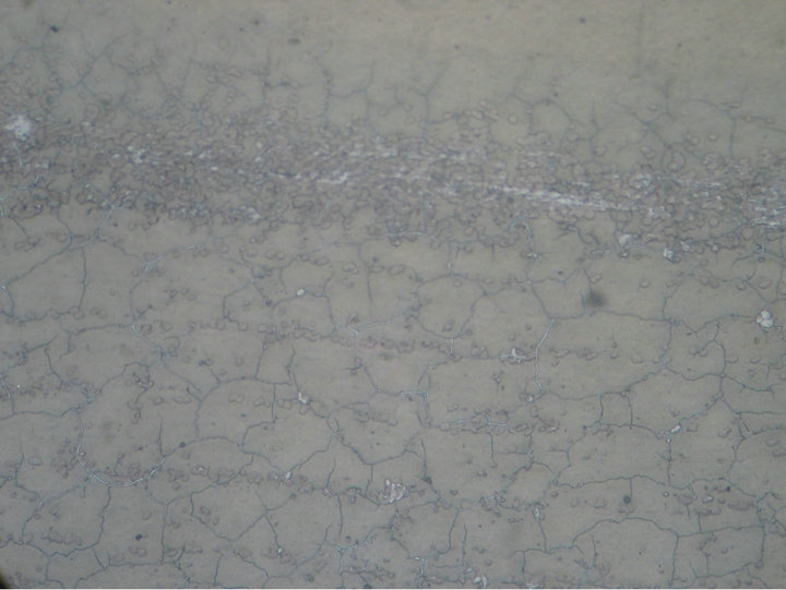
Figure 2. SEM morphology for inorganic ITO films deposited on PET substrate.
reduce the resistance by doping the ITO layer. Metal particles such as silver were added to ITO sols to make them more conductive. In practice, while this will render the coating electrically more conductive, it will also make them opaque with very low transparency. As results no significant changes for improving quality of the coated substrate obtained.
ITO main feature is the combination of two main factors which are conductivity and transparency. It has been reported that the thickness of ITO thin film directly affect on both these factors [11,12]. When the thickness of ITO layer increased, the conductivity of the sheet increased as well, but its transparency decreases, so a compromise has to be reached during film deposition. In this work thickness of thin layers controlled by the spinning rate per minute and the concentration of the ITO solution. In final a 350 - 400 nm thickness has been selected for further experiment.
Atomic force microscopy images of ITO deposited on PET at thickness of 200 to 400 nm is shown in Figure 4. The roughness value Ra is about 0.96 nm with a peak to valley maximum value of PV = 12.5 nm.
Figure 5 shows that the optical transmittance in the UV-VIS region of ITO films changes with different thicknesses and strong correlation with electrical resistivity. The optical transmittance obtained is greater than 83% in the visible range. As thickness increases the PET resistivity and optical transmittance decreases.

Figure 3. A photo of conductive, transparent and flexible PET.


Figure 4. Atomic force microscopy images of the surface of a 200 to 300 nm thick ITO/PET cured by Nd-YAG pulse laser.
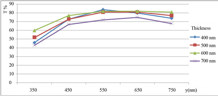
Figure 5. Optical transmittance as a function of the light wavelength and ITO thicknesses deposited on PET substrate.
4. Conclusion
A simple and economic method is used to prepare transparent and conductive polymer. Indium thin oxide films were deposited on flexible PET substrate by spin coating process and its opto-electronic properties have been investigated. Treatment of the sheet by pulse Nd-YAG laser at 25 to 40J energy shows crystallization of ITO with conductivity of less than 0.6 kΩ and transparency of 83.6%. This study shows a great achievement toward production of flexible conductive films.
REFERENCES
- W. Zhu, G. Wang, X. Hong, X. Shen, D. Li and X. Xie, “Metal Nanoparticle Chains Embedded in TIO2 Nanotubes Prepared by One-Step Electrodeposition,” Electrochimica Acta, Vol. 55, No. 2, 2009, pp. 480-484. doi:10.1016/j.electacta.2009.08.059
- B. ORegan and M. Gratzel,” A Low Cost High Efficiency Solar Cell Based on Dye Sensitized Colloidal TIO2 Films,” Nature, Vol. 353, No. 6346, 1991, pp. 737-740. doi:10.1038/353737a0
- H. C. Lee and O. Oak-Park “The Evolution of the Structural Electrical and Optical Properties in Indium-Tin Oxide Thin Film on Glass Substrate by DC Reactive Magnetron Sputtering,” Vacuum, Vol. 80, 2006, pp. 880-887. doi:10.1016/j.vacuum.2005.11.069
- S.-J. Hong and J.-I. Han “Indium Tin Oxide Thin Film Fabricated by Indium-Tin-Organic Sol including ITO Nanoparticle,” Current Applied Physics, Vol. 6, Suppl. 1, 2008, pp. 206-210. doi:10.1016/j.cap.2006.01.041
- L. G. Li, G. H. Lu, X. N. Yang and E. L. Zhou, “Progress in Polymer Solar Cell,” Chinese Science Bulletin, Vol. 52, No. 2, 2007, pp. 145-158. doi:10.1007/s11434-007-0001-y
- M. A. Green, “Thin-Film Solar Cells: Review of Materials, Technologies and Commercial Status,” Journal of Materials Science: Materials in Electronics, Vol. 18, No. 1, 2007, pp. S15-S19. doi:10.1007/s10854-007-9177-9
- W. J. Lee, E. Ramasamy, D. Y. Lee and J. S. Song, “Glass Frit Overcoated Silver Grid Lines for Nanocrysyalline Dye Sensitized Solar Cells,” Journal of Photochemistry and Photobiology A: Chemistry, Vol. 183, No. 1-2, 2006, pp. 133-137. doi:10.1016/j.jphotochem.2006.03.006
- S. I. Na, B. K. Yu, S. S. Kim, D. Vak, T. S. Kim, J. S. Yeo and D. Y. Kim, “Fully Spray-Coated ITO Free Organic Solar Cells for Low Cost Power Generation,” Solar Energy Materials & Solar Cells, Vol. 94, No. 8, 2010, pp. 1333-1337. doi:10.1016/j.solmat.2010.01.003
- E. Shigeno, K. Shimizu, S. Seki, M. Ogawa, A. Shida, M. Ide and Y. Sawada, “Formation of Indium Tin Oxide Films by Dip Coating Process Using Indium Dipropionate Monohydroxide,” Thin Solid Films, Vol. 411, No. 1, 2002, pp. 56-59. doi:10.1016/S0040-6090(02)00187-6
- G. H. A. Therese and P. V. kamath, “Electrochemical Synthesis of Metal Oxides and Hydroxides,” Chemistry of Materials, Vol. 12, No. 5, 2000, pp. 1195-1204. doi:10.1021/cm990447a
- S. Zh. Karazhanov, “Temperature and Doping Level Dependence of Solar Cell Performance including Excitons,” Solar Energy Materials& Solar Cells, Vol. 63, No. 2, 2000, pp. 149-163. doi:10.1016/S0927-0248(99)00173-7
- M. Hidalgo, F. Martin and J. J. Laserna, “Laser-Induced Breakdown Spectrometry of Titanium Dioxide Antireflection Coatings in Photovoltaic Cells,” Analytical Chemistry, Vol. 68, 1996, pp. 1095-1100. doi:10.1021/ac951002i
- H. Salar Amoli and B. Fathi, “Effect of Pulse Nd-YAG Laser Beam Interaction on Annealing of Nanopowder ITO Using Spin-On-Glass” Journal of Sol-Gel Science and Technology, Vol. 59, No. 1, 2011, pp. 32-35. doi:10.1007/s10971-011-2457-0
- H. Salar Amoli, S. Shokatian and M. Abdous, “Thermal Annealing Combination with Pulse Nd-YAG Laser Treatment of ITO on Polycarbonate Using Spin Coating Process,” Journal of Sol-Gel Science and Technology, Vol. 62, No. 3, 2012, pp. 319-323. doi:10.1007/s10971-012-2727-5
- S. Maridha and D. Basak, “Effect of Thickness on the Structural, Electrical and Optical Properties of ZNO Films,” Materials Research Bulletin, Vol. 42, No. 5, 2007, pp. 875-882. doi:10.1016/j.materresbull.2006.08.019
- W. J. Lee, E. Ramasamy and D. Y. Lee, “Effect of Electrode Geometry on the Photovoltaic Performance of Dye-Sensitized Solar Cells,” Solar Energy Materials & Solar Cells, Vol. 93, No. 8, 2009, pp. 1448-1451. doi:10.1016/j.solmat.2009.03.002
NOTES
*Corresponding author.