Engineering
Vol. 2 No. 11 (2010) , Article ID: 3167 , 4 pages DOI:10.4236/eng.2010.211111
An Explicit Surface-Potential Based Biaxial Strained-Si n-MOSFET Model for Circuit Simulation
Department of Electronics and Electrical Communication Engineering, Indian Institute of Technology, Kharagpur, India
E-mail: tkm.iitkgp@yahoo.com
Received May 23, 2010; revised September 28, 2010; accepted November 3, 2010
Keywords: Strained-Si, Heterostructure, 2-DEG, Surface Potential, Regional Approach
ABSTRACT
In this paper, a charge sheet surface potential based model for strained-Si nMOSFETs is presented and validated with numerical simulation. The model considers sub band splitting in the 2-DEG at the top heterointerface in SiGe layer and also the dependence of electron concentration at heterointerface with the gate oxide. The model is scalable with strained-Si material parameters with physically derived flat-band voltages. An explicit relation for surface potential as a function of terminal voltages is developed. The model is derived from regional charge-based approach, where regional solutions are physically derived. The model gives an accurate description of drain current both in the weak and strong inversion regions of operation. The results obtained from the model developed are benchmarked with commercial numerical device simulator and is found to be in excellent agreement.
1. Introduction
As conventional Si MOSFETs are scaled into nanometer regime, maintaining performance enhan-cement beyond 90-nm technology node is becoming extremely difficult. Stress/strain engineering has now become indispensable to meet the performance targets of the International Technology Roadmap for Semiconductors (ITRS) for devices [1]. According to the ITRS roadmap, a precisely controlled process flow for the incorporation of new material such as, strained-Si in Si CMOS technology is becoming crucial for deep sub-micron CMOS devices.
Among the possible solutions, engineered substrates, in particular, substrate-induced strained silicon (strained-Si) has been identified as very promising for channel engineered MOSFETs as it improves the CMOS performance [2-6]. In this case, the strain is introduced at the substrate level before the transistor is built (opposite to process-induced strain currently being used in 45 nm technology node).
Due to strain introduction at the starting materials stage, global or wafer-scale strained-Si is more universal in nature and some of its attributes or specifications can be addressed more generally. The approach depends largely on materials engineering, rather than device design. The strain stretches the silicon lattice by about 1%. For strained-Si, a graded layer of silicon germanium (SiGe) is grown on top of a bulk silicon wafer. A typically 2 μm thick SiGe layer having a 20-30% germanium concentration, with a higher concentration of germanium atoms at the top is used. Then a relatively thin layer of silicon, about 20-nm thick, is deposited on top of the SiGe layer. For detail, the reader may refer to the special issue on strained-Si: materials and devices [7]. The technology for the growth of high quality strained-Si layer on completely relaxed, step-graded, SiGe buffer layer has been reviewed by Maiti et al. [8-10].
Since early 1990s, strained-Si on silicon germanium (SiGe) substrates is being explored in an effort to boost CMOS performance [8,11,12]. The mobility advantage the strain offers at no significant additional processing cost which makes it an important candidate among various choices for performance enhanced devices. Until now, the substrate-induced biaxial strain has offered the best results for long channel (over 100% mobility enhancement) which, however, indeed occurs at low electric field and for high strain.
For biaxial tensile strain, the key component of the enhanced mobility results from the lowest energy subband having a low conductivity effective mass. Biaxial tension in strained-Si grown on relaxed-Si1 – xGex virtual substrates alters the Si band structure by splitting the subband degeneracy in both the conduction and valence bands and reducing the band gap [13,14].
2. Strained-Si CMOS Technology
Towards strained-Si CMOS technology development, low temperature oxidation and the deposition of other dielectric film formation such as nitride, oxynitride on strained-Si have been reviewed in reference [15]. However, many issues remain unresolved. Currently, research in this area is mainly focused on its use for low power digital circuit design. However, as with all CMOS generations, there will eventually be strong interest in mixed-signal applications. The efficiency in the design of both the digital and analog integrated circuits depends very much on the accuracy of the analytical transistor models involved in the circuit simulation. In particular analog circuit simulation requires an accurate prediction of drain current as a function of the applied voltage.
Compact MOSFET models can be broadly classified into three categories, i.e. 1) threshold voltage based models, 2) inversion charge based models and 3) surface potential based models. The earliest MOSFET model included in the SPICE circuit simulator was threshold voltage based. However, inherent discontinuities in capacitances and conductances across different operating regions limit the use of this model [16]. Complexity is also an important constraint for the so-called compact transistor models; the model used should be as simple as possible in order to limit circuit simulation time. Moreover, it has been found that it fails to predict correctly the harmonics of intermodulation distortion in RF circuits [17]. Several compact models for bulk-Si MOSFETs have been developed and are in use for efficient IC design. Surface potential and inversion charge based compact models have been developed to avoid above problems [18-21].
The surface potential based model (SPBM) for the bulk MOSFET has now been widely accepted as the de-facto industry standard as it is able to predict the output characteristics accurately. But the problem with SPBMs is that an implicit equation has to be solved [22] to evaluate the correct surface potential (SP) in all regions of operation. However, the solution of these equations iteratively, using numerical algorithms [23], results in computational inefficiency and non-convergence in circuit simulators. In order to reduce computation time, an explicit, yet accurate, relation between surface potential Φs and the terminal voltages is preferable.
Several analytical models for threshold voltage have been reported in the literature [24-27]. However, to the best of our knowledge, there is no surface potential based analytical model of drain current for strained-Si n-MOSFETs considering the sub band splitting in the two-dimensional electron gas (2-DEG). Such models would be necessary in order to incorporate these devices in the next generation CMOS VLSI circuit design.
In this paper, we report on the surface potential based analytical model for drain current of heterostructure strained-Si n-MOSFETs considering the carrier transport at the strained-Si/SiGe heterointerface as well as at strained-Si/SiO2 interface. The physics-based model includes a regional approximated expression for weak and strong inversion and is scalable with the terminal bias and also strained-Si material parameters, such as, Ge mole fraction (x), strained-Si layer thickness (tSSi) and wide doping range (NSSi) considered in the investigation. The key idea is to derive physical relations of the flat-band voltages (VFB) for the strained-Si devices and apply them to the regional surface-potential (Φs) and charge-based solutions that can be added to form a unified solution. In this work, our main focus has been in the weak to strong inversion region and to derive relations which are suited for circuit simulation. In Section 3, the analytical model for the current-voltage (I-V) characteristics for strained-Si n-MOSFETs has been developed. The results are compared with numerical simulated data in Section 4.
3. Analytical Model
3.1. Device Structure and Operation of Strained-Si n-MOSFETs
A schematic diagram of a strained-Si n-MOSFET is shown in Figure 1, where VG, Vds, and Vbs represent the gate, drain, and bulk voltages, respectively. It may be noted that for the n-MOSFET, VG and Vds are positive voltages while Vbs is usually negative. The device consists of a SiO2 gate dielectric layer of thickness tox, and strained-Si layer of thickness tStSi, and a relaxed SiGe buffer layer of thickness tSiGe. These layers are grown on a p-type substrate.
Other important parameter for strained-Si MOSFETs
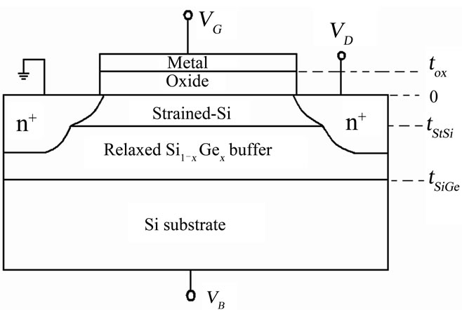
Figure 1. Cross-sectional view of a strained-Si n-MOSFET.
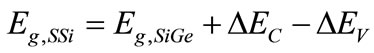
is the Ge mole fraction (x) in Si1−xGex, which not only determines the conduction-band discon-tinuity (∆EC ) at the Si/Si1 – xGex heterointerface but also the mobility of electrons in the 2-DEG. The typical values of these parameters are tox = 10 nm, tSSi = 20 nm, x = 0.20, and NSSi = 1 × 1017 cm−3. The depletion-layer width (W) in the doped silicon substrate extended as VG is made more positive and reached a maximum value at VG = VTSiGe, when strong inversion occurs at the top heterointerface (x = tStSi). With further increase in VG, the sheet electron concentration in the 2-DEG in SiGe at the StSi/SiGe heterointerface will increase, resulting in an increased potential drop across the strained silicon and oxide layers. Figure 2 shows the energy band diagram of the metal/SiO2/strained-Si/SiGe/p-Si structure under this condition. At VG = VTSSi, the bands bend sufficiently to create inversion at the Si/SiO2 interface. When VG > VTSSi, the drain-current (Ids) is due to the flow of electrons in the strained-Si/SiGe heterojunction as well as the StSi/SiO2 interface. For analytical modeling of the drain current of strained-Si/SiGe n-MOSFETs, it is necessary to obtain suitable expressions for the electron concentrations in both the channels as a function of VG. This is discussed in the next two sub-sections.
3.2. Position of Fermi Level in Strained-Si Layer
The lattice mismatch between Si and Ge, which is 4.2% at room temperature, requires tensile or compressive strain of the active Si1 – xGex layer to match the in-plane lattice when it is pseudomorphically grown on a Si1 – yGey substrate layer (x ≠ y) [2]. Strain changes the band structure and form band offset between the active material and the substrate material. This paper focused on the biaxial tensile strained-Si on relaxed SiGe heterostructure. Biaxial strain is composed of uniaxial extension in growth direction and a hydrostatic strain in all directions
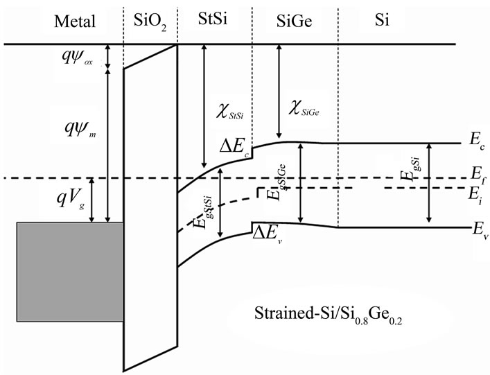
Figure 2. Energy band diagram of metal/SiO2/SSi/SiGe/p-Si structure.
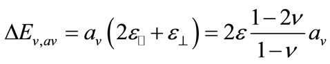
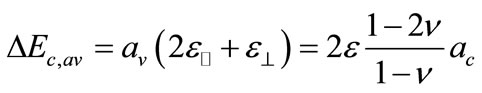
[2]. The uniaxial components give rise to splitting of degenerate energy levels, whereas the hydrostatic component give rise to uniform shift of the center of gravity [8]. Hydrostatic strain shifts the average position of the valence and the conduction band by  and
and , respectively [8],
 (1)
(1)
 (2)
(2)
where ν is Poisson’s ratio. av and ac are the numerical values of the hydrostatic deformation potentials.  and
and  represents parallel (in-plane) and perpendicular (to the interface) strain tensor.
  represents the strain state of the semiconductor. For simplicity we assume the perpendicular direction in [001], a threefold degenerate valence band at k = 0 (light holes 1, heavy holes 2, spin-orbit split-off holes 3) and an indirect conduction band with sixfold degenerate Δ valleys (in the (100) directions). The biaxial strain in the epitaxial plane can be considered as hydrostatic deformation superposed by an uniaxial strain
 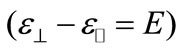 perpendicular to the plane. In the absence of strain the threefold degeneracy of the valence band is already lifted by the spin orbit interaction and splits the bands by an amount of Δ0. With respect to the average band position Ev,av two bands are shifted up by an amount of
  (the light and heavy hole bands, which are denoted Ev1, Ev2), while one band is shifted down by an amount
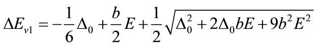
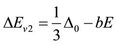
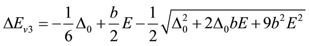
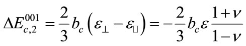
  (the spin-orbit split-off band, which we denote Ev3). For completeness the relations of band offset, lifting of the valence band degeneracy by strain and spin-orbit interaction have been considered. The superposition of both effects is nonlinear for the light hole and spin orbit split-off band. The energy splitting of the valance bands is given by [8,28],
 (3)
(3)
 (4)
(4)
 (5)
(5)
Under the action of uniaxial strain along [001] direction, the bands along [100] and [010] directions split off from the one along the [001] direction, i.e. it lifts the sixfold degeneracy of the conduction band into the fourfold degenerate bands with energy minima lying in-plane and the twofold degenerate band with energy minima lying perpendicular to the (001) plane. The uniaxial induced energy shifts of the conduction bands are given by [28]
 (6)
(6)
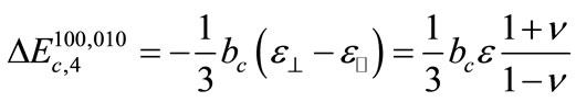 (7)
(7)
For av = 2 eV, ac = 3 eV, bv = –2.5 eV, bc = 9 eV, Δ0 = 0, ν = 1/3 under either tensile biaxial strain of magnitude 0.01 the band average Ev,av is shifted up by 20 meV. Tensile strain further shifts up the light hole (l h) energy levels by 100 meV while heavy holes (hh) are lowered by 50 meV and the spin-orbit split-off holes (soh) are degenerate (Δ0 = 0) with heavy holes at k = 0. As a result of tensile strain the light holes energy (Ev1) are lifted by 120 meV, while the heavy holes (Ev2 = Ev3) are lowered by 30 meV.
The conduction band splitting (ΔEc,splitting) between the lower m-fold degenerate bands and the raised n-fold degenerate bands may be determined from Equations (6) and (7); where for tensile strain, m = 2 and n = 4 and in the case of compressive strain, m = 4 and n = 2. The effective density of states in the conduction band, Nc,SSi is therefore defined by [29,30]:
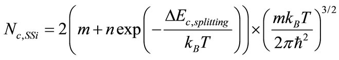 (8)
(8)
where kB is the Boltzman constant, m is effective mass of electron. In the valance band, strain causes the splitting of degenerate valance bands at the Γ point. The splitting reduces the occupation in the lowered subvalleys and therefore decreases the density of states. The valance band splitting (ΔEv,splitting) can be obtained from Equations (3), (4) and (5). Thus Nv,SSi can be obtained using an analysis analogous for Nc,SSi [29,30]:
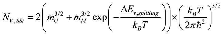 (9)
(9)
where mU and mM are the effective hole masses of the raised and lower band respectively. The contribution of spin split-off band (v3) have been neglected because it is far from the top of the valance band edge. The band gap and affinity can be expressed as:
 (10)
(10)
 (11)
(11)
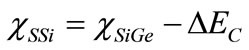
where the indexes ‘SSi’ corresponds to the bandgap and affinity values for strained-Si. is the electron affinity of the SiGe. Since, we are concerned with the strained-Si channel, valance and conduction band off-set are calculated with respect to strained-Si layer. Ge mole fraction dependent expressions are given by [31,32]:
 (12)
(12)
 (13)
(13)
 (14)
(14)
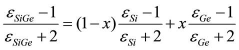
where Eg,SiGe, NC,SiGe, and NV,SiGe are the band gap, conduction and valence band densities of states in SiGe, respectively. To estimate the permittivity of the Si1 – xGex alloy, we use the Clausius-Mossotty relationship [33]:
 (15)
(15)
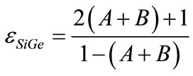
Based on the above relation, the following simplified expression may be obtained as:
 (16)
(16)
where 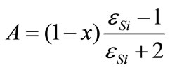 and
and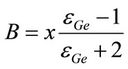 .
.
The above models are incorporated in the Sentaurus device [34] simulator (for comparison study) as well as in our analytical model. The intrinsic carrier density of strained-Si and SiGe layer may be expressed as,
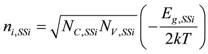 (17)
(17)
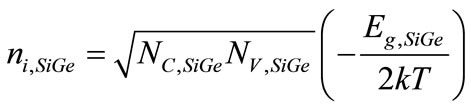 (18)
(18)
where NC,SSi and NV,SSi are the conduction and valence band densities of states in strained-Si, respectively. Now an average Fermi potential in for strained-Si can be expressed as:
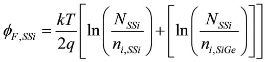 (19)
(19)
3.3. Sheet Electron Concentrations in Channels as Functions of VG
For strained-Si MOSFETs, the bandgap, affinity, density of states, and intrinsic carrier density of the strained-Si and SiGe layers are function of stress and Ge mole fraction in the Si1 – xGex layer. An accurate determination of the voltages at which electron accumulation at different interfaces occurs is the key to the physical modeling of the charges in strained-Si MOSFETs. Here we use subscripts “1” and “2” to denote physical quantities at the strained-Si/SiO2 and strained-Si/SiGe interfaces, respectively. The strained-Si flat band (ignoring depletion within a thin layer of Debye length) is defined as the voltage at which the accumulation starts at the strained-Si/SiO2 interface and is given by,
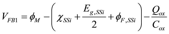 (20)
(20)
Hole accumulation at the strained-Si/SiGe interface occurs when VGB reaches the flat band voltage VFB2, at which the top strained-Si layer is depleted of mobile charges. At VGB = VFB2, a thin layer equivalent to the Debye length is also depleted. VFB2 can be calculated from the Poisson’s solution as
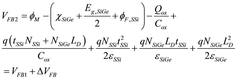 (21)
(21)
where 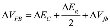 (22)
(22)
and 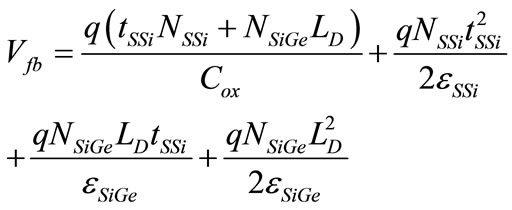 (23)
(23)
is the flat band shift due to the charges and potential drops in the strained-Si and the Debye length in SiGe is, given by
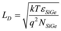 (24)
(24)
The depletion region should lie between VFB2 and Vt, since below VFB2, holes start to accumulate at the strained-Si/SiGe interface.
3.4. Drain-Current Model
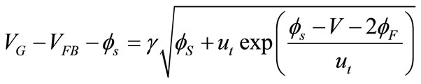
The Pao-Sah relation [35] for surface potential based bulk Si MOSFET is given by,
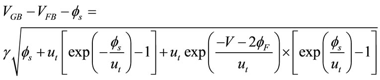 (25)
(25)
where VFB is the flatband voltage, ut is the thermal voltage defined by kT/q,  is the strained-Si Fermi potential defined by Equation (19) and γ is the body factor defined by
 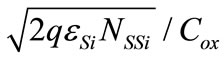 and the gate oxide capacitance per unit area Cox is given by εox/tox. The bulk referenced quasi-Fermi potential V is equal to Vbs and Vbd at the source and drain end, respectively. The above relation is valid for all values of gate-bulk voltage VGB and gives an accurate description in all regions of operation (accumulation, depletion and inversion). In the useful range of operation (depletion and inversion region),
  is positive and generally
  ut. So, the Pao-Sah relation reduces to
 (26)
(26)
In the weak-threshold region (VFB1 < VG < Vt) or (0 <  < 2
< 2 + V), the exponential term in Equation (26) becomes negligible and we get a quadratic equation for surface potential. They are calculated from Pao-Sah equation as
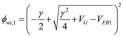 (27)
(27)
and  (28)
(28)
For strong inversion region (VG > Vt) or ( > 2
> 2 + V), the exponential term in Equation (25) becomes dominant. A fairly accurate approximate expression of surface potential in this region can be obtained by considering all the
  apart from the dominant exponential term of Equation (26) to be constant at a value of 2
 + V. Thus,
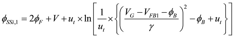 (29)
(29)
For conduction in the s-Si/SiGe interface, the depletion region should lie between VFB2 and Vt, since below VFB2, holes start to accumulate at the strained-Si/SiGe interface. Thus the regional depletion charge from Poissons solution is given by
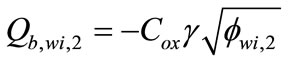 (30)
(30)
where 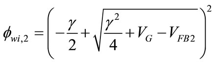 (31)
(31)
As for the other interface, a smoothing parameter is used to avoid negative square roots in the equation for surface potential and to make it continuous with the accumulation region. However, we have not included the accumulation region yet in our model. On similar lines, for strong inversion region,
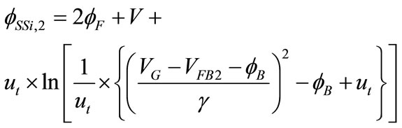 (32)
(32)
For any interface, at any region total current is the sum of the drift component (Idrift) and the diffusion component (Idiff) with the surface potential being used in the relations corresponding to the regions of weak or strong inversion for the different interfaces. For the calculation of the drain current Ids, the stress induced mobility μ have been taken [35]. Again under the assumption of the gradual channel approximation and the charge sheet approximation, the drain current may be written as [36-38]:
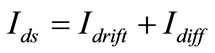 (33)
(33)
where the drift component Idrift and diffusion component Idiff are given by:
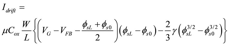 (34)
(34)
and
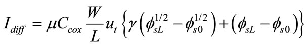 (35)
(35)
Here  and
and  denote the electrostatic surface potential at the source and drain side, respectively and required to calculate Ids, are obtained numerically under the following boundary conditions
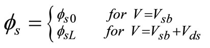 (36)
(36)
where Vsb and Vds are the source to substrate and drain voltage, respectively. In sub-threshold region,  is almost equal to
 , and even a small error in the value of
  and
and  can lead to a large error in the diffusion current (Idiff), which depends on difference of
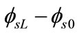 . Therefore, an accurate value is required for surface potential, particularly for current calculations. With the help of Equation (26), the above difficulty can be simplified by rewriting Equation (35) as:
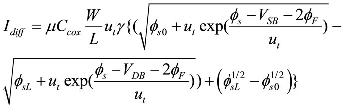 (37)
(37)
In our model, we have considered the two drain-current components separately, i.e.,  at the 2-DEG in SiGe and
  at the strained-Si/SiO2 interface.
1) Current in the 2-DEG in SiGe : The dominant component of the current in the weak inversion region is due to the diffusion of electrons in SiGe layer and in strong inversion region is due to the drift of electrons in the 2-DEG in SiGe due to the application of a drain voltage (Vds). When the current flows in SiGe layer, the channel potential with respect to the source rises continuously from source to the drain. For VFB1 < VG < VFB2, current is dominated only by diffusion component.
2) Current at the strained-Si/SiO2 Interface : The dominant component of the current in the weak inversion region is due to the diffusion of electrons in strained-Si layer and in strong inversion region is due to the drift of electrons in the 2-DEG in strained-Si due to the application of a drain voltage (Vds). When the current flows in strained-Si layer, the channel potential with respect to the source rises continuously from source to the drain. When VFB2 < VG < VTSiGe, the diffusion components of current in strained-Si and SiGe layer are dominant. VTSiGe is the threshold voltage for strained-Si/SiGe heterolayers.
So, 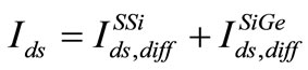 (38)
(38)
Now, we consider a threshold voltage for the channel at the strained-Si/SiO2 interface denoted by VTSSi which is defined as the gate voltage at which the potential at the strained-Si/SiO2 interface is equal to 2 . For VTSiGe < VG < VTSSi current is flowing for the drift component of the current in SiGe layer and diffusion component of current in strained-Si layer. Thus
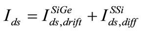 (39)
(39)
Also, for VG > VTSSi drift currents flow through both the layers in the strong inversion region. Hence
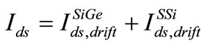 (40)
(40)
4. Results and Discussion
The surface potential  as a function of gate voltage (VG) for bulk-Si and strained-Si MOSFETs are shown in Figure 3. To reduce the computational time and maintain the accuracy, an explicit description of surface potential with regional approximations has to be made to Equation (25). A distinction can be made between weak inversion and strong inversion, as indicated in Figure 3. In the weak inversion region 0 <
  < 2
< 2 + VG, the exponential term in Equation (25) is negligible as shown in Equations (27) and (31). In the strong inversion region,
  > 2
> 2 + VG and the exponential term in Equation (25) becomes dominant. Accurate expression for surface potential in strong inversion is expressed in Equations (29) and (32) [35]. The surface potential becomes practically independent of high gate voltage and become saturate.
The drain current for an ideal long-channel MOSFET given by Equations (38), (39) and (40), has been calculated using surface potential values. The complete current-voltage (Ids-VG) characteristics obtained using the surface potential model (dashed-dot lines), are shown in Figure 4. The figure shows the drain current (Ids) and its component diffusion current (Idiff) and drift current (Idrift),
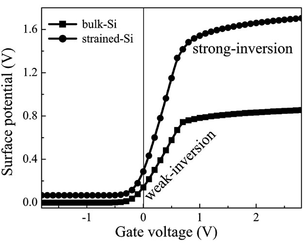
Figure 3. The electrostatic surface potential Φs as a function of gate voltage VG. The results of the weak and strong inversion approximation are shown for bulk-Si and strained-Si MOSFETs.
as a function of VG at Vds = 0.1 V and Vsb = 0 V. As can be seen from the figure, in strong inversion Ids ≈ Idrift (dotted line) so that the current is mainly due to drift velocity of electrons. In weak inversion Ids ≈ Idift (dotted line) and the current is mainly due to diffusion of electrons.
The model has been successfully implemented in MATLAB. To validate our model, the results obtained from MATLAB are compared with the simulated data obtained using Sentaurus device simulator [34]. Figure 5 shows current-voltage characteristics comparison between the results obtained from the model with results obtained from Sentaurus simulation. In practice, however, the electrical characteristics of a MOSFET deviate from the simulated behavior. This is due to the fact that various physical effects, such as, mobility reduction, velocity saturation, series resistance, channel length modulation, static feedback, drain induced barrier lowering and weak-avalanche amongst others can be fully captured in simulation. In the following, we develop the drain current model for strained-Si nMOSFETs based on regional approximations to circumvent the implicit relations for Φs discussed above. This is done by separately modeling weak and strong inversion regions. However, there is a region between the weak and strong inversion, called the moderate inversion, where both the drift and diffusion components are important and this region can be easily modeled using a smoothing function [39]. We have employed polynomial fits to get good accuracy in moderate inversion region. A close match is found with simulated data considering 4th order polynomial fit. This type of model can be used for circuit simulation because of its simplicity and accuracy. Device simulations have been performed using Sentaurus device tool [34]. The transport parameters used in the drift-diffusion simulation have been taken from the Strained-Silicon.par parameter file.
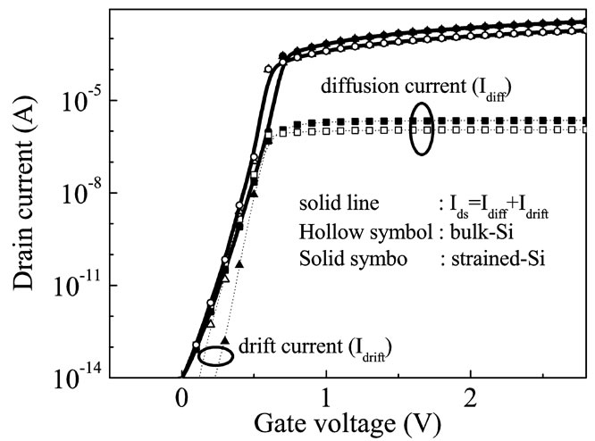
Figure 4. The drain current as a function of gate voltage (VG) based on surface-potential model. Diffusion current (Idiff), drift current (Idrift), and total current (Ids = Idiff + Idrift) for both bulk-Si and strained-Si MOSFETs.
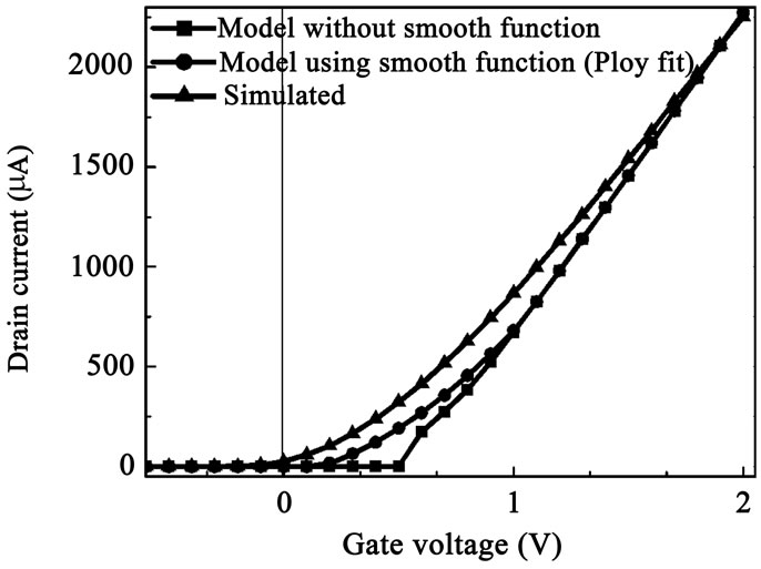
Figure 5. Comparison of current-voltage characteristics obtained from the model developed with results obtained from Sentaurus simulation.
5. Conclusions
A charge sheet surface potential based analytical model for strained-Si MOSFETs is presented and validated with numerical simulation. The model considers the sub band splitting in the 2-DEG at the top heterointerface in the SiGe layer and also the heterointerface at the strainedSi/SiO2 interface. The model is scalable with strained-Si material parameters with physically derived flat band voltages. The model is developed based on the regional charge-based approach, where regional solutions are physically derived. The developed model may be used for circuit simulation involving strained-Si MOSFETs for the next generation ULSI circuits. The modeling of ultra-short (below 90 nm) channel strained-Si devices, however, will require further developments on precise description of physical effects such as series resistance, velocity saturation, channel length modulation, static feedback, self-heating and drain induced barrier lowering.
6. REFERENCES
- Semiconductor Industry Association, “International Technology Roadmap for Semiconductors,” SIA, San Jose, 2005.
- C. K. Maiti, S. Chattopadhyay and L. K. Bea, “Strained-Si Heterostructure Field Effect Device,” Taylor & Francis Group LLC, Boca Raton, 2007.
- C. K. Maiti and G. A. Armstrong, “Applications of Silicon-Germanium Heterostructure Devices,” Institute of Physics Publisher, Bristol, 2001.
- J. L. Hoyt, H. M. Nayfeh, S. Eguchi, I. Aberg, G. Xia, T. Drake, E. A. Fitzgerald and D. A. Antoniadis, “Strained Silicon MOSFET Technology,” IEEE International Electron Devices Meeting Technical Digest, San Francisco, 8-11 December 2002, pp. 23-26.
- R. W. Keyes, “Explaining Strain in Silicon,” IEEE Circuits & Devices Magazine, Vol. 35, 2002, pp. 36-39.
- J. Welser, J. L. Hoyt, S. Takagi and J. F. Gibbons, “Strain Dependence of the Performance Enhancement in Strained-Si n-MOSFETs,” IEEE International Electron Devices Meeting Technical Digest, San Francisco, 11-14 December 1994, pp. 373-376.
- C. K. Maiti, “Editorial, Special Issue on Strained-Si Heterostructures and Devices,” Solid-State Electronics, Vol. 48, 2004, p. 1255.
- C. K. Maiti, L. K. Bera and S. Chattopadhyay, “Strained-Si Heterostructure Field Effect Transistors,” Semiconductor Science and Technology, Vol. 13, No. 11, 1998, pp. 1225- 1246.
- S.-I. Takagi, T. Mizuno, T. Tezuka, N. Sugiyama, S. Nakaharai, T. Numata, J. Koga and K. Uchida, “SubBand Structure Engineering for Advanced CMOS Channels,” Solid-State Electronics, Vol. 49, No. 5, 2005, pp. 684-694.
- F. Schaffler, “High-Mobility Si and Ge Structures,” Semiconductor Science and Technology, Vol. 12, No. 12, 1997, pp. 1515-1549.
- J. Welser, J. L. Hoyt and J. F. Gibbons, “Electron Mobility Enhancement in Strained-Si N-Type Metal-OxideSemiconductor Field-Effect Transistors,” IEEE Electron Device Letters, Vol. 15, No. 3, 1994, pp. 100-102.
- D. K. Nayak, J. C. S. Woo, J. S. Park, K. L. Wang and K. P. Macwilliams, “High-Mobility p-Channel Metal-OxideSemiconductor Field-Effect Transistor on Strained Si,” Applied Physics Letters, Vol. 62, No. 22, 1993, pp. 2853- 2855.
- M. V. Fischetti and S. E. Laux, “Band Structure, Deformation Potentials, and Carrier Mobility in Strained Si, Ge, and SiGe Alloys,” Journal of Applied Physics, Vol. 88, No. 4, 1996, pp. 2234-2252.
- R. Oberhuber, G. Zandler and P. Vogl, “Subband Structure and Mobility of Two-Dimensional Holes in Strained Si/SiGe MOSFETs,” Physical Review B, Vol. 58, No. 15, 1998, pp. 9941-9948.
- C. K. Maiti, S. K. Samanta, S. Chatterjee, G. K. Dalapati and L. K. Bera, “Gate Dielectrics on Strained-Si/SiGe Heterolayers,” Solid-State Electronics, Vol. 48, No. 8, 2004, pp. 1369-1389.
- K. Joardar, K. K. Gullapalli, C. McAndrew, M. E. Burnham and A. Wild, “An Improved MOSFET Model for Circuit Simulation,” IEEE Transactions on Electron Devices, Vol. 45, No. 1, January 1998, pp. 134-148.
- P. Bendix, P. Rakers, P. Wagh, L. Lemaitre, W. Grabinski, C. C. McAndrew, X. Gu and G. Gildenblat, “RF Distortion Analysis with Compact MOSFET Models,” Proceedings of IEEE Custom Integrated Circuits Conference, Orlando, 3-6 October 2004, pp. 9-12.
- “BSIM3 and BSIM4 Compact MOSFET Model Summary.” http://www-device.eecs.berkeley.edu/~3/get.html
- C. C. Enz, F. Krummenacher and E. A. Vittoz, “An Analytical MOS Transistor Model Valid in All Regions of Operation and Dedicated to Low-Voltage and Low-Current Applications,” Analog Integrated Circuits and Signal Processing, Vol. 8, No. 1, July 1995, pp. 83-114.
- G. Gildenblat, X. Li, W. Wu, H. Wang, A. Jha, R. Van Langevelde, G. Smit, A. Scholten and D. Klassen, “PSP: An Advanced Surface Potential Based MOSFET Model for Circuit Simulation,” IEEE Transactions on Electron Devices, Vol. 53, No. 9, September 2006, pp. 399-402.
- T.-L. Chen and G. Gildenblat, “Symmetric Bulk Charge Linearization of Charge Sheet MOSFET Model,” Electronics Letters, Vol. 37, No. 12, June 2001, pp. 791-793.
- T.-L. Chen and G. Gildenblat, “Analytical Approximation for the MOSFET Surface Potential,” Solid-State Electronics, Vol. 45, No. 2, February 2001, pp. 335-339.
- M. M. Mattausch, U. Feldmann, A. Rahm, M. Bollu and D. Savignac, “Unified Complete MOSFET Model for Circuit for Analysis of Digital and Analog Circuits,” IEEE Transactions on Computer-Aided Design of Integrated Circuits and Systems, Vol. 15, No. 1, January 1996, pp. 1-7.
- W. Zhang and J. G. Fossum, “On the Threshold Voltage of Strained-Si–Si1 – xGex MOSFETs,” IEEE Transactions on Electron Devices, Vol. 52, No. 2, February 2005, pp. 263-268.
- K. Chandrasekaran, X. Zhou, S. B. Chiah, W. Shangguan and G. H. See, “Physics-Based Single-Piece Charge Model for Strained-Si MOSFETs,” IEEE Transactions on Electron Devices, Vol. 52, No. 7, July 2005, pp. 1555-1562.
- B. Bindu, N. DasGupta and A. DasGupta, “Analytical Model of Drain Current of Si/SiGe Heterostructure p-Channel MOSFETs for Circuit Simulation,” IEEE Transactions on Electron Devices, Vol. 53, No. 6, June 2006, pp. 1411-1419.
- Y. L. Tsang, S. Chattopadhyay, S. Uppal, E. Escobedo-Cousin, H. Ramakrishnan, S. H. Olsen and A. G. O’Neill, “Modeling of the Threshold Voltage in Strained Si/Si1 − xGex/Si1 − yGey(x ≥ y) CMOS Architectures,” IEEE Transactions on Electron Devices, Vol. 54, No. 11, November 2007, pp. 3040-3048.
- E. Kasper and D. J. Paul, “Silicon Quantum Integrated Circuits,” Springer-Verlag, Berlin, 2005.
- M. M. Rieger and P. Vogl, “Electronic-Band Parameters in Strained Si1 – xGex Alloys on Si1 – yGey Substrate,” Physical Review B, Vol. 48, No. 19, 1993, pp. 14276- 14287.
- L. Yang, J. Watling, M. Borici, R. C. W. Wilkins, A. Asenov, J. R. Barker and S. Roy, “Simulations of Scaled Sub-100 nm Strained Si/SiGe p-Channel MOSFETs,” Journal of Computational Electronics, Vol. 2, 2004, pp. 363-368.
- L. Yang, J. R. Watling, R. C. W. Wilkins, M. Borici, J. R. Barker, A. Asenov and S. Roy, “Si/SiGe Heterostructure Parameters for Device Simulations,” Semiconductor Science and Technology, Vol. 19, No. 10, 2004, pp. 1174- 1182.
- R. People and J. C. Bean, “Band Alignments of Coherently Strained GexSi1 – x/Si Heterostructures on <001> GeySi1 – y Substrates,” Applied Physics Letters, Vol. 48, 1986, pp. 538-541.
- M. M. Rieger and P. Vogl, “Electronic Band Parameters in Strained Si1 – xGex Alloys on Si1 – yGey Substrates,” Physical Review B, Condensed Matter, Vol. 48, No. 19, pp. 14276-14276, 1993.
- Synopsys, Inc., “Sentaurus Device User Guide,” Version A-2008.09, Synopsys, Inc., Mountain View, 2008.
- J. L. Egley and D. Chidambarrao, “Strain Effects on Device Characteristics: Implementation in Drift-Diffusion Simulators,” Solid-State Electronics, Vol. 36, No. 12, 1993, pp. 1653-1664.
- N. D. Arora, “MOSFET Models for VLSI Circuit Simulation,” Springer-Verlag, New York, 1993.
- H. C. de Graaff and F. M. Klaassen, “Compact Transistor Modelling for Circuit Design,” Springer-Verlag, New York, 1990.
- J. R. Brews, “A Charge-Sheet Model of the MOSFET,” Solid-State Electronics, Vol. 21, No. 2, 1978, pp. 345- 355.
- R. V. Langevelde and F. M. Klaassen, “An Explicit Surface-Potential-Based MOSFET Model for Circuit Simulation,” Solid-State Electronics, Vol. 44, No. 3, 2000, pp. 409-418.