Paper Menu >>
Journal Menu >>
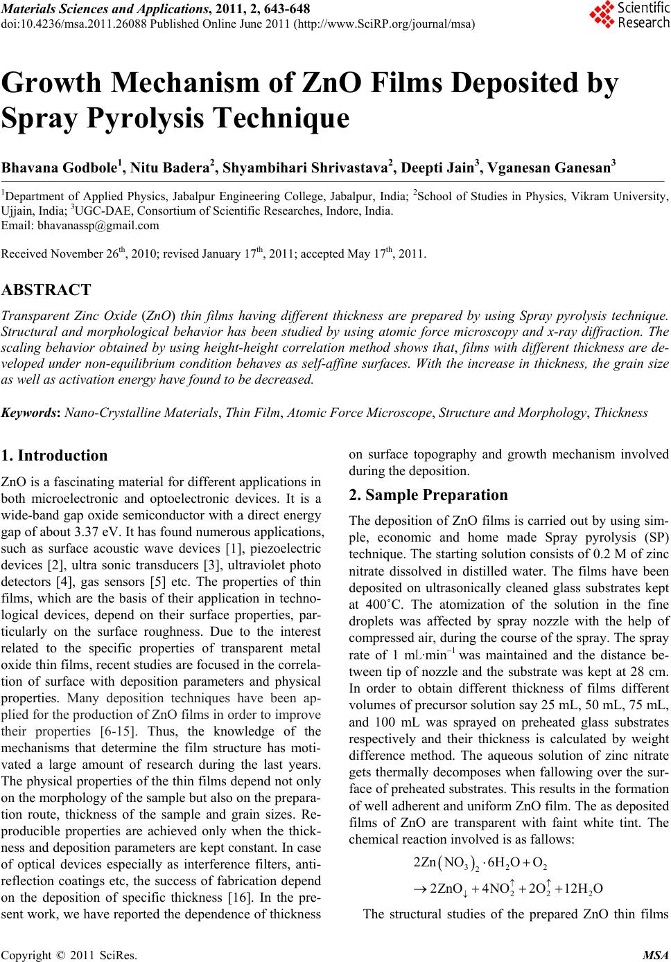 Materials Sciences and Applicatio ns, 2011, 2, 643-648 doi:10.4236/msa.2011.26088 Published Online June 2011 (http://www.SciRP.org/journal/msa) Copyright © 2011 SciRes. MSA 643 Growth Mechanism of ZnO Films Deposited by Spray Pyrolysis Technique Bhavana Godbole1, Nitu Badera2, Shyambihari Shrivastava2, Deepti Jain3, Vganesan Ganesan3 1Department of Applied Physics, Jabalpur Engineering College, Jabalpur, India; 2School of Studies in Physics, Vikram University, Ujjain, India; 3UGC-DAE, Consortium of Scientific Researches, Indore, India. Email: bhavanassp@gmail.com Received November 26th, 2010; revised January 17th, 2011; accepted May 17th, 2011. ABSTRACT Transparent Zinc Oxide (ZnO) thin films having different thickness are prepared by using Spray pyrolysis technique. Structural and morphological behavior has been studied by using atomic force microscopy and x-ray diffraction. The scaling behavior obtained by using height-height correlation method shows that, films with different thickness are de- veloped under non-equilibrium condition behaves as self-affine surfaces. With the increase in thickness, the grain size as well as activation energy have found to be decreased. Keywords: Nano-Crystalline Materials, Thin Film, Atomic Force Microscope, Structure and Morphology, Thickness 1. Introduction ZnO is a fascinating material for different applications in both microelectronic and optoelectronic devices. It is a wide-band gap oxide semiconductor with a direct energy gap of about 3.37 eV. It has found numerous applications, such as surface acoustic wave devices [1], piezoelectric devices [2], ultra sonic transducers [3], ultraviolet photo detectors [4], gas sensors [5] etc. The properties of thin films, which are the basis of their application in techno- logical devices, depend on their surface properties, par- ticularly on the surface roughness. Due to the interest related to the specific properties of transparent metal oxide thin films, recent studies are focused in the correla- tion of surface with deposition parameters and physical properties. Many deposition techniques have been ap- plied for the production of ZnO films in order to improve their properties [6-15]. Thus, the knowledge of the mechanisms that determine the film structure has moti- vated a large amount of research during the last years. The physical properties of the thin films depend not only on the morphology of the sample but also on the prepara- tion route, thickness of the sample and grain sizes. Re- producible properties are achieved only when the thick- ness and deposition parameters are kept constant. In case of optical devices especially as interference filters, anti- reflection coatings etc, the success of fabrication depend on the deposition of specific thickness [16]. In the pre- sent work, we have reported the dependence of thickness on surface topography and growth mechanism involved during the deposition. 2. Sample Preparation The deposition of ZnO films is carried out by using sim- ple, economic and home made Spray pyrolysis (SP) technique. The starting solution consists of 0.2 M of zinc nitrate dissolved in distilled water. The films have been deposited on ultrasonically cleaned glass substrates kept at 400˚C. The atomization of the solution in the fine droplets was affected by spray nozzle with the help of compressed air, during the course of the spray. The spray rate of 1 mL·min–1 was maintained and the distance be- tween tip of nozzle and the substrate was kept at 28 cm. In order to obtain different thickness of films different volumes of precursor solution say 25 mL, 50 mL, 75 mL, and 100 mL was sprayed on preheated glass substrates respectively and their thickness is calculated by weight difference method. The aqueous solution of zinc nitrate gets thermally decomposes when fallowing over the sur- face of preheated substrates. This results in the formation of well adherent and uniform ZnO film. The as deposited films of ZnO are transparent with faint white tint. The chemical reaction involved is as fallows: 322 2 22 2 2ZnNO6HOO 2ZnO4NO2O12HO The structural studies of the prepared ZnO thin films 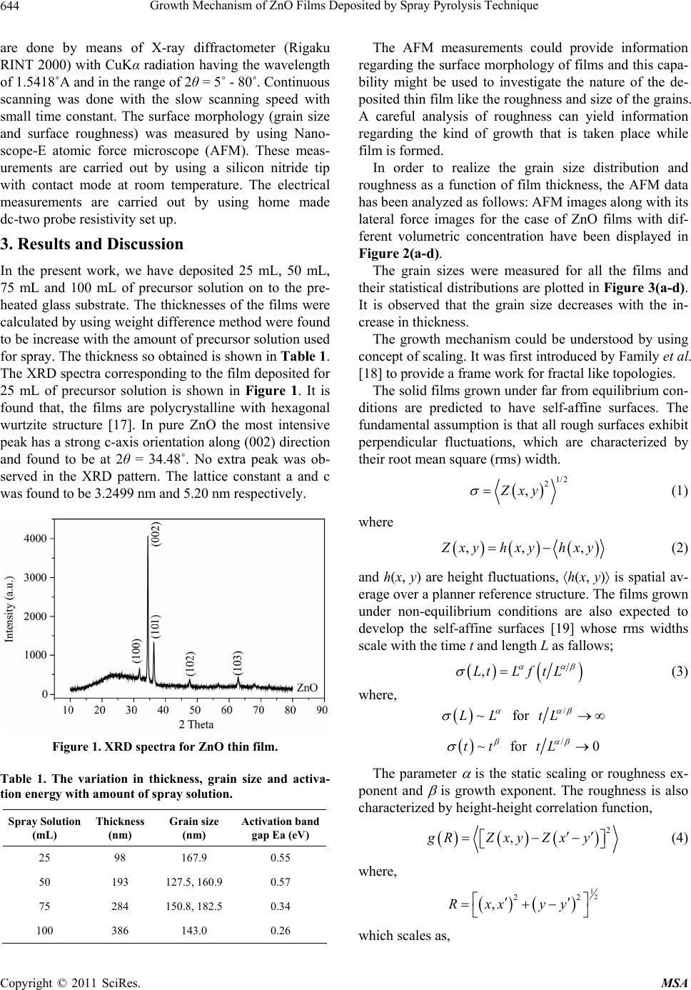 Growth Mechanism of ZnO Films Deposited by Spray Pyrolysis Technique 644 are done by means of X-ray diffractometer (Rigaku RINT 2000) with CuKα radiation having the wavelength of 1.5418˚A and in the range of 2θ = 5˚ - 80˚. Continuous scanning was done with the slow scanning speed with small time constant. The surface morphology (grain size and surface roughness) was measured by using Nano- scope-E atomic force microscope (AFM). These meas- urements are carried out by using a silicon nitride tip with contact mode at room temperature. The electrical measurements are carried out by using home made dc-two probe resistivity set up. 3. Results and Discussion In the present work, we have deposited 25 mL, 50 mL, 75 mL and 100 mL of precursor solution on to the pre- heated glass substrate. The thicknesses of the films were calculated by using weight difference method were found to be increase with the amount of precursor solution used for spray. The thickness so obtained is shown in Table 1. The XRD spectra corresponding to the film deposited for 25 mL of precursor solution is shown in Figure 1. It is found that, the films are polycrystalline with hexagonal wurtzite structure [17]. In pure ZnO the most intensive peak has a strong c-axis orientation along (002) direction and found to be at 2θ = 34.48˚. No extra peak was ob- served in the XRD pattern. The lattice constant a and c was found to be 3.2499 nm and 5.20 nm respectively. Figure 1. XRD spectra for ZnO thin film. Table 1. The variation in thickness, grain size and activa- tion energy with amount of spray solution. Spray Solution (mL) Thickness (nm) Grain size (nm) Activation band gap Ea (eV) 25 98 167.9 0.55 50 193 127.5, 160.9 0.57 75 284 150.8, 182.5 0.34 100 386 143.0 0.26 The AFM measurements could provide information regarding the surface morphology of films and this capa- bility might be used to investigate the nature of the de- posited thin film like the roughness and size of the grains. A careful analysis of roughness can yield information regarding the kind of growth that is taken place while film is formed. In order to realize the grain size distribution and roughness as a function of film thickness, the AFM data has been analyzed as follows: AFM images along with its lateral force images for the case of ZnO films with dif- ferent volumetric concentration have been displayed in Figure 2(a-d). The grain sizes were measured for all the films and their statistical distributions are plotted in Figure 3(a-d). It is observed that the grain size decreases with the in- crease in thickness. The growth mechanism could be understood by using concept of scaling. It was first introduced by Family et al. [18] to provide a frame work for fractal like topologies. The solid films grown under far from equilibrium con- ditions are predicted to have self-affine surfaces. The fundamental assumption is that all rough surfaces exhibit perpendicular fluctuations, which are characterized by their root mean square (rms) width. 1/2 2 ,Zxy (1) where ,, , Z xy hxyhxy (2) and h(x, y) are height fluctuations, h(x, y) is spatial av- erage over a planner reference structure. The films grown under non-equilibrium conditions are also expected to develop the self-affine surfaces [19] whose rms widths scale with the time t and length L as fallows; ,LtLft L (3) where, ~LL for / tL ~tt for /0tL The parameter is the static scaling or roughness ex- ponent and is growth exponent. The roughness is also characterized by height-height correlation function, 2 ,gRZxyZx y (4) where, 12 22 ,Rxx yy which scales as, Copyright © 2011 SciRes. MSA 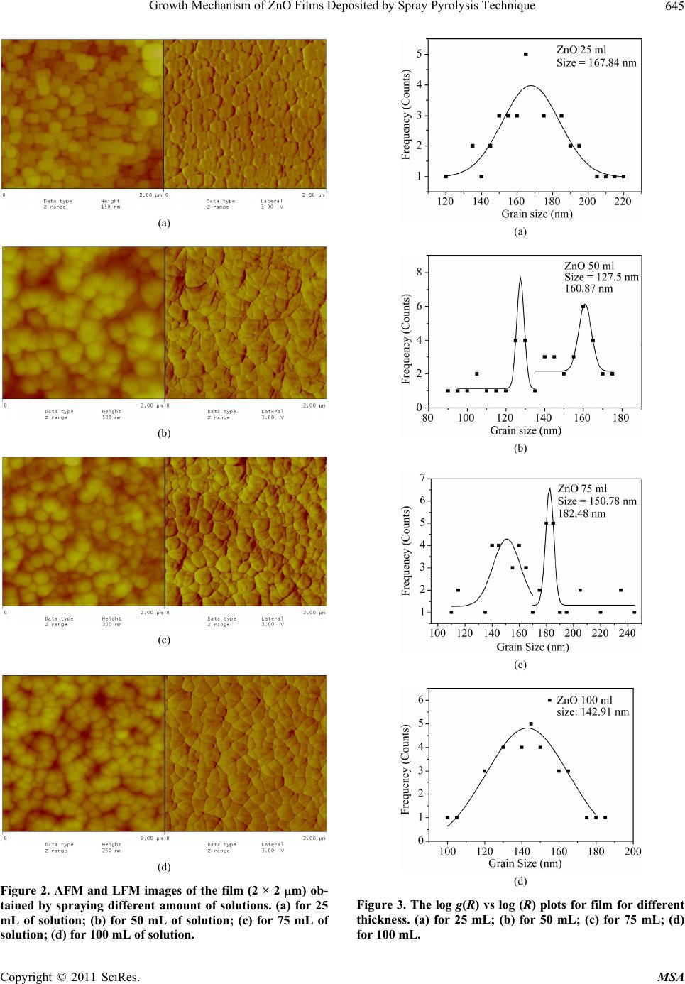 Growth Mechanism of ZnO Films Deposited by Spray Pyrolysis Technique645 (a) (b) (c) (d) Figure 2. AFM and LFM images of the film (2 × 2 m) ob- tained by spraying different amount of solutions. (a) for 25 mL of solution; (b) for 50 mL of solution; (c) for 75 mL of solution; (d) for 100 mL of solution. (a) (b) (c) (d) Figure 3. The log g(R) vs log (R) plots for film for different thickness. (a) for 25 mL; (b) for 50 mL; (c) for 75 mL; (d) for 100 mL. Copyright © 2011 SciRes. MSA 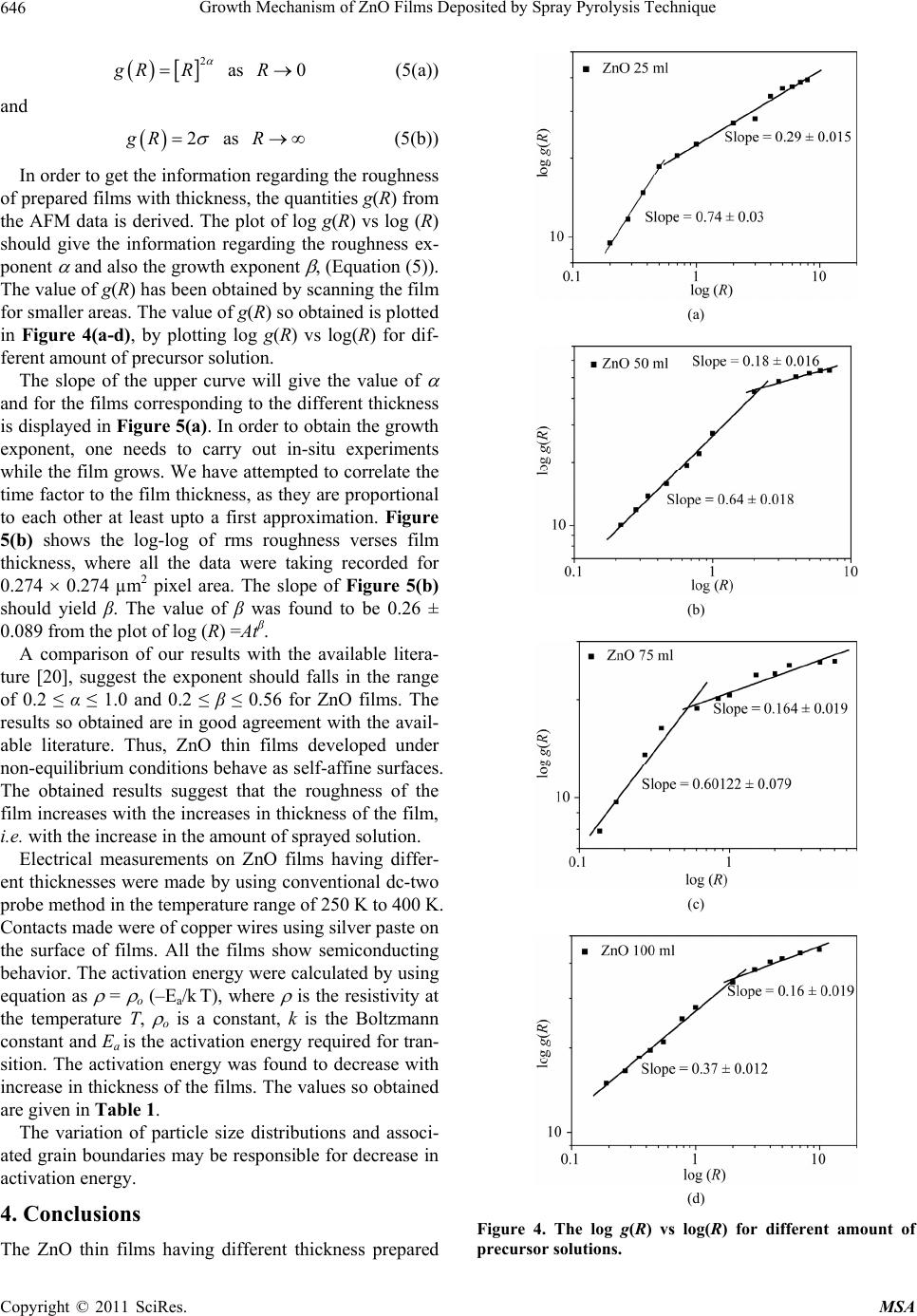 Growth Mechanism of ZnO Films Deposited by Spray Pyrolysis Technique 646 2 g RR as (5(a)) 0R and 2gR as (5(b)) R In order to get the information regarding the roughness of prepared films with thickness, the quantities g(R) from the AFM data is derived. The plot of log g(R) vs log (R) should give the information regarding the roughness ex- ponent and also the growth exponent , (Equation (5)). The value of g(R) has been obtained by scanning the film for smaller areas. The value of g(R) so obtained is plotted in Figure 4(a-d), by plotting log g(R) vs log(R) for dif- ferent amount of precursor solution. The slope of the upper curve will give the value of and for the films corresponding to the different thickness is displayed in Figure 5(a). In order to obtain the growth exponent, one needs to carry out in-situ experiments while the film grows. We have attempted to correlate the time factor to the film thickness, as they are proportional to each other at least upto a first approximation. Figure 5(b) shows the log-log of rms roughness verses film thickness, where all the data were taking recorded for 0.274 0.274 µm2 pixel area. The slope of Figure 5(b) should yield β. The value of β was found to be 0.26 ± 0.089 from the plot of log (R) =Atβ. A comparison of our results with the available litera- ture [20], suggest the exponent should falls in the range of 0.2 ≤ α ≤ 1.0 and 0.2 ≤ β ≤ 0.56 for ZnO films. The results so obtained are in good agreement with the avail- able literature. Thus, ZnO thin films developed under non-equilibrium conditions behave as self-affine surfaces. The obtained results suggest that the roughness of the film increases with the increases in thickness of the film, i.e. with the increase in the amount of sprayed solution. Electrical measurements on ZnO films having differ- ent thicknesses were made by using conventional dc-two probe method in the temperature range of 250 K to 400 K. Contacts made were of copper wires using silver paste on the surface of films. All the films show semiconducting behavior. The activation energy were calculated by using equation as = o (–Ea/k T), where is the resistivity at the temperature T, o is a constant, k is the Boltzmann constant and Ea is the activation energy required for tran- sition. The activation energy was found to decrease with increase in thickness of the films. The values so obtained are given in Table 1. The variation of particle size distributions and associ- ated grain boundaries may be responsible for decrease in activation energy. 4. Conclusions The ZnO thin films having different thickness prepared (a) (b) (c) (d) Figure 4. The log g(R) vs log(R) for different amount of precursor solutions. Copyright © 2011 SciRes. MSA 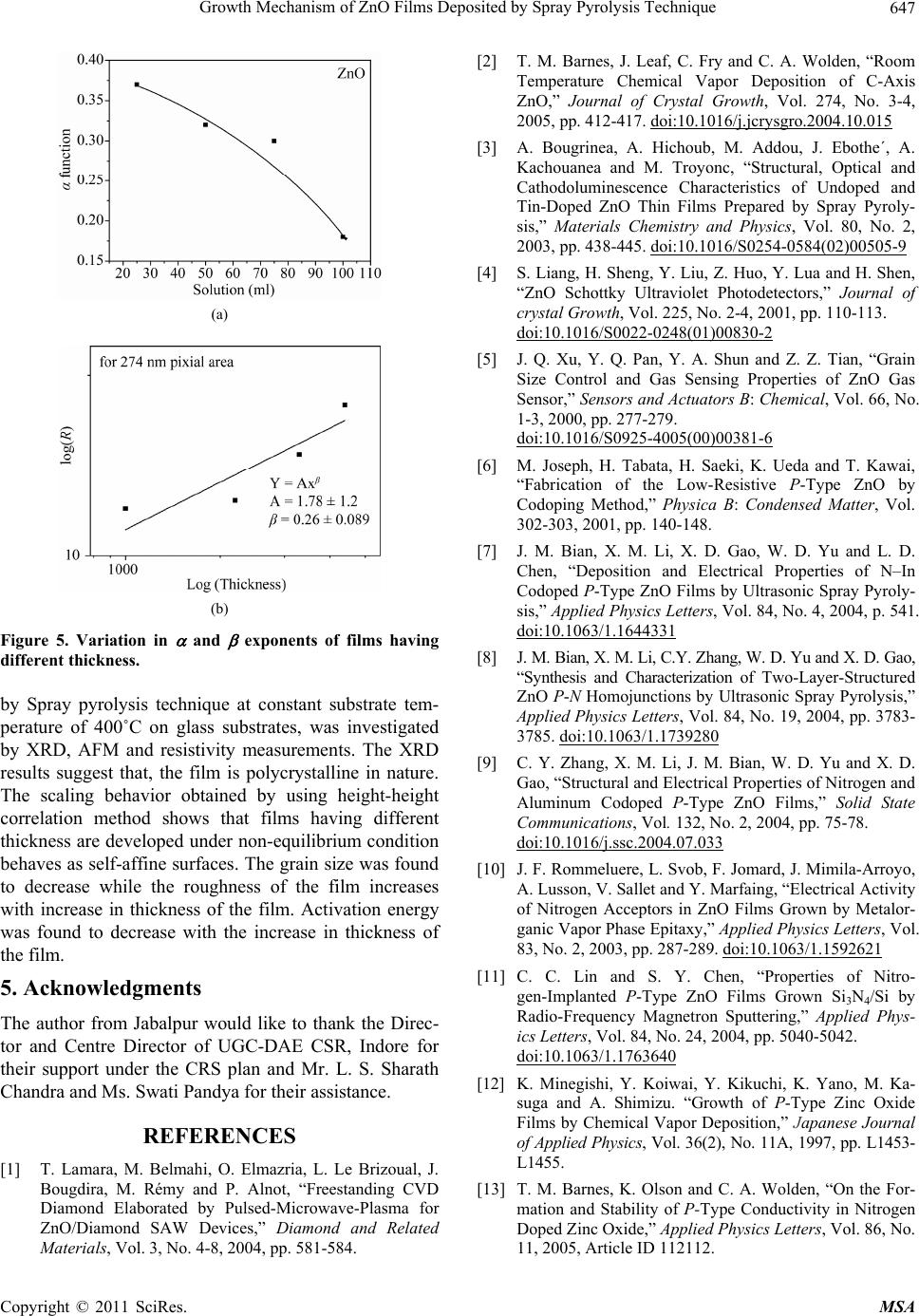 Growth Mechanism of ZnO Films Deposited by Spray Pyrolysis Technique647 (a) (b) Figure 5. Variation in and exponents of films having different thickness. by Spray pyrolysis technique at constant substrate tem- perature of 400˚C on glass substrates, was investigated by XRD, AFM and resistivity measurements. The XRD results suggest that, the film is polycrystalline in nature. The scaling behavior obtained by using height-height correlation method shows that films having different thickness are developed under non-equilibrium condition behaves as self-affine surfaces. The grain size was found to decrease while the roughness of the film increases with increase in thickness of the film. Activation energy was found to decrease with the increase in thickness of the film. 5. Acknowledgments The author from Jabalpur would like to thank the Direc- tor and Centre Director of UGC-DAE CSR, Indore for their support under the CRS plan and Mr. L. S. Sharath Chandra and Ms. Swati Pandya for their assistance. REFERENCES [1] T. Lamara, M. Belmahi, O. Elmazria, L. Le Brizoual, J. Bougdira, M. Rémy and P. Alnot, “Freestanding CVD Diamond Elaborated by Pulsed-Microwave-Plasma for ZnO/Diamond SAW Devices,” Diamond and Related Materials, Vol. 3, No. 4-8, 2004, pp. 581-584. [2] T. M. Barnes, J. Leaf, C. Fry and C. A. Wolden, “Room Temperature Chemical Vapor Deposition of C-Axis ZnO,” Journal of Crystal Growth, Vol. 274, No. 3-4, 2005, pp. 412-417. doi:10.1016/j.jcrysgro.2004.10.015 [3] A. Bougrinea, A. Hichoub, M. Addou, J. Ebothe´, A. Kachouanea and M. Troyonc, “Structural, Optical and Cathodoluminescence Characteristics of Undoped and Tin-Doped ZnO Thin Films Prepared by Spray Pyroly- sis,” Materials Chemistry and Physics, Vol. 80, No. 2, 2003, pp. 438-445. doi:10.1016/S0254-0584(02)00505-9 [4] S. Liang, H. Sheng, Y. Liu, Z. Huo, Y. Lua and H. Shen, “ZnO Schottky Ultraviolet Photodetectors,” Journal of crystal Growth, Vol. 225, No. 2-4, 2001, pp. 110-113. doi:10.1016/S0022-0248(01)00830-2 [5] J. Q. Xu, Y. Q. Pan, Y. A. Shun and Z. Z. Tian, “Grain Size Control and Gas Sensing Properties of ZnO Gas Sensor,” Sensors and Actuators B: Chemical, Vol. 66, No. 1-3, 2000, pp. 277-279. doi:10.1016/S0925-4005(00)00381-6 [6] M. Joseph, H. Tabata, H. Saeki, K. Ueda and T. Kawai, “Fabrication of the Low-Resistive P-Type ZnO by Codoping Method,” Physica B: Condensed Matter, Vol. 302-303, 2001, pp. 140-148. [7] J. M. Bian, X. M. Li, X. D. Gao, W. D. Yu and L. D. Chen, “Deposition and Electrical Properties of N–In Codoped P-Type ZnO Films by Ultrasonic Spray Pyroly- sis,” Applied Physics Letters, Vol. 84, No. 4, 2004, p. 541. doi:10.1063/1.1644331 [8] J. M. Bian, X. M. Li, C.Y. Zhang, W. D. Yu and X. D. Gao, “Synthesis and Characterization of Two-Layer-Structured ZnO P-N Homojunctions by Ultrasonic Spray Pyrolysis,” Applied Physics Letters, Vol. 84, No. 19, 2004, pp. 3783- 3785. doi:10.1063/1.1739280 [9] C. Y. Zhang, X. M. Li, J. M. Bian, W. D. Yu and X. D. Gao, “Structural and Electrical Properties of Nitrogen and Aluminum Codoped P-Type ZnO Films,” Solid State Communications, Vol. 132, No. 2, 2004, pp. 75-78. doi:10.1016/j.ssc.2004.07.033 [10] J. F. Rommeluere, L. Svob, F. Jomard, J. Mimila-Arroyo, A. Lusson, V. Sallet and Y. Marfaing, “Electrical Activity of Nitrogen Acceptors in ZnO Films Grown by Metalor- ganic Vapor Phase Epitaxy,” Applied Physics Letters, Vol. 83, No. 2, 2003, pp. 287-289. doi:10.1063/1.1592621 [11] C. C. Lin and S. Y. Chen, “Properties of Nitro- gen-Implanted P-Type ZnO Films Grown Si3N4/Si by Radio-Frequency Magnetron Sputtering,” Applied Phys- ics Letters, Vol. 84, No. 24, 2004, pp. 5040-5042. doi:10.1063/1.1763640 [12] K. Minegishi, Y. Koiwai, Y. Kikuchi, K. Yano, M. Ka- suga and A. Shimizu. “Growth of P-Type Zinc Oxide Films by Chemical Vapor Deposition,” Japanese Journal of Applied Physics, Vol. 36(2), No. 11A, 1997, pp. L1453- L1455. [13] T. M. Barnes, K. Olson and C. A. Wolden, “On the For- mation and Stability of P-Type Conductivity in Nitrogen Doped Zinc Oxide,” Applied Physics Letters, Vol. 86, No. 11, 2005, Article ID 112112. Copyright © 2011 SciRes. MSA  Growth Mechanism of ZnO Films Deposited by Spray Pyrolysis Technique Copyright © 2011 SciRes. MSA 648 [14] G. K. Paul and S. K. Sen, “Sol-Gel Preparation, Charac- terization and Studies on Electrical and Thermoelectrical Properties of Gallium Doped Zinc Oxide Films,” Materials Letters, Vol. 57, No. 3, 2002, pp. 742-746. doi:10.1016/S0167-577X(02)00865-0 [15] J. M. Bian, X. M. Li, C. Y. Zhang, W. D. Yu and X. D. Gao, “P-Type ZnO Films by Monodoping of Nitrogen and ZnO-Based P-N Homojunctions,” Applied Physics Letters, Vol. 85, No. 18, 2004, pp. 4070-4072. doi:10.1063/1.1808229 [16] M. Suchea and Kiriakidis, “Surface Characterization of ZnO Transparent Thin Films,” Journal of Physics: Con- ference Series, Vol. 10, No. 10, 2005, pp. 147-150. doi:10.1088/1742-6596/10/1/036 [17] F. Matsukura, H. Ohno, A. Shen and Y. Sugawara, “Transport Propertiesand Origin of Ferromagnetism in (Ga Mn) As,” Physical Review B, Vol. 57, No. 4, 1998, p. R2037. doi:10.1103/PhysRevB.57.R2037 [18] F. Family, “Dynamic Scaling and Phase-Transitions in Interface Growth,” Physica A: Statistical Mechanics and Its Applications, Vol. 168, No. 1, 1990, pp. 561. [19] M. Kardar, G. parisi and Y. C. Zhang, “Dynamic Scaling of Growing Interfaces,” Physical Review Letter, Vol. 56, No. 9, 1986, pp. 889-892. [20] T.-B. Hur, Y.-H. Hwang, H.-K. Kim and H.-L. Park, “Study of the Structural Evolution in ZnO Thin Film by in Situ Synchrotron X-Ray Scattering,” Journal of Ap- plied Physics, Vol. 96, No. 3, 2004, p. 1740. doi:10.1063/1.1762706 |