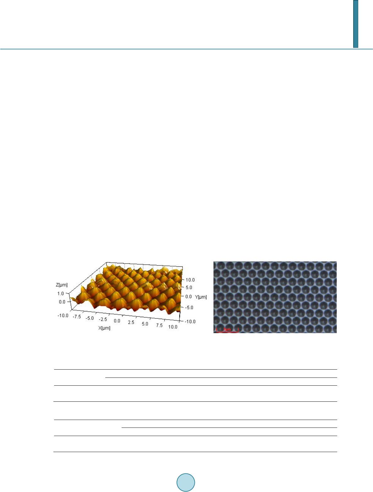
Journal of Applied Mathematics and Physics, 2014, 2, 1113-1117
Published Online November 2014 in SciRes. http://www.scirp.org/journal/jamp
http://dx.doi.org/10.4236/jamp.2014.212129
How to cite this paper: Adhikari, S., et al. (2014) Growth and Fabrication of GaN/InGaN Violet Light Emitting Diode on Pat-
terned Sapphire Substrate. Journal of Applied Mathematics and Physics, 2, 1113-1117.
http://dx.doi.org/10.4236/jamp.2014.212129
Growth and Fabrication of GaN/InGaN Violet
Light Emitting Diode on Patterned Sapphire
Substrate
Sonachand Adhikari1,2, Saroj Kanta Patra1,2, Ashok Lunia1, Sandeep Kumar1,
Priyavart Parjapat1, Bhoopendra Kushwaha1, Pawan Kumar1, Sumitra Singh1,
Ashok Chauhan1, Kuldip Singh1, Suchandan Pal1,2, C. Dhanavantri1,2
1CSIR-Network of Institutes for Solar Energy (CSIR-NISE), CSIR-Central Electronics Engineering Research
Institute (CSIR-CEERI), Pilani, Rajasthan, India
2Academy of Scientific and Innovative Research (AcSIR), Chennai, Tamil Nadu, India
Email: sonachand@ceeri.ernet.in
Received August 2014
Abstract
GaN/InGaN based violet light emitting diodes (LEDs), emitting at 430 nm, have been grown on
conventional single side polished (SSP) and patterned sapphire substrates (PSS). Characteristics
of the epitaxial wafers and subsequently fabricated LEDs have been analyzed. The photol umi nes-
cence (PL) peaks have been observed at 428.1 nm 426.1 nm for the epitaxial layers on SSP and PSS
respectively. The PL intensity is 2.9 times higher in the case of PSS. The electroluminescence (EL)
peaks have been observed at 430.78 nm and 430.35 nm for the LEDs on SSP and PSS respectively.
The light output from LED fabricated on the PSS is 2.15 times higher than that of the LED on SSP at
a forward current of 100 mA.
Keywords
LED, GaN/InGaN, PSS
1. Introduction
GaN is one of the most widely used direct band gap compound semiconductors with many optoelectronic appli-
cations. GaN and its related alloys are currently used extensively for the fabrication of light emitting diodes
(LEDs) and laser diodes (LDs). However, the main drawback for this material is the presence of a high thread-
ing dislocation density (TDD) due to the lattice mismatch between the sapphire substrate and the epitaxial GaN
layer. Growth of epitaxial GaN on free-standing GaN substrate would reduce the TDD; however, the GaN sub-
strates are much costly compared to the sapphire substrates. Another approach to alleviate this problem is the
growth of GaN by epitaxial-lateral overgrowth (ELOG) technique, which involves several steps of processing
the GaN wafer before the overgrowth. Growth of GaN on patterned sapphire substrate (PSS) is the simplest and
most cost effective method to reduce the TDD. In recent years, there has been a tremendous effort to increase
S. Adhikari et al.
1114
the performance of nitride based LEDs. One of the methods to improve the light output from LEDs is through
the growth of LEDs’ epitaxial structure on PSS [1]-[6]. Epitaxial structures grown on PSS also have the added
advantages of enhancement in the light extraction from LEDs by providing different escape angles to the light,
whi ch otherwise would have been trapped in the GaN LED.
We investigated the performance of LEDs grown by metal-organic chemical vapour deposition (MOCVD) on
single side polished (SSP) sapphire substrate and patterned sapphire substrate (PSS). The morphology of the
PSS was analyzed using atomic force microscopy (AFM) and optical microscopy. The epitaxial layers were
characterized by x-ray diffraction (XRD) in a PANalytical X’Pert MRD Pro and photoluminescence (PL) mea-
surement was conducted in Accent RPM2000. Subsequently, violet GaN/InGaN based LEDs (emitting at the
wavelength of 430 nm) have been fabricated and their electrical and optical properties have been analyzed.
2. Experimental Methods
2.1. Growth of Epitaxial Structure
The epitaxial structure of the LED was grown on the SSP and PSS simultaneously in a Thomas Swan 3 × 2 CCS
MOCVD. NH3 was used as the source of N; TMGa, TMIn, TMAl and Cp2Mg were used as the sources of Ga, In,
Al and Mg respectively. 1% SiH4 in hydrogen was used for the n-type doping. The structure consists of 30 nm
thick nucleation layer, 3 µm thick undoped GaN followed by 1µm thick n-type GaN with a carrier concentration
of ~6 × 1018 cm3. The active region consists of 3 nm thick five quantum wells of InGaN separated by 10 nm
thick GaN barriers. 15 nm thick Al0.15Ga0.85N was employed as an electron blocking layer followed by a 120 nm
thick p-GaN layer with a carrier concentration of ~5 × 1017 cm3.
2.2. Fabrication of LED
LEDs were fabricated from the epitaxial structures grown on SSP and PSS. The fabrication steps involve pat-
terning by lithography and subjecting to Cl2/BCl3 reactive ion etching to a depth of 600 nm to form a mesa.
Pre-metallization etch for the n-type contact was carried out in buffer-oxide etchant for 1 minute. Ti/Al/Ni/Au
(20 nm/150 nm/40 nm/50 nm) was deposited using electron beam evaporation followed by lift-off and rapid
thermal annealing at 850˚C for 30 sec to form Ohmic contact to the n-type GaN. Pt/Ni/Au (3 nm/3 nm/4 nm)
was deposited and rapid thermal annealed at 550˚C for 300 sec in N2 ambient to form the transparent current
spreading layer. Ni/Au (20 nm/ 100 nm) were deposited upon the current spreading layer and annealed at 550˚C
for 300 sec to form the contacts to p-GaN.
3. Results and Discussion
The morphology of the PSS was analysed by AFM and optical microscopy. The PSS consists of conical
protrusions with a pattern height of ~500 nm, a periodicity of 3 µm having a basal diameter of 2 µm. The AFM
and optical images of the PSS is shown in Figur e 1.
XRD measurement for the epitaxial layers grown on both SSP and PSS were carried out in symmetric (002)
and asymmetric (102) planes for the estimation of TDD through broadening of XRD curves. The symetric (002)
peak is broadened by screw dislocation
screw
N
, which can be calculated as suggested by [7]
( )
( )
( )
22
screw screw
002
FWHM 9Nb=
(1)
where
screw
b
is the Burgers vector corresponding to screw dislocation
( )
screw
0.5185 nmb=
. Edge dislocation
density
edge
N
have been estimated from the asymmetric (102) scan of of the epitaxial layers. The
edge
N
has
been calculated as
( )
( )
( )
22
edge edge
102
FWHM 9Nb=
(2)
where
edge
b
is the Burgers vector corresponding to edge dislocation
. Therefore, the total
dislocation density
total
N
can be calculated as
totalscrew edge
NN N= +
(3)
The above calculations are summarized in Table 1. The
total
N
of the PSS (6.25 × 108 cm2) is lower than that
S. Adhikari et al.
1115
of SSP (7.92 × 108 cm2).
The photoluminescence (PL) measurement of the LED structure on both SSP and PSS were carried out and
their PL emission patterns are shown in Figure 2. The peak wavelengths of SSP and PSS epitaxial LED
structures were observed at 428.1 nm and 426.1 nm respectively. The PL intensity from the PSS is 2.9 times
compared to that of the SSP under the same measurement conditions, which qualitatively indicates a much better
epitaxial layer structure in the case of PSS.
Electroluminescence (EL) measurements were carried out after the fabrication of LEDs at a current of 100
mA. The EL spectra for the LEDs fabricated on SSP and PSS substrates is shown in Figure 3. The EL spectra
closely follows their respective PL spectra. EL intensity of the LED on PSS is 2.7 times higher compared to that
on the SSP, which is due to the enahncement in extration of light because of the underlying PSS.
Specific Contact resistance of Ti/Al/ Ni/Au on n-GaN and Ni/Au on p-GaN were measured through the trans-
fer length method (TLM) for both SSP and PSS samples and are summarized in Table 2. The resistance of the
samples were obtained by sweeping the voltage from −2 to +2 V and measuring the current. I-V characteristics
were linear, which meant that the contacts to both n-GaN and p-GaN were Ohmic in nature. The contact resis-
tance was of the order of few Ωs for n-GaN and few kΩs for p-GaN layer respectively.
I-V and L-I characteristics of the fabricated LED samples on SSP and PSS are plotted in Figure 4. It is evi-
dent that the LEDs fabricated on PSS have higher light output power as compared to those of the LEDs fabri-
cated on SSP. At a current of 100 mA, the light output from the LEDs on PSS was 2.15 times higher than the
LEDs on SSP. The above result is due to the fact that micro-pattering of sapphire substrate provides different
escape angles to light which results in higher light extraction efficiency.
4. Conclusion
Violet emitting GaN/InGaN based epitaxial structures of LED have been grown in MOCVD on SSP and PSS.
The TDDs on the SSP and PSS have been evaluated by XRD and it is observed that the TDDs have been re-
duced in the epitaxial layers grown on PSS. The PL emission intensity of the LED structure on PSS is 2.9 time-
shigher compared to the one on SSP, which infers better epitaxial layer on the PSS. The EL and L-I characteris-
(a) (b )
Figure 1. (a) AFM image of the PSS; (b) Optical microscopy image of the PSS.
Table 1. Summary of the Nscrew, Nedge and Ntotal determined from the XRD measurement.
Samp le FWHM (arcsec) Dislocation Density (cm
−2
)
(002)
(102)
N
Screw
N
Edge
N
Total
SSP 256 533 6.39 × 10⁷ 7.29 × 10⁸ 7.92 × 10⁸
PSS 283 462 7.76 × 10
7
5.48 × 10
8
6.25 × 10
8
Table 2. Specific contact resistance measurement on both n-contact and p-contact for SSP and PSS.
Samp le Specific contact resistance (Ωcm
2
)
N-Type P-Type
SSP 7.84 × 10
−5
1.28 × 10
−2
PSS
4.77 × 10⁻⁵
2.89 × 10⁻²
S. Adhikari et al.
1116
Figure 2. PL spectra of LED epitaxial structures on SSP and PSS.
Figure 3. EL spectra of LED epitaxial structures on SSP and PSS.
Figure 4. L-I and I-V characteristics of the LEDs on SSP and PSS.
tics confirm the enhancement of light extraction in the case of PSS. The light output at 100 mA is 2.15 times in
the case of PSS.
Acknowledgem ents
Authors are thankful to the director, CSIR-CEERI-Pilani for his encouragement and constant support. Authors
S. Adhikari et al.
1117
also acknowledge the CSIR for funding TAPSUN programme by sponsoring NWP-55 project.
References
[1] Tadato mo, K., Okaga wa, H., Ohuchi , Y., Tsunekawa, T., Jyouichi, T., Ima da , Y., et al. (2001) High Output Power In-
GaN Ultraviolet Light-Emitting Diodes Fabricated on Patterned Substrates Using Metalorganic Vapor Phase Epitaxy.
Physica Status Solidi (a), 188, 121-125.
http://dx.doi.org/10.1002/1521-396X(200111)188:1<121::AID-PSSA121>3.0.CO;2-G
[2] Chang, S.J., Li n, Y.C., Su , Y.K., Chang, C.S., Wen, T.C ., Shei , S.C., et al. (2003) Nitride-Based LEDs Fabricated on
Patterned Sapphire Substrates. Solid -State Electronics, 47, 1539-1542.
http://dx.doi.org/10.1016/S0038-1101(03)00073-X
[3] Fe ng, Z.H., Qi, Y.D., Lu, Z.D. and Lau, K.M. (2004) GaN -Based Blue Light-Emitting Diodes Grown and Fabricated
on Patterned Sapphire Substrates by Metalorganic Vapor-Phase Epitaxy. Journal of Crystal Growth, 272, 327-332 .
http://dx.doi.org/10.1016/j.jcrysgro.2004.08.070
[4] Kao, C.-C., Su, Y.-K., Hsieh, Y.-T., Lee, Y.-C., Cheng, C.-Y. and Lin, C.-L. (20 11 ) Investigation of GaN-Based
Ligh t -Emitting Diodes Grown on Patterned Sapphire Substrates by Contact-Transferred and Mask-Embedded Litho-
graphy. Applied Physics Express, 4, 062102-06 2104 . http://dx.doi.org/10.1143/APEX.4.062102
[5] Ya mada, M., Mitani, T., Narukawa, Y., Sh ioji, S., Niki, I., Sonobe, S., et al. (2002 ) I nGaN -Based Near-Ultraviolet and
Blue-Ligh t -Emitting Diodes with High External Quantum Efficiency Using a Patterned Sapphire Substrate and a Mesh
Electro de. Japanese Journal of Applied Physics, 41, L1431-L1433. http://dx.doi.org/10.1143/JJAP.41.L1431
[6] Yu, S.-F., Chang, S.-P., Chang, S.-J., Lin, R.-M., Wu, H.-H. and Hsu, W.-C. (2012) Characteristics of InGaN-Based
Ligh t -Emitting Diodes on Patterned Sapphire Substrates with Various Pattern Heights. Journal of Nanomaterials, 2012.
http://dx.doi.org/10.1155/2012/346915
[7] Mo ram, M.A. and Vi ckers, M.E. (2009) X-Ray Diffraction of III-Nitrides. Reports on Progress in Physics, 72, Article
ID: 036502. http://dx.doi.org/10.1088/0034-4885/ 72/ 3/03 6502