Materials Sciences and Applications
Vol.4 No.1(2013), Article ID:27068,10 pages DOI:10.4236/msa.2013.41005
Improved Low-Temperature Aqueous Synthesis of ZnO Nanorods and Their Use in SERS Detection of 4-ABT and RDX
![]()
1Department of Chemistry, University of Puerto Rico-Mayaguez, Mayagüez, Puerto Rico; 2Department of Engineering Science and Materials, University of Puerto Rico-Mayaguez, Mayagüez, Puerto Rico; 3Department of Chemistry, University of North Florida, Jacksonville, USA; 4Department of Chemistry and Physics, University of Puerto Rico-Ponce, Ponce, Puerto Rico.
Email: *samuel.hernandez3@upr.edu
Received September 21st, 2012; revised October 20th, 2012; accepted November 16th, 2012
Keywords: ZnO Nanorods; Sputtering; SERS; 4-ABT, RDX
ABSTRACT
The growth-controlled synthesis of zinc oxide nanorods (ZnO NR) in the aqueous phase has been investigated. The rods were grown on ZnO films previously deposited onto Si(100) and indium tin oxide (ITO) substrates by RF magnetron sputtering. The formation of the rods took place in the presence of hexamethylenetetramine (HMT) as habit-control reagent. The grains in the base ZnO film acted as seeds that promoted the longitudinal growth of the oxide. As-synthesized base films and rods were characterized by X-ray diffraction, scanning electron microscopy (SEM), field emission SEM, optical absorption and photoluminescence spectroscopy techniques. Subsequently, a wet chemistry procedure was performed to achieve ZnO NR growth. This methodology was conducive to the formation of rods of a relatively narrow distribution of diameters (60 - 70 nm) with lengths in the 1 - 3 μm range. Photoluminescence spectra were characterized by a dominant near-band-edge (NBE) peak followed by a green luminescence (GL) broad band, indicative of higher oxygen vacancy concentration in the ZnO NR grown on ZnO/ITO in comparison with those grown on ZnO/Si(100). A UV process was used for coating the ZnO NR with gold (Au). Au coating on ZnO NR was used to evaluate the detection capability by SERS of different analytes such as: 4-aminobenzenethiol (4-ABT) and 1,3,5-trinitroperhydro-1,3,5- triazine (RDX) at low levels. A strong SERS Raman spectrum was observed for 4-ABT. A limit of detection (LOD) of 1 × 10⁻⁸ M for 4-ABT was achieved corresponding to a minimum of 5.4 × 10⁵ molecules detected under the experimental conditions at excitation wavelength of 785 nm with a sensitivity of the ZnO NR in the range of 1.1 × 10⁻¹⁶ g under the laser spot.
1. Introduction
Recent developments in nanotechnology, along with the demonstration of various quantum size effects in nanoscale particles have been reported for zinc oxide (ZnO) with a special interest for rods and rod-like shapes. This morphology is of particular relevance for applications in chemical sensing, micro-lasers, cantilevers, optoelectronics and surface enhanced Raman spectroscopy (SERS)- based biosensors, among other device applications [1-6]. Studies on ZnO rods have demonstrated outstanding optical properties, when compared with spherical particles. ZnO rods favor the enhancement of the local field at the emitting surface with the subsequent drop in the turn-on electric field [7]. These optical features are dependent on the elongated morphologies and crystalline structure [2]which are critical to the design of multifunctional ZnO structures. The control on the shape of the ZnO product can be attained by careful manipulation of the synthetic method parameters such as reagent concentration, reaction time and temperature employed for its preparation [3]. Regarding the synthesis of ZnO nanostructures, various methods have been suggested, including vapor phase synthesis, low-temperature thermal deposition and high-temperature vapor phase transport (VPT) [8-10]. In particular, the formation of ZnO rods by hydrothermal growth, chemical bath deposition (CBD), electrophoresis and template-assisted growth, have been reported [11,12]. The hydrothermal synthesis process is commonly used for the preparation of ZnO rods and involves an epitaxial anisotropic crystal growth in a solution at low temperature [13-15].
Vayssieres reported on a method for fabrication of ZnO rods and nanowires in aqueous phase [16]. This route allows for the formation of well-crystallized rodshaped structures of better uniformity with respect to the samples produced via sol-gel methods [17-19]. Vayssieres’ original route was based on the thermal decomposition of zinc nitrate hexahydrate and methenamine solutions. This approach allowed the formation of wellaligned hexagonal ZnO rods, 100 - 200 nm wide and up to 10 µm long [14,20]. However, the study was limited to ZnO rods deposited onto a base film of ITO, without providing further details about the synthesis and characterization of the produced materials. Recently, a modification of Vayssieres’ method has been successfully applied by the authors for the preparation of a biosensor for urea [21]. Consequently, the present work is focused on the systematic study of the growth of ZnO NR and its dependence on the type of substrate and the sputtering conditions to deposit the ZnO base layer. The approach is relatively simple and easy-to-scale up and considers the use of a reflux system at 95˚C. Two types of substrate were evaluated: Si(100) and indium tin oxide (ITO), to determine whether their structural features affect the morphology of the rods obtained. However, lattice mismatches between the ZnO thin film deposited and the substrates could have a marked effect on the crystallinity of the rods produced. The mismatch is larger for ZnO base film on Si substrate than for ZnO base film on ITO substrate. An estimated lattice-mismatch difference of 40% between Wurtzite ZnO and cubic Si(100) is much harder to cope with than that for zinc oxide on ITO substrate which should exhibit a better crystal quality due to a small estimated lattice-mismatch of about 3% [22].
In addition, our work also focused on the evaluation of alternatives conducive to a more precise control of the rod thickness by proper selection of the deposition conditions for base ZnO films. It was expected that the finer the grain size in the base ZnO films, the thinner the ZnO NR that could be formed [14,17,20].
The activation of ZnO NR was usually carried out using the conventional optical method which employs a short-wave UV light lamp. This procedure is based on the photoreduction of gold (III) chloride hydrate (HAuCl4) in solution. Combining Au with ZnO semiconductor resulted in new stable substrates for SERS studies in the successful detection of analytes such as: 1,3,5-trinitroperhydro-1,3,5-triazine (RDX) and 4-aminoben-zenethiol (4-ABT) at low detection levels.
2. Experimental
2.1. Reagents
All reagents used were of analytical grade. The sputtering target used for the deposition of the base films consisted of zinc oxide (99.99% purity, 0.15" thick and 2" diameter) produced by Superconductor Materials, Inc. The p-type Si(100) and indium tin oxide (ITO; 15 - 25 Ω/in2) substrates were purchased from Sigma Aldrich Chemical Co. (Milwaukee, WI), hexamethylenetetramine (HMT), 99.99%, and zinc nitrate hexahydrate (Zn (NO3)2∙6H2O) were purchased from Sigma-Aldrich and were used to synthesize and deposit ZnO rods onto the above-mentioned sputtered base films. Gold (III) chloride hydrate (99.999% trace metals basis) was obtained from Sigma-Aldrich Chemical Co during this research and used for the preparation Au-coated ZnO NR.
2.2. Synthesis of ZnO Base Films Substrate
We have previously reported the growth of ZnO rods onto ZnO/ITO base film substrates by wet chemistry following Vassiere’s protocol [16]. This material was utilized to develop an urea biosensor and demonstrated the proposed technique to be successful [21]. In this work we conducted a systematic study of the deposition of ZnO NR, exhibiting different thickness, on ZnO base films deposited over ITO and Si(100) substrates by magnetron sputtering.
ZnO base films were grown using an ATC Orion 8 Linear Magnetron Sputtering instrument (AJA International, Inc., North Scituate, MA) of on-axis configuration, using 150 W of RF power and a deposition time of 10 min. The optimum position on substrate holder of the substrates with respect to the target distance was 8.0 cm. The base film growth took place under an argon atmosphere at 1.0 × 10⁻³ Torr and 120˚C ± 2˚C. The temperature was measured using a thermocouple, which was in contact with the top plate of the substrate holder.
2.3. Synthesis of ZnO Rods
ZnO rods were synthesized from the thermal decomposition of zinc nitrate hexahydrate/hexamethylenetetramine (HMT) in aqueous phase [14,20,21]. The ZnO base/Si substrate and ZnO base/ITO substrates, deposited by RF magnetron sputtering, were immersed in a glass beaker containing Zn (NO3)2·6H2O and HMT at a concentration of 0.01 M. ZnO base films were placed vertically at the bottom of the glass vessels. The reacting solution in contact with the films was refluxed at 95˚C for 1.5 hr. At the end of the contact time, treated films were removed from the solution and thoroughly washed with high purity water (Milli-Q, 18.2 MΩ·cm) to remove any residual amino complex. All ZnO rods were dried at 200˚C for 10 min and then characterized.
2.4. Preparation of Au Coating on ZnO NR Analytes
A UV light lamp was used to obtain Au-coated ZnO NR in order to detect various analytes. The experimental procedure was carried out using short-wave UV light based on the photoreduction of gold (III) chloride hydrate (HAuCl4), from a 1 × 10⁻³ M solutions with high purity water (MilliQ 18.2 MΩ·cm). ZnO NR films of 1 cm × 1 cm were swamped in a beaker with 4.0 mL of HAuCl4 solution at pH 7.2, during 2 hours of reaction time under exposition to UV light. Afterwards, films were rinsed with high purity water and dried at 120˚C for 2 hours to be used as substrates for SERS.
2.5. Sample Preparation for Analysis by SERS
For SERS analysis, ZnO NR was characterized using 4-ABT as SERS probe molecule. An aliquot of 2 μL of a solution 1 × 10⁻⁸ M of the analyte in ethanol was prepared and the pH adjusted to 7.5 and mixed with 100 mL of 0.1 M sodium chloride (NaCl). This mixture was sonicated for a period of 15 min followed by filtration through a 0.5 μm mesh. SERS spectra were recorded at the same conditions for: 4-aminobenzenethiol (4-ABT) and 1,3,5-trinitroperhydro-1,3,5-triazine (RDX). Raman spectra for each mixture was recorded using 785 nm excitation wavelength in a Renishaw Raman Microspectrometer with a 10× magnification and 170 mW head power.
2.6. Materials Characterization
X-Ray diffraction (XRD) measurements were carried out in a Siemens D5000 XRD using the Cu-K α radiation (1.5405 Å). Scanning electron microscopy (SEM) analyses were conducted on a JEOL-JSM 6500 instrument and a Philips/FEI, XL30 s, FEG SEM/Phoenix EDAX. Optical absorption measurements of ZnO rods were carried out with a Beckman DU 800 UV-VIS spectrophotometer. Photoluminescence (PL) spectra were acquired at room temperature (RT) with an HORIBA Jobin/Yvon FluoroLog-3 spectrofluorimeter at an excitation wavelength of 350 nm.
3. Discussion and Results
3.1. Structural and Optical Characterization of ZnO Rods Deposited onto ZnO/ITO Substrates
The X-ray diffraction patterns corresponding to the ZnO/ ITO substrates and the ZnO deposited onto this base are shown on Figures 1(a) and (b), respectively. In both samples, the diffraction patterns clearly show the preferential growth along the (002) plane in the wurtzite structure of ZnO. However, some ZnO NR did not grow in the c vertical axis due to the weaker appearance of the (101) and (102) planes. This suggests the formation of wellorganized columnar structures along c-axis direction perpendicular to the substrate. The peak at 35.4˚ corresponds to the ITO substrate.
The broadening of the XRD peaks evidenced the nanocrystalline nature of the ZnO NR grown. The average crystallite size, estimated by the Scherrer’s equation, was about 26 nm. Although both XRD patterns evidenced the preferential growth in c-axis direction (intensities of the (002) peak), the later was shifted toward lower diffraction angles in the pattern with respect to the standard value at 2θ = 34.422˚ (ICDD Powder Diffraction File #36-1451), as shown in Table 1 and in Figure 1(a). This shift can be attributed to tensile stress in the ZnO film deposited by sputtering onto the ITO substrate. It is also apparent that for the (002) plane, there is a slight shift from the standard value (2q = 34.422˚) [23]. The diffraction peaks can be indexed to a Wurtzite hexagonal structure of the bulk ZnO crystal with lattice constants for a = 0.32 nm and c = 0.51 nm from the orientation plane (002).
Table 1 summarizes XRD results and estimated crystallite size for ZnO thin films on the ITO and Si substrates, and for ZnO NR on ITO, Si(100). Note that the strain is tensile between ZnO and ITO and is compressive between ZnO and Si.
Table 1. Lattice parameters of ZnO thin films deposited on different substrates.
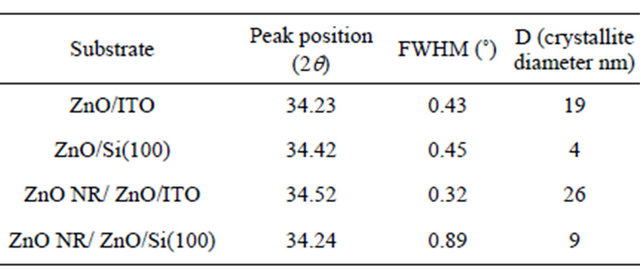

Figure 1. XRD patterns for: (a) ZnO base films deposited by sputtering on 15 - 25 Ω/in2 ITO substrates at 120˚C, and 10 min of deposition time; (b) ZnO/ITO base films with ZnO NR deposited.
Figure 2 shows the UV-VIS optical absorption spectrum for the ZnO rods grown on the ZnO/ITO substrate. The excitonic absorption peak is clearly observed about 364 nm, which exhibits a blue shift compared to bulk ZnO materials (388 nm) [24]. This blue shift observed may be attributed to a confinement of the ZnO rods to nanoscale dimensions [25]. Optical absorption analysis was not possible for the Si substrate due to the lack of transparency for the ZnO NR deposited on ZnO/Si(100) substrate in the UV-VIS spectral range of interest.
The photoluminescence spectra of ZnO NR deposited onto ZnO/ITO base films substrates are shown in Figure 3. The spectrum was recorded at room temperature and under an excitation wavelength of 350 nm. The spectrum clearly displays the dominant narrow near-band-edge (NBE) at 380 nm and also a weaker relative intensity a broad green luminescence (GL) at 550 nm emission band previously reported in ZnO thin films [25,28]. Even though the origin of the GL band has been a matter of discussion [26-28] it is typically associated with deeplevel defects such as oxygen vacancies and interstitial Zn ions, which is largely dependent on the synthetic route used for preparation of the ZnO NR.

Figure 2. UV-VIS spectrum of ZnO rods deposited onto ZnO/ITO base film.
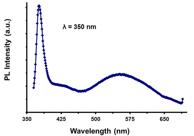
Figure 3. PL spectra for ZnO rods obtained at an excitation wavelength of 350 nm.
3.2. Structure and Characterization of ZnO Rods Deposited onto ZnO/Si(100) Substrates
Figure 4 shows the diffraction patterns of ZnO/Si(100) base film substrates (4a) and the corresponding ZnO rods deposit (4b). In this case, the base film was produced after a sputtering time of 10 min. The peak broadening observed in the XRD pattern of ZnO base film suggests indicates a smaller crystallite size, with respect to those presented in Section 3.1. The estimated average crystallite size using Scherrer’s formula was 9 nm, which is larger than the 4 nm estimated for the ZnO base film deposited onto ITO substrates. This is mainly due to different types of ZnO stress on these substrates. Also, in this case, the exclusive presence of the (002) diffraction peak evidences the preferential growth of (002) planes in both the ZnO base film and the ZnO deposit. Furthermore, the preferential growth of the (002) plane and the absence of other planes different from those corresponding to the (001) plane in the ZnO deposit confirm the strong out-of-plane orientation for ZnO NR/ZnO/Si. This suggests the development of columnar crystals.
Shown in Figure 5 are PL results obtained for ZnO rods grown on the ZnO base film/Si(100) substrates. The spectra were recorded at an excitation wavelength of 350 nm, which lies within the absorption profile of the nanostructures. A weak shoulder near 381 nm was observed and was attributed to donor acceptor pair levels in ZnO base on p-type Si(100) substrate [28].
A small blue shift was observed on ZnO NR/ZnO/Si with respect to ZnO NR/ZnO/ITO corroborates XRD results. Both Figures 3 and 5 clearly display the dominant narrow NBE and also the broad GL emission bands with lower relative intensity characteristic of ZnO rods [25,28], at 380 nm and 550 nm, respectively. As observed, the qualitative features of the ZnO NR spectra are similar in both surfaces, regardless of the nature of the
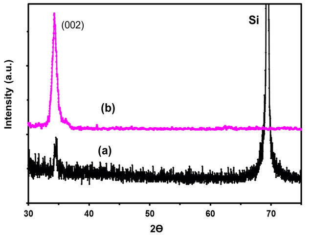
Figure 4. XRD patterns for: (a) ZnO/Si(100) base film deposited by sputtering at 120˚C and 12 min of deposition time; (b) ZnO rods deposited onto the ZnO/Si base film.
substrate, mainly due to the use of ZnO base thin films on those substrates. Moreover, the relative PL intensity ratios of the UV NBE emission to the GL band (IUV/Ivis) are 0.3 and 0.4 for the ZnO base film/ITO and ZnO base film/Si(100) substrates, respecttively. Thus, the similar IUV/Ivis ratios observed herein are indicative of the reliability of the preparation procedure for yielding ZnO NR in a consistent manner for both the ITO and Si(100) substrates. Regarding the ZnO/Si(100) and ITO base films, significant emission could not be recorded, due to the lack of nanostructure on base thin films.
3.3. Comparative Morphological Analyses for ZnO NR Deposited on ZnO/Si(100) and ZnO/ITO
In order to attain additional insights on the morphological features of our samples, prepared base films and ZnO deposits were analyzed by field-emission scanning electron microscopy.
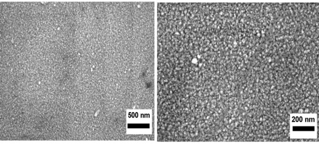
FE-SEM images shown in Figure 6 correspond to the ZnO/Si(100) base films grown by RF magnetron sputtering. The films appear highly compact, which suggest a good quality deposition. The grains look equiaxial. These grains are considered as seeds for the growth of the corresponding rods.
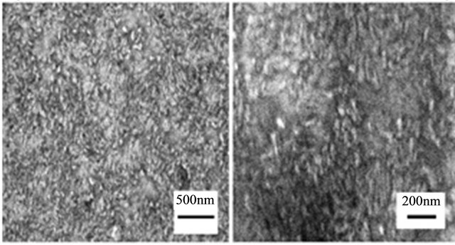
The FE-SEM images shown in Figure 7 correspond to the ZnO/ITO base film. As with the Si(100) substrate, the films also seem uniform and compact again suggesting
 (a)
(a)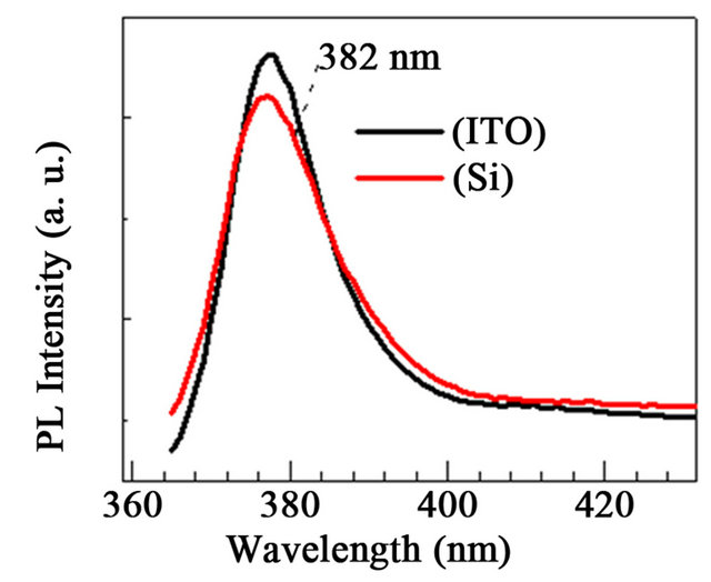 (b)
(b)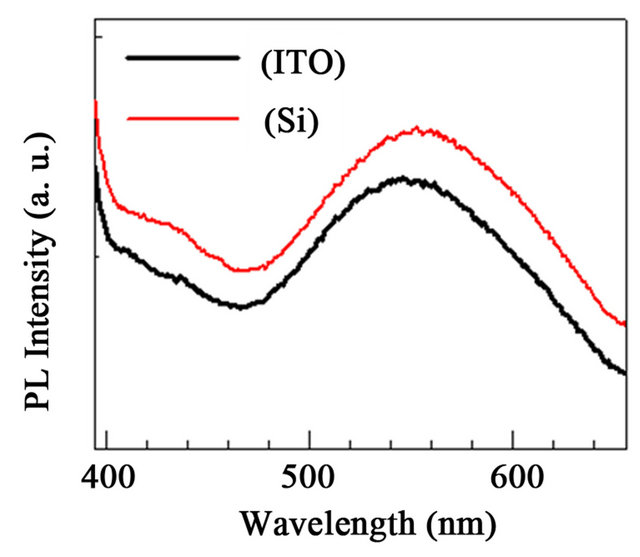 (c)
(c)
Figure 5. PL spectra for ZnO NR obtained at an excitation wavelength of 350 nm. (a) ZnO NR deposited onto ZnO/Si and ZnO/ITO base films; (b) Comparison of UV NBE emission band for ZnO NR deposited onto substrates. A weak shoulder is discernible at 382 nm; (c) GL band for ZnO NR deposited onto substrates.
 (a) (b)
Figure 6. FE-SEM images of the ZnO base film/Si(100) film deposited by RF magnetron sputtering for 10 min at 120˚C. Scale markers: (a) 500 nm; (b) 200 nm.
 (a) (b)
Figure 7. FE-SEM images of the ZnO base film/ITO film deposited by RF magnetron sputtering for 10 min at 120˚C. Scale markers: (a) 500 nm; (b) 200 nm.
good sputtering deposition quality. When comparing Figures 6 and 7, the morphological features in both types of ZnO base films are evident. While ZnO grains were more or less equiaxial when ZnO was deposited on Si(100), they exhibited elongated shape when ITO was used as substrate. The crystal growth on the Si(100) substrate is a function of a particular orientation of the Si atoms on a specific plane. The size of the structures varies by orders of magnitude, from nonporous silicon to mesoporous Si, with crystallites in the nanometer scale. The diverse morphological features of porous Si can be affected by pore orientation, filling of macropores and depth variation of porous Si [29]. However, ITO substrates do not have an orientation-specific plane and they typically have low roughness upon manufacture. These structural differences affect the morphology of ZnO base film deposited by RF magnetron sputter on Si(100) and ITO substrates.
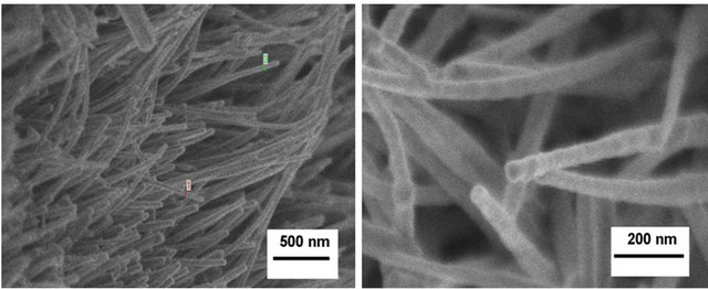
Figure 8 shows the FE-SEM images of the ZnO deposited on ZnO/Si(100), Figures 8(a) and (b) and ZnO/ ITO Figures 8(c) and (d) base films substrates. The rodshaped particles are clearly noted. Rods deposited onto ZnO/Si(100) base films averaged 60 nm in thickness with lengths above 3 μm. ZnO rods grown onto ZnO/ITO base films were also nanometric in thickness (~70 nm) although shorter (up to 500 nm in length) compared to the rods grown on ZnO/Si(100) base films. These small differences in morphology of the ZnO NR can be attributed to the observed differences on the morphology (grain size and shape) of the base films [30].
The appropriate selection of the synthesis conditions, such as temperature and concentration of the reactants in aqueous phase, allowed a certain degree of control on the crystal growth rate and the final morphology of the NR obtained. HMT plays a key role in the growth of rodshaped ZnO nanostructures contributing to form a 7.2 pH buffer. HMT would thermally decomposed to release OH− ions as required for the formation of intermediate Zn(OH)2 [12] and subsequent dehydration to form the corresponding oxide. Regarding particle shape, the preferential adsorption of amine groups (from HMT) on specific crystallographic planes of ZnO has been reported, promoting the preferential growth along the “c” axis of the hexagonal Wurtzite unit cell, which explains the rod-shaped morphology observed by FE-SEM analyses [31].
Compared to Vayssieres’ method, our approach favors formation of NR of thinner diameter (~60 nm) and shorter length (<3 mm) [16]. It has been observed that NR covered with a thin layer of gold of these dimensions exhibit SERS performance with the possibility of molecule-level detection of different analytes [6].
3.4. Structure and Characterization of Au Coated on ZnO Rods Deposited onto ZnO/Si(100) and ZnO/ITO Substrates
Diffraction patterns for ZnO NR/ZnO base film/ITO are
 (a)
(a) (b)
(b)
Figure 8. FE-SEM images of ZnO NR deposited onto: (a), (b) ZnO/Si(100); (c), (d) ZnO/ITO base film; (d) ZnO/ITO, base film. Scale markers (a), (c) 500 nm; (b), (d) 200 nm.
shown in Figure 9(a). The three orientation planes (100) for ZnO and (111) and (200) for Au structures are observed. The (002) plane is absent, suggesting deformation of columnar structures along the c-axis in a direction perpendicular to the substrate for ZnO NR. Usually the (002) plane corresponds to a maximum intensity of ZnO zincite Wurtzite structure.
The broadening of the XRD peak evidenced the nanocrystalline nature of the ZnO deposit. The average crystallite size, estimated by the Scherrer’s equation, was around 4.0 nm. Au-coated on ZnO NR/ZnO base film/ Si(100) shows a rise with respect to the (111) plane and signals also appear for the (200) and (220) planes characteristic of the fcc Au phase [32,33], as can be observed on Figure 9(b). Reduction of the (002) planes with respect to (111), confirmed the deposition of Au on ZnO NR. Wamng et al. [34] have studied the electron transfer of the ZnO/Au system under UV light and concluded that the electrons transfer from Au to ZnO to form a uniform Fermi energy level during the formation of the Au-ZnO junction, as gold has a higher Fermi energy level than ZnO. Transferred electrons accumulate on the equilibrated Fermi level near the bottom of the conduction band of ZnO. Thus, more electrons can drop from the conducting band of ZnO to the valence band and recombine with holes, so more photons are radiated.
3.5. Surface Enhanced Raman Spectroscopy
Figure 10 shows the Raman spectrum for Au-coated ZnO NR/ZnO base film/Si(100) at 785 nm. The NR was active for in this excitation line. The band at 521 cm−1 is attributed to the silicon surface signal. A broad peak appears from 1500 up to 3000 cm−1, from photoluminescence due to the gold coating.
4-ABT was selected as SERS probe molecule because

Figure 9. XRD (a) Au-coated on ZnO NR/ZnO base film/ ITO and (b) Au-coated on ZnO NR/ZnO base film/Si(100). Au coating on ZnO NR were formed by the reaction 1 × 10⁻³ M of HAuCl4 aqueous solution kept at pH 7.2, with 2 hours of UV-irradiation reaction time at room temperature.
it absorbs strongly on gold from a gold-sulfate bond [34] activity of the ZnO NR. Figure 11 shows SERS of 4-ABT on Au coating ZnO NR/ZnO base film/Si obtained by both methods, ion beam sputtering and UV light lamp irradiation. A peak at 390 cm−1 confirms that 4-ABT molecules are bound via a gold-sulfate bond. The Au-S mode increased in intensity with concentration from 1 × 10⁻⁸ M up to 1 × 10⁻⁴ M of 4-ABT. This last result indicates that 4-ABT was oriented perpendicular to the Au-coated ZnO NR surface [33]. The enhancement of intensities of the peaks correspond to: C-S stretching (1075), C-H stretching (1171), C-H bend and C-C bending (1374) and the C-C stretching 1588 cm−1 [34]. These are mainly due to the field enhancement effect induced by surface plasmon polaritons of Au-coated ZnO NR [1].
Strong SERS of Raman spectra was observed for 4-ABT. However the experiments were realized with addition of Cl− ions to increase the ionic strength effect. A limit of detection (LOD) of 1 ×10⁻⁸ M for ABT was

Figure 10. Raman spectrum of Au-coated on ZnO rods deposited onto base film on Si(100).
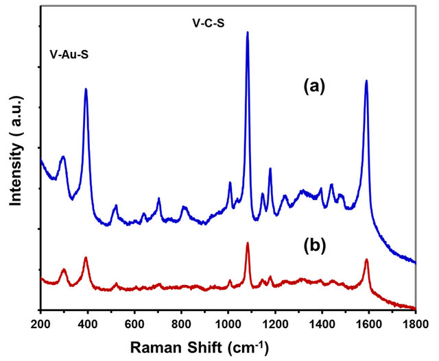
Figure 11. SERS of 4-ABT Au coating ZnO NR/ZnO base film/Si UV light lamp (a) 5.4 × 10⁹ molecules/cm2 of 4-ABT (b) 5.4 × 10⁵ molecules/cm2 of 4-ABT on Au-ZnO NR.
achieved corresponding to a minimum of 5.4 × 10⁵ molecules/cm2 detected under the experimental conditions at excitation wavelength of 785 nm with a sensitiveity of the ZnO NR in the range of 1.1 ×10⁻¹⁶ g under laser spot, with a SEF of 7.5 × 10⁸. The enhancement signal was induced by the chemical effect, due to an electronic resonance transfer between absorbed molecules and the metal surface [35]. The contribution of chemical enhancement is in the order of 101 to 102. Therefore the electromagnetic factor can be attributed to 106 up to 1014. Both effects contribute to high SERS enhancements factors for Au-ZnO NR [36].
Figure 12 shows SERS spectra at different concentrations of RDX on Au-coated ZnO NR/ZnO base film/Si (100). The development of this method allowed for lowering of the detection limit of RDX in thin films. A similar procedure was used in both samples dissolved in ethanol prepared at an adjusted pH = 7.5 and mixed with 100 mL of 0.1 M sodium chloride (NaCl). Acquisitions were obtained at 3 accumulation, 10 s integration time using a laser power of 785.0 nm, 98 mW measured at head.
The 874 cm−1 peak diminished in ISERS to a concentration of 1 × 10⁻⁴ in comparison with the concentration of 1 × 10⁻⁶ M of RDX components. Low detection limits were found for this analyte (9 × 10⁻¹⁹ g under spot of laser).
Raman-bands assignments of RDX are as follows: the vibration mode at 930 cm−1 is assigned to ring stretching and NO deformation signal intensity in SERS. The band at 874 cm−1 is attributed to the symmetric ring-breathing mode; the band at 1258 cm−1 is due to CH2 scissoring and N-N stretch vibration; [37] the band at 1312 cm−1 results from CH2 wagging; the band at 1370 cm−1 is υ NO2 symmetric stretching vibration and β CH2 scissoring. Finally the band at 1560 cm−1 is attributed to the υ NO2 asymmetric stretch in nitramines [37].
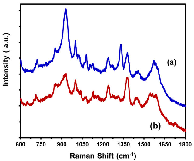
Figure 12. SERS of RDX on Au coating ZnO NR/ZnO base film/Si UV light lamp method. (a) 5.4 × 10⁹ molecules/cm2 of RDX (b) 5.4 × 10⁷ molecules/cm2 of RDX.
4. Conclusions
ZnO NR were successfully synthesized by a simple, lowtemperature aqueous processing route based on thermal decomposition of Zn precursors in the presence of HMT using a base film substrate for attaching the prepared NR. The selection of appropriate substrates, Si(100) or ITO, and sputtering conditions led to the formation of compact, uniform and submicrometric grain size ZnO base films. The observed differences in thickness and length of as-synthesized ZnO NR were attributed to the morphological features of the base films. As-synthesized ZnO NR exhibit Wurtzite structure and good optical behavior as suggested by UV-VIS and photoluminescence measurements. Produced nanorods will be explored in the fabrication of chemical sensors, such as surface enhanced Raman spectroscopy (SERS).
The Au coated ZnO NR/ZnO base film/Si(100) present are associated with higher stability in reference to their size with respect to Au coated ZnO NR/ZnO base film/ITO. These were obtained after 2 hours under experimental conditions with UV light. These ZnO NR were reproducible, when these were used as SERS sensors. 4-ABT was selected as SERS probe molecule because it absorbs strongly on gold. A limit of detection (LOD) of 1 × 10⁻⁸ M for ABT was achieved corresponding to a minimum of 5.4 × 10⁵ molecules detected under the experimental conditions at excitation wavelength of 785 nm with a sensitivity of the ZnO NR in the range of 1.1 × 10⁻¹⁶ g under laser spot, with a SEF of 7.54 × 10⁸. The enhancement signal was induced by the chemical effect, due to an electronic resonance transfer between the absorbed molecules and the metal surface.
On the other hand, a low detection limit of 9 × 10⁻¹⁹ g under spot of laser was found for RDX. This limit of detection was achieved by adjusting the pH and addition of Cl− ions to increase the ionic strength effect, which induces electrostatic charge changes on the Au coated ZNO NR surface.
5. Acknowledgements
Support from the U.S. Department of Homeland Security under Award Number 2008-ST-061-ED0001 is also acknowledged. However, the views and conclusions contained in this document are those of the authors and should not be considered a representation of the official policies, either expressed or implied, of the US Department of Homeland Security.
This contribution was supported by the U.S. Department of Defense, Proposal Number: 58949-PH-REP, Agreement Number: W911NF-11-1-0152. The authors also acknowledge contributions from Dr. Richard T. Hammond from Army Research Office, DOD. M. Balaguera would like to express her gratitude to J. Ortega and G. Cruz from Chemical Lab of Hewlett Packard-PR for facilitating the FE-SEM images and B. Renteria from NANO-Materials Processing Lab for XRD spectra. J. A. Jiménez thanks M. Sendova for the photoluminescence spectra at Optical Spectroscopy and Nano-Materials Lab at New College of Florida, Sarasota, FL.
REFERENCES
- X. Hu, Y. Masuda, T. Ohji and K. Kato, “Control of Crystal Growth for ZnO Nanowhisker Films in Aqueous Solution,” Thin Solid Films, Vol. 518, No. 2, 2009, pp. 906-910. doi:10.1016/j.tsf.2009.07.114
- J. Liu, Z. Guo, F. Meng, Y. Jia, T. Luo, M. Li and J. Liu, “Novel Single-Crystalline Hierarchical Structured ZnO Nanorods Fabricated via a Wet-Chemical Route: Combined High Gas Sensing Performance with Enhanced Optical Properties,” Crystal Growth & Design, Vol. 9, No. 4, 2009, pp. 1716-1722. doi:10.1021/cg8006298
- M. Huang, M. Mao, H. Feick, Y. Yan, W. Kind, E. Weber, R. Russo and P. Yang, “Room-Temperature Ultraviolet Nanowire Nanolasers,” Science, Vol. 292, No. 5523, 2001, pp. 1897-1899. doi:10.1126/science.1060367
- D. C. Reynolds, D. C. Look, B. Jogai, C. W. Litton, T. C. Collins, W. Harsch and G. Cantwell, “Neutral-DonorBound-Exciton Complexes in ZnO Crystals,” Physical Review B, Vol. 57, No. 19, 1998, pp. 12151-12155.
- X. Wang, X. Kong, Y. Yu and H. Zhang, “Synthesis and Characterization of Water-Soluble and Bifunctional ZnOAu Nanocomposites,” The Journal of Physical Chemistry C, Vol. 111, No. 10, 2007, pp. 3836-3841. doi:10.1021/jp064118z
- J. L. Chen, L. Luo, Z. Chen, M. Zhang, J. A. Zapien, C. S. Lee and S. T. Lee, “ZnO/Au Composite Nanoarrays As Substrates for Surface-Enhanced Raman Scattering Detection,” The Journal of Physical Chemistry C, Vol. 114, No. 1, 2010, pp. 93-100. doi:10.1021/jp908423v
- A. Dev, S. A. Panda, S. Kar, S. Chakrabarti and S. Chaudhuri, “Surfactant-Assisted Route to Synthesize WellAligned ZnO Nanorod Arrays on Sol-Gel-Derived ZnO Thin Films,” The Journal of Physical Chemistry B, Vol. 110, No. 29, 2006, pp. 14266-14272. doi:10.1021/jp062729l
- Y. Xia, P. Yang, Y. Sun, Y. Wu, B. Mayers, B. Gates, Y. Yin, F. Kim and H. Yan, “One-Dimensional Nanostructures: Synthesis, Characterization, and Applications,” Advanced Materials, Vol. 15, No. 5, 2003, pp. 353-389. doi:10.1002/adma.200390087
- L. Liao, H. B. Lu, J. C. Li, H. He, D. F. Wang, D. J. Fu and C. Liu, “Size Dependence of Gas Sensitivity of ZnO Nanorods,” The Journal of Physical Chemistry C, Vol. 111, No. 5, 2007, pp. 1900-1903. doi:10.1021/jp065963k
- D. J. Park, D. C. Kim, J. Y. Lee and H. K. Cho, “Synthesis and Microstructural Characterization of the Growth Direction Controlled ZnO Nanorods Using a Buffer Layer,” Nanotechnology, Vol. 17, No. 20, 2006, pp. 5238-5243. doi:10.1088/0957-4484/17/20/032
- L. E. Greene, M. Law, D. H. Tan, M. Montano, J. Goldberger, G. Somorjai and P. D. Yang, “General Route to Vertical ZnO Nanowire Arrays Using Textured ZnO Seeds,” Nano Letter, Vol. 5, No. 7, 2005, pp. 1231-1236. doi:10.1021/nl050788p
- Y. C. Wang, I. C. Leu and M. H. Hon, “Preparation Andcharacterization of Nanosized Zno Arrays by Electrophoretic Deposition,” Journal of Crystal Growth, Vol. 237- 239, Pt. 1, 2002, pp. 564-569. doi:10.1016/S0022-0248(01)01984-4
- K. Govender, D. S. Boyle, P. B. Kenway and P. O’Brien, “Understanding the Factors that Govern the Deposition and Morphology of Thin Films of ZnO from Aqueous Solution,” Journal of Materials Chemistry, Vol. 14, No. 16, 2004, pp. 2575-2591. doi:10.1039/b404784b
- R. C. Wang, L. H. Ying, C. H. Shu, L. Y. Feng and R. S. Huang, “Boundary Layer-Assisted Chemical Bath Deposition of Well-Aligned ZnO Rods on Si by a One-Step Method,” Applied Physics A, Vol. 96, No. 3, 2009, pp. 775-781. doi:10.1007/s00339-009-5271-6
- D. Byrne, E. McGlynn, K. Kumar, M. Biswas, M. O. Henry and G. Hughes, “A Study of Drop-Coated and Chemical Bath-Deposited Buffer Layers for Vapor Phase Deposition of Large Area, Aligned, Zinc Oxide Nanorod Arrays,” Crystal Growth & Design, Vol. 11, No. 12, 2011, p. 400.
- L. Vayssieres, et al., “Purpose-Built Anisotropic Metal Oxide Material: 3D Highly Oriented Microrod Array of ZnO,” The Journal of Physical Chemistry B, Vol. 105, No. 17, 2001, pp. 3350-3352. doi:10.1021/jp010026s
- J. S. Na, B. Gong, G. Scarel and G. N. Parsons, “Surface Polarity Shielding and Hierarchical ZnO Nano-Architectures Produced Using Sequential Hydrothermal Crystal Synthesis and Thin Film Atomic Layer Deposition,” ACS Nano, Vol. 10, No. 10, 2009, pp. 3191-3199. doi:10.1021/nn900702e
- C. D. Bojorge, V. R. Kent, E. Teliz, H. R. Cánepa, R. Henríquez, H. Gómez, R. E. Marotti and E. A. Dalchiele, “Zinc-Oxide Nanowires Electrochemically Grown onto Sol-Gel Spin-Coated Seed Layers,” Physica Status Solidi A, Vol. 208, No. 7, 2011, pp. 1662-1669. doi:10.1002/pssa.201026752
- D. Wan, F. Huang and Y. Wang, “Highly Surface-Textured ZnO: Al Films Fabricated by Controlling the Nucleation and Growth Separately for Solar Cell Applications,” ACS Applied Materials & Interfaces, Vol. 2, No. 7, 2010, pp. 2147-2152. doi:10.1021/am100416e
- L. Vayssieres, N. Beermann. S. E. Lindquist and A. Hagfeldt, “Controlled Aqueous Chemical Growth of Oriented Three-Dimensional Crystalline Nanorod Arrays: Application to Iron(III) Oxides,” Chemistry of Materials, Vol. 13, No. 2, 2001, pp. 233-235. doi:10.1021/cm001202x
- N. Palomera, M. Balaguera, S. K. Arya, S. P. Hernández, M. S. Tomar, J. E. Ramírez and S. P. Singh, “Zinc Oxide Nanorods Modified Indium Tin Oxide Surface for Amperometric Urea Biosensor,” Journal of Nanoscience and Nanotechnology, Vol. 11, No. 8, 2011, pp. 6683-6689. doi:10.1166/jnn.2011.4248
- Z. J. Wang, H. M. Zhang, L. G. Zhang and J. S. Yuan, “Structure and Strong Ultraviolet Emission Characterist Ics of Amorphous ZnO Films Grown by Electrophoretic Deposition,” Journal of Materials Research, Vol. 18, No. 1, 2003, pp. 151-155. doi:10.1557/JMR.2003.0021
- X. Gao, X. Li and W. Yu, “Flowerlike ZnO Nanostructures via Hexamethylenetetramine-Assisted Thermolysis of Zinc-Ethylenediamine Complex,” The Journal of Physical Chemistry B, Vol. 109, No. 3, 2005, pp. 1155-1161. doi:10.1021/jp046267s
- N. S. Pesika, K. J. Stebe and P. C. Searson, “Relationship between Absorbance Spectra and Particle Size Distributions of Quantum Sized Nanocrystals,” The Journal of Physical Chemistry B, Vol. 107, No. 38, 2003, pp. 10412- 10415. doi:10.1021/jp0303218
- L. Yanhong, W. Dejun, Z. Qidong, Y. Min and Z. Qinglin, “A Study of Quantum Confinement Properties of Photogenerated Charges in ZnO Nanoparticles by Surface Photovoltage Spectroscopy,” The Journal of Physical Chemistry B, Vol. 108, No. 10, 2004, pp. 3202-3206. doi:10.1021/jp037201k
- X. Liu, X. Wu, H. Cao and R. P. Chang, “Growth Mechanism and Properties of ZnO Nanorods Synthesized by Plasma-Enhanced Chemical Vapor Deposition,” Journal of Applied Physics, Vol. 95, No. 6, 2004, pp. 3141-3147. doi:10.1063/1.1646440
- D. Wang, H. W. Seo, C. C. Tin, M. J. Bozack, J. R. Williams, M. Park, N. Sathitsuksanoh, A. Cheng and Y. H. Tzeng, “Effects of Postgrowth Annealing Treatment on the Photoluminescence of Zinc Oxide Nanorods,” Journal of Applied Physics, Vol. 99, No. 11, 2006, pp. 113505- 113509. doi:10.1063/1.2200593
- J. A. Aparicio and F. E. Fernandez, “The Effect of Growth Conditions and N2/O2 Ambient on LO-Phonon Replicas during Epitaxial Growth of ZnO on C-Sapphire,” Journal of Materials Science, Vol. 45, No. 22, 2010, pp. 6009-6017. doi:10.1007/s10853-010-4684-0
- C. Levy-Clément, “Semiconductor electrodes and photoelectrochemistry,” In: S. Licht, Ed., Encyclopedia of Electrochemistry, WILEY-VCH, Weinheim, 2002, p. 185.
- T. Y. Liu, H. C. Liao, Ch. Lin, S. H. Hu and S. Yuan, “Biofunctional ZnO Nanorod Arrays Grown on Flexible Substrates,” Langmuir, Vol. 22, No. 13, 2006, pp. 5804-5809. doi:10.1021/la052363o
- G. Wang. H. Y. Park and R. J. Lipert, “Mixed Mono Layers on Gold Nanoparticle Labels for Multiplexed Surface-Enhanced Raman Scattering Based Immunoassays,” Analytical Chemistry, Vol. 81, No. 23, 2009, pp. 9643- 9650. doi:10.1021/ac901711f
- N. Nadagouda, G. Hoag, J. Collins and R. Varma, “Green Synthesis of Au Nanostructures at Room Temperature Using Biodegradable Plant Surfactants,” Crystal Growth & Design, Vol. 9, No. 11, 2009, pp. 4979-4983. doi:10.1021/cg9007685
- Z. Quing, L. Yang, Z. Tié, X. Weiping, Z. Meng and Y. Shu, “Controlled Synthesis and Biocompatibility of WaterSoluble ZnO Nanorods/Au Nanocomposites with Tunable UV and Visible Emission Intensity,” The Journal of Physical Chemistry C, Vol. 112, No. 50, 2008, pp. 19872- 19877. doi:10.1021/jp804547e
- K. Kim and J. K. Yoon, “Raman Scattering of 4-Aminobenzenethiol Sandwiched between Ag/Au Nanoparticle and Macroscopically Smooth Au Substrate,” The Journal of Physical Chemistry B, Vol. 109, No. 44, 2005, pp. 20731-20736. doi:10.1021/jp052829b
- O. Primera-Pedrozo, “Synthesis and Surface Modification of Metallic Nanoparticles: Sensitivity, Influence of Shape, Concentration and Excitation Wavelength on Chemical Detection by SERS,” Ph.D. Thesis, University of Puerto Rico at Mayagüez, Puerto Rico, 2010.
- E. A. Mamdouh, “Surface Enhanced Raman Scattering of Aromatic Thiols Adsorbed on Nanostructured Gold Surfaces,” Central European Journal of Chemistry, Vol. 7, No. 3, 2009, pp. 446-453. doi:10.2478/s11532-009-0032-0
- N. A. Hatab, E. Gyula, P. B. Hatzingerc and B. Gua, “Detection and Analysis of Cyclotrimethylenetrinitramine (RDX) in Environmental Samples by Surface-Enhanced Raman Spectroscopy,” Journal of Raman Spectroscopy, Vol. 41, No. 10, 2010, pp. 1131-1136.
NOTES
*Corresponding author.