Journal of Modern Physics
Vol.4 No.5(2013), Article ID:31586,4 pages DOI:10.4236/jmp.2013.45083
Deposition of a-CNx:H Films Using Uniform Supermagnetron Plasma under a Stationary Magnet Field
Department of Electrical and Electronic Engineering, Graduate School of Engineering, Shizuoka University, Hamamatsu, Japan
Email: rdhkino@ipc.shizuoka.ac.jp
Copyright © 2013 Haruhisa Kinoshita et al. This is an open access article distributed under the Creative Commons Attribution License, which permits unrestricted use, distribution, and reproduction in any medium, provided the original work is properly cited.
Received March 8, 2013; revised April 10, 2013; accepted May 7, 2013
Keywords: SiO2 Film; a-CNx:H Film; Supermagnetron Plasma; Band Magnetron; CVD
ABSTRACT
By generating closed-loop electron E × B drift over the front and back surface of a band magnetron cathode, a uniform magnetron plasma can be formed over the front surface. Here, we attempted to generate a uniform supermagnetron plasma under a stationary magnetic field by situating two such band magnetron cathodes face-to-face in parallel. Performing uniform supermagnetron plasma chemical vapor deposition (CVD) with tetraethylorthosilicate (TEOS)/O2 CVD, SiO2 films with good uniformity (±5%) at the central region of the cathode could be achieved under a stationary magnetic field of about 160 G. Using this supermagnetron plasma CVD apparatus, a-CNx:H films were then deposited to investigate their characteristics using isobutane (i-C4H10)/N2 mixed gases. A relatively high deposition rate of about 100 nm/min was obtained. The a-CNx:H films obtained had a hardness of about 25 GPa, higher than that of glass (22 GPa).
1. Introduction
High-uniformity deposition of hydrogenated amorphous carbon nitride (a-CNx:H) films is essential for the fabrication of the high-reliability devices that depend on these films, such as opto-electronic and vacuum microelectronic devices, including light emission diodes and field electron emission devices [1-7]. High-density plasma can be easily generated by magnetron discharge; however, the application of a magnetic field can cause unevenness in the localization of the plasma [8,9]. By generating closed-loop electron E × B drift over the front and back surface of a magnetron cathode, i.e., a band magnetron cathode, uniform magnetron plasma can be easily formed over the front surface under a stationary magnetic field [10]. However, the conventional supermagnetron plasma that is generated is asymmetrical in relation to the cathode. In previous research we succeeded in depositing uniform thin films by rotating a magnetic field over the supermagnetron cathode [11]. However, a stationary magnetic field is desirable for depositing homogeneous thin films of a-CNx:H with good hardness.
In this study, a new supermagnetron plasma apparatus with two parallel band magnetron cathodes placed faceto-face in parallel was investigated for the uniform deposition of supermagnetron plasma under a stationary magnetic field. First, the uniformity of SiO2 films thus generated was investigated as a function of the distance of the stationary permanent magnet from the sample. Then, this uniform supermagnetron plasma chemical vapor deposition (CVD) apparatus was used for the deposition of hard a-CNx:H films. The film characteristics were investigated and are reported here.
2. Experimental Procedures
a-CNx:H films were formed using the uniform supermagnetron plasma CVD apparatus shown in Figure 1. Two cathodes were arranged in parallel. The shape of each cathode was an electrode with rounded side surface, just like a pillow, whose structure is almost similar to the magnetron cathode reported by Bui et al. [10]. A nearly uniform magnetic field of approximately 160 G was applied parallel to the two electrode surfaces using a ring permanent magnet reported by Kinoshita et al. without rotaing it [8]. When electron E × B drift is generated with a closed loop over the front and back surface of a band magnetron cathode, a uniform magnetron plasma forms over the front surface. By putting two such cathodes faceto-face in parallel, at a spacing of 30 mm, we attempted
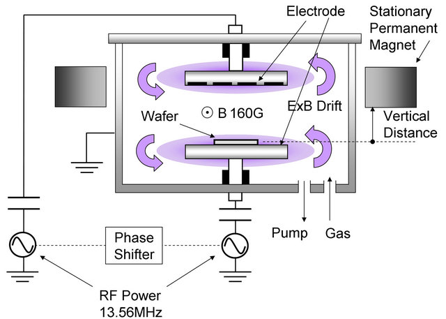
Figure 1. Schematic of the uniform supermagnetron plasma CVD apparatus with a stationary permanent magnet.
to form uniform supermagnetron plasma over the cathode, as shown in the figure. The dimensions of each flat cathode surface were about 110 × 110 mm square. Two different rf power sources with the same rf frequency (13.56 MHz) were supplied to the two electrodes inserted into a grounded metal chamber. The front surface of the upper electrode was covered with a graphite plate. The phase difference between the two rf voltages was controlled to be approximately 180˚ using a phase shifter. The lower electrode (substrate holder) was heated to 90˚C and 30˚C for the silicon dioxide (SiO2) and a-CNx:H depositions, respectively. As deposition gases, tetraethylorthosilicate (TEOS; 5 sccm)/O2 (80 sccm) and isobutane (i-C4H10; 15 sccm)/N2 (35 sccm) were used for silicon dioxide (SiO2) and a-CNx:H depositions, with gas pressures controlled at 9.3 Pa and 4 Pa, respectively. The film thicknesses were measured by profilometry (ULVAC DECTAK-3). The bonding configuration of the SiO2 film deposited in this experiment was measured using a Fourier transform infrared (FTIR) spectrometer (JIR WINSPEC-50). The thickness of the SiO2 film used in FTIR analysis was controlled to be about 830 nm. The film hardness was evaluated using a dynamic ultra-micro-hardness tester (Shimadzu DUHW201). The nitrogen and oxygen atom concentrations were measured by X-ray fluorescence spectroscopy (XRFS; Rigaku ZSX Prims).
3. Results and Discussion
First, SiO2 films were formed on Si wafers to evaluate the uniformity of deposited films using the uniform supermagnetron plasma CVD apparatus under a stationary magnetic field. The source gases of TEOS and O2 (5/80 sccm) were introduced into the CVD chamber through two mass flow controllers, and the gas pressure and wafer temperature were maintained at 9.3 Pa and 90˚C, respectively. The FTIR absorption spectrum was measured for SiO2 film deposited at upper electrode rf power (UPR F) of 100 W and a lower electrode rf power (LORF) of 300 W, as shown in Figure 2. Two sharp peaks of absorption were clearly observed at 820 cm−1 (Si-O-Si bending vibration) and 1090 cm−1 (Si-O-Si stretching vibration) [12].
SiO2 film thickness uniformities on the 4-inch Si wafers were measured as a function of the location of the stationary permanent magnet. The magnet distance was measured as the vertical distance from the top surface of the wafer placed on the lower electrode to the bottom surface of the permanent magnet, as shown in Figure 1. Figure 3 shows the SiO2 film thickness distribution observed on 4-inch Si wafers. The mean film thickness of these deposited SiO2 films was about 1 µm. Film uniformity was defined as ± [(maximum film thickness – minimum thickness)/(maximum thickness + minimum thickness)] × 100%. The film thickness distribution was symmetric at the center, where it peaked. The uniformity area, where the film thickness remained within ±5% difference, is shown to gradually increase as the magnet distance increased. Thickness uniformity was evaluated as a function of radial distance from the center, as shown in Figure 4. In the case of magnet distance of ±0 and −2 cm,
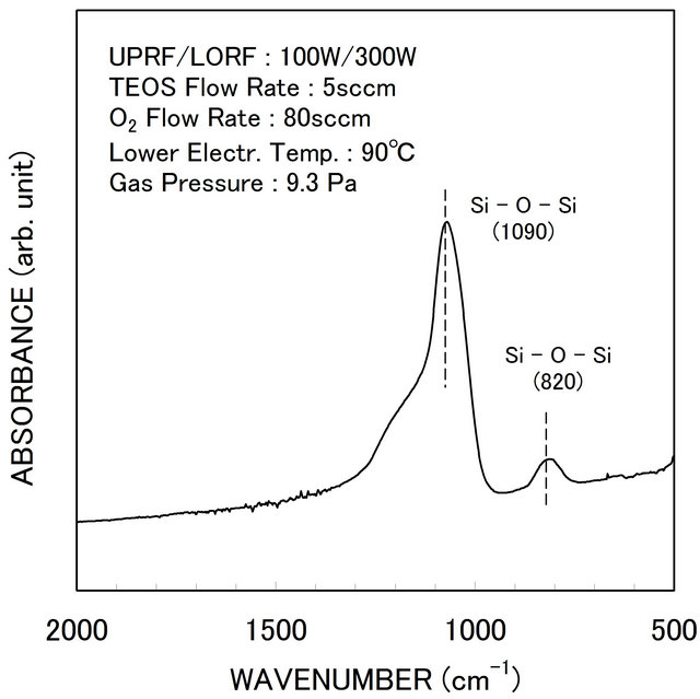
Figure 2. FTIR absorption spectra of SiO2 film deposited using the uniform supermagnetron plasma CVD apparatus.
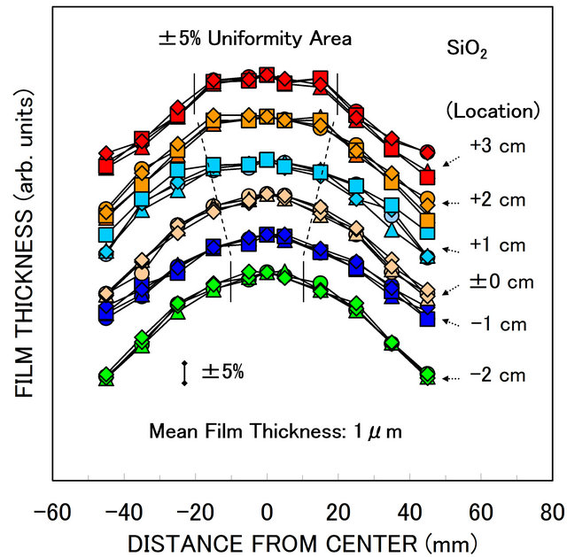
Figure 3. SiO2 film thickness distribution observed on 4- inch Si wafers as a function of permanent magnet location.
the increase rate with radial distance from the center was relatively high. In the case of the magnet distance of +3 cm from the center, it was relatively low. In the case of +3 cm magnet distance, a high uniformity of ±5% could be obtained in the 2-inch wafer region.
This uniform supermagnetron plasma CVD apparatus under a stationary magnetic field was applied to a-CNx:H film deposition. In this experiment, the source gases of i-C4H10 and N2 (15/35 sccm) were introduced into a CVD chamber through two mass flow controllers, and the gas pressure and wafer temperature were maintained at 4 Pa and 30˚C, respectively.
The deposition rate of a-CNx:H films was measured as a function of UPRF at the set LORF of 500 W, as shown in Figure 5. The deposition rate changed little with changes in UPRF and was about 100 ± 15 nm/min. From this experiment, it seems that the deposition rate depended mainly on LORF. In this case, the dc self-bias voltage (Vdc) of the lower electrode was about −170 V independent of UPRF. Therefore, the deposition rate is thought to be strongly dependent on the Vdc of the lower
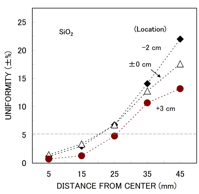
Figure 4. SiO2 film thickness uniformity evaluated as a function of distance from the center.
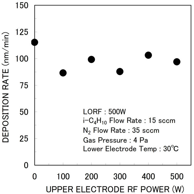
Figure 5. Deposition rate of a-CNx:H films measured as a function of UPRF at a LORF of 500 W.
electrode. Bombarding positive ions on the substrate placed on the lower electrode caused the synthesis of films. As the magnitude of Vdc of the upper electrode was relatively low (≤170 V), sputtered materials from the upper electrode were slight and the contribution of UPRF might be negligible. A high deposition rate of about 100 ± 15 nm/min was obtained in spite of a very low Vdc of −170 V. This high deposition rate was caused by the generation of high-density plasma using this uniform supermagnetron plasma CVD apparatus.
The hardness of the generated a-CNx:H films was measured as a function of UPRF at LORF of 500 W, as shown in Figure 6. Hardness changed little with UPRF and was about 24 ± 3 Pa. These values were slightly higher than that of vitreous silica (SiO2), which we measured as 22 GPa. Such a high hardness was ascribed to the inclusion of the three-dimensional configuration of sp3 C-C bonds. In spite of a Vdc as low as −170 V, high hardness was achieved using this uniform supermagnetron plasma CVD apparatus. We concluded that this supermagnetron plasma CVD apparatus is suited for synthesizing hard a-CNx:H films under operation at a very low Vdc of −170 V.
The nitrogen and oxygen atom concentrations of the formed a-CNx:H films were measured as a function of the UPRF at a set LORF of 500 W using XRFS, and are shown in Figure 7. The minimum nitrogen concentration of 11.0 mass% was obtained at an UPRF of 0 W. With the increase of UPRF from 0 W to 300 W, the nitrogen concentration was increased up to 16.5 mass%. With further increase of UPRF from 300 W to 500 W, the nitrogen concentration decreased to 15.0%. The oxygen concentration was negligible, below 1%. Despite the only slight changes of deposition rate (Figure 5) and hardness (Figure 6) with an increase in UPRF, the nitrogen concentration showed very large changes, indicating a strong dependence on UPRF. With the increase of UPRF from 0 W to 300 W, the density of positive nitrogen ions gener-
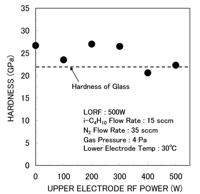
Figure 6. Hardness of a-CNx:H films measured as a function of UPRF at a LORF of 500 W.
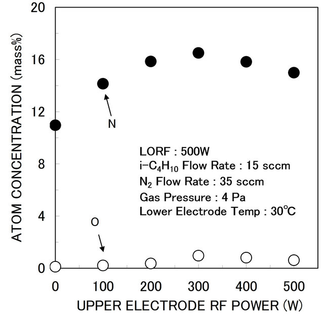
Figure 7. Nitrogen and oxygen atom concentrations of the formed a-CNx:H films measured as a function of UPRF at a set LORF of 500 W using XRFS.
ated over the upper electrode was increased and the number of CN molecules sputtered from the upper electrode to the lower electrode increased. With a further increase of UPRF from 300 W to 500 W, the Vdc of upper electrode was increased and the energy of positive N ions was also increased. As the N ion energy increased, many impinging N ions became embedded in the surface of the graphite plate placed on the upper electrode. As these embedded N ions increased in number, the number of CN molecules sputtered toward the lower electrode likely decreased. The high nitrogen concentration (11.0 - 16.5 mass%) achieved in this experiment was due to the high plasma density achieved by the uniform supermagnetron plasma CVD apparatus.
4. Conclusion
A uniform supermagnetron plasma CVD apparatus under a stationary magnetic field was applied to SiO2 and a-CNx:H film formation. Film thickness uniformity was evaluated using SiO2 CVD films, and the best uniformity was obtained at a permanent magnet location of +3 cm over the lower electrode. a-CNx:H films were deposited at the high deposition rate of about 100 ± 15 nm/min and at a very low substrate Vdc of −170 V. In this deposition condition, hard a-CNx:H films (24 ± 3 Pa) were successfully deposited. Despite the low substrate Vdc of −170 V, high nitrogen concentrations of 11.0 - 16.5 mass% were achieved. This high nitrogen concentration of a-CNx:H films was caused by the high plasma density and low substrate Vdc of this uniform supermagnetron plasma CVD apparatus under a stationary magnetic field.
REFERENCES
- M. Zhang, Y. Nakayama and M. Kume, Solid State Communications, Vol. 110, 1999, pp. 679-683. doi:10.1016/S0038-1098(99)00142-8
- R. Reyes, C. Legnani, P. M. Ribeiro Pinto, M. Cremona, P. J. G. de Araújo and C. A. Achete, Applied Physics Letters, Vol. 82, 2003, pp. 4017-4019. doi:10.1063/1.1581000
- K. Sakurai, H. Kinoshita, G. Ohno, Y. Nakanishi and M. Kubota, Japanese Journal of Applied Physics, Vol. 47, 2008, pp. 7216-7219. doi:10.1143/JJAP.47.7216
- H. Kinoshita and H. Suzuki, Journal of Modern Physics, Vol. 2, 2011, pp. 398-403. doi:10.4236/jmp.2011.25049
- J. Robertson, Journal of Vacuum Science and Technology B, Vol. 17, 1999, pp. 659-665. doi:10.1116/1.590613
- Y. Umehara, S. Murai, Y. Koide and M. Murakami, Diamond and Related Materials, Vol. 11, 2002, pp. 1429- 1435. doi:10.1016/S0925-9635(02)00042-0
- H. Kinoshita, M. Yamashita and T. Yamaguchi, Japanese Journal of Applied Physics, Vol. 45, 2006, pp. 8401- 8405. doi:10.1143/JJAP.45.8401
- H. Kinoshita, T. Ishida and S. Ohno, Journal of Applied Physics, Vol. 62, 1987, pp. 4269-4272. doi:10.1063/1.339100
- K. E. Davies, M. Gross and C. M. Horwitz, Journal of Vacuum Science and Technology A, Vol. 11, 1993, pp. 2752-2757. doi:10.1116/1.578637
- S. Bui, J. Sasserath and E. Ghanbari, Journal of Vacuum Science and Technology A, Vol. 10, 1992, pp. 1238-1243. doi:10.1116/1.578233
- H. Kinoshita, S. Nomura and M. Honda, Journal of Vacuum Science and Technology A, Vol. 18, 2000, pp. 367- 371. doi:10.1116/1.582194
- K. Sano, S. Hayashi, S. Wickramanayaka and Y. Hatanaka, Thin Solid Films, Vol. 281-282, 1996, pp. 397-400. doi:10.1016/0040-6090(96)08701-9