Journal of Modern Physics
Vol. 2 No. 11 (2011) , Article ID: 8630 , 8 pages DOI:10.4236/jmp.2011.211157
Spontaneous Spin Polarization of Electrons by Diluted Magnetic Heterostructures
1Department of Chemical Engineering and Green Energy Center, College of Engineering, Kyung Hee University, Gyeonggi, South Korea
2Government Arts College, Madurai, India
E-mail: *a.john.peter@gmail.com
Received January 13, 2011; revised February 25, 2011; accepted March 26, 2011
Keywords: Spin Polarized Transport, Spin Injection, Spin-Orbit Coupling, Resonant Tunneling
ABSTRACT
The spin dependent electron transmission phenomenon in a diluted resonant semiconductor heterostructure is employed theoretically to investigate the output transmission current polarization at zero magnetic field. Transparency of electron transmission is calculated as a function of electron energy and the well width, within the one electron band approximation along with the spin orbit interaction. Enhanced spin-polarized resonant tunneling in the heterostructure due to Dresselhaus and Rashba spin-orbit coupling induced splitting of the resonant level is observed. We predict that a spin-polarized current spontaneously emerges in this heterostructure and we estimate theoretically that the polarization can reach 40%. This effect could be employed in the fabrication of spin filters, spin injectors and detectors based on non-magnetic semiconductors.
1. Introduction
Spin-polarized injection of electrons into semiconductor has attracted a rapidly growing interest due to its potential application in spintronics devices recently. During the last years the fabrication and characterization of diluted magnetic semiconductors (DMSs) nanostructures has rapidly evolved. The essential effort of the scientists is concentrated on studying of the spin-polarized transport in nanosize multilayer structures, which are including alternating layers of ferromagnetic metals and nonmagnetic semiconductors. Operation of a spintronic device requires efficient spin injection into a semiconductor, spin manipulation, control and transport, and spin detection.
Owing to the possibility of controlling and probing magnetic properties by the electronic subsystem or vice versa, DMSs have successfully been employed to address a number of important questions concerning the nature of various spin effects in various environments and at various length and time scales. At the same time, DMS exhibit a strong sensitivity to the magnetic field and temperature as well as constitute important media for generation of spin currents and for manipulation of localized or itinerant spins by, e.g., strain, light, electrostatic or ferromagnetic gates. These properties, complementary to both non-magnetic semiconductors and magnetic metals, open doors for application of DMSs as functional materials in spintronic devices. The spin injection was realized successfully utilizing the tunneling through diluted magnetic semiconductor junction [1], but it still needs some undesirable effort to overcome strong external magnetic field and the low Curie temperature of DMSs. Hopefully, it was recently discovered that the joint action of the Rashba spin-orbit interaction (SOI) and in-plane magnetic field on electrons confined in onedimensional quantum wires (QW) results in unique properties [2-4]. Several useful applications based on these properties were proposed, including a scheme for measuring nuclear spin polarization [2], a spin filter [3], spintronic devices [5,6] and quantum computing [7,8]. Recent experimental advances have allowed generation and control of non-equilibrium spin polarization in semiconductor structures [9-11]. One of the main obstacles for these potential applications is to inject highly spin-polarized carriers into semiconductors. The spin polarized current through a diluted magnetic semiconductor junction was predicted theoretically [12], demonstrated experimentally by applying a strong magnetic field at low temperatures [1] and the s-d model containing a description of band electrons coupled to localized spins is used to calculate the intrasubband spin-flip lifetime due to scattering of electrons by magnons in Cd1-xMnxTe quantum well structures [13].
Advances in modern epitaxial growth technologies such as Molecular-Beam Epitaxy and Metalorganic Chemical Vapor Deposition have paved the way with an opportunity to produce semiconductor heterostructures in which the material parameters can be changed over a wide range and controlled within considerable accuracy. This level of quality allows the relevant theoretical analysis within the framework of relatively simple approximations for semiconductor band structures. So it is worthwhile to investigate how to obtain spin-polarized electronic current using the spin-splitting effect in the resonant transmission heterostructures. Spin-orbit interaction couples spin states and space motion of conduction electrons in the plane perpendicular to growth direction that opens a possibility to polarize, manipulate and detect spins by moderate electrical field. The effect of Rashba spin-orbit interactions due to in-built or external electric field on the spin polarized transport in the case of a non-magnetic semiconductor heterostructure has been theoretically investigated and it is reported that the spin polarization can reach 40% to 50% with moderate electric fields [14,15]. Recently, it is predicted that the zerofield spin-dependent electron tunneling with spin polarization of 20% even in the case of a nonmagnetic semiconductor if the system lacks center of inversion [16]. John Peter [17] has shown the polarization efficiency raises upto 45% when non-magnetic asymmetric quantum well is used. Qing-feng Sun et al., [18] proposed a novel scheme to efficiently polarize and manipulate the electron spin in a quantum dot showed that the direction and the strength of the spin polarization is well controllable and manipulatable by simply varying the bias or the gate voltage. However, in the case of symmetric potential barriers, the interface spin-orbit coupling does not lead to a dependence of tunneling on the spin orientation. Spin-dependent resonant tunneling in non-magnetic semiconductor heterostructures has prominent perspectives in the emerging field of spintronics. Devices based on spin-dependent tunneling are suggested for utilization as components in the spin-field-effect transistor. Spontaneous spin-polarized current in a nonuniform Rashba interaction system has been studied recently [19] wherein they have demonstrated a spontaneous spin-polarized current emerges in the absence of any magnetic material and magnetic field due to the combination of the coherence effect and the Rashba interaction.
In this letter, we analyze the spin-dependent transmission phenomenon in resonant transmission structures. The spin-polarized electronic current is due to spin splitting of electronic bands in asymmetric heterostructures. We investigate the spin-polarized transport through a heterostructure which does not include any magnetic material and magnetic field, only has the spin-orbit coupling. We predict that a spin-polarized current spontaneously emerges in this heterostructure. The spin-polarized transmission current in resonant transmitting heterostructures at zero magnetic field is studied. We demonstrate that asymmetry of the electron distribution in the electrode regions with spin depended transmission probability can provide output current polarization. Transparency of electron transmission through a diluted magnetic heterostructure of CdTe/CdMnTe/CdTe has been calculated as a function of electron energy as well as the well width using the proposed model which includes the combined effects of Dresselhaus and in-plane Rashba spin-orbit interactions, within the one electron band approximation. The proposed model for the calculation of transmission coefficients and the polarization efficiency in the well system with Rashba and Dresselhaus spinorbit coupling is described in Section 2. The results of the numerical calculations obtained by transfer matrix approach are presented in Section 3.
2. Spin-Dependent Transmission Probability
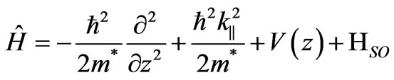
We consider the transmission of electrons with the initial wave vector  through a diluted magnetic heterostructure, CdTe/CdMnTe/CdTe grown along z|| [001] as shown in Figure 1. Here k|| is the wave vector in the plane of the interfaces, and kz is the wave vector component normal to the barrier and pointing in the direction of transmission. The electron motion in each layer of the structure is described by the Hamiltonian [20],
 (1)
(1)
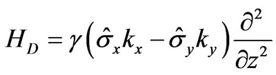
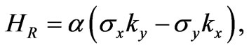
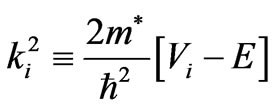
where m* is the electron effective mass, V(z) is the heterostructure potential as shown in Figure 1, and HSO is the spin-dependent contribution to the effective Hamiltonian equal to the sum of HD and HR as given below. HD is the spin-dependent k3 Dresselhaus term and HR is the in-plane Rashba term, both describing the spin splitting of conduction electrons in zinc-blende-lattice semiconductors. Assuming that the barrier structure has been designed such that the kinetic energy ε is much smaller than the barrier height V0, the Dresselhaus term [21,22] is simplified to,
 (2)
(2)
and in the asymmetrical quantum wells in-plane Rashba term exists with non-zero α due to heteropotential asymmetry [23]
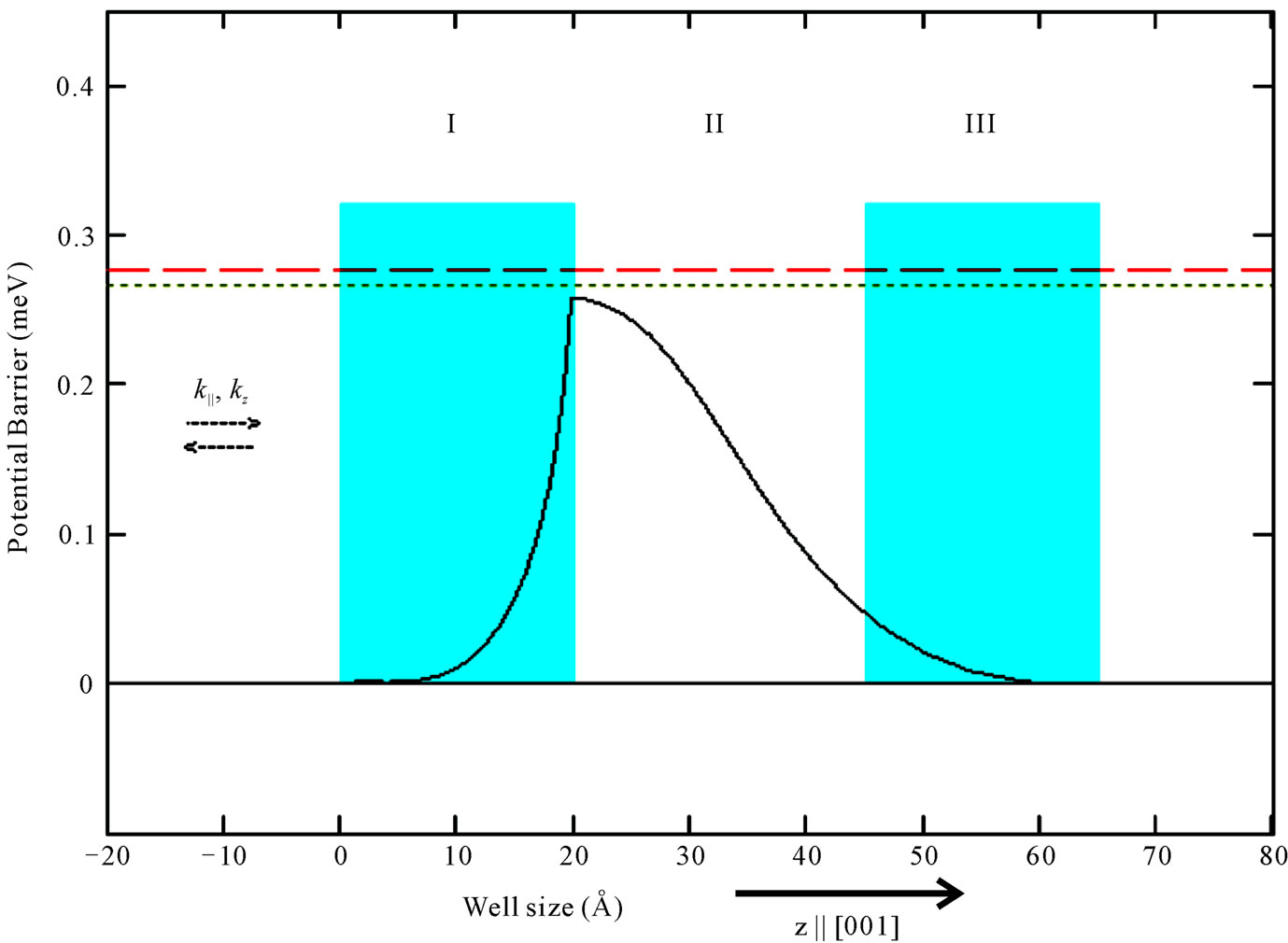
Figure 1. Flat band symmetric CdTe/CdMnTe/CdTe well heterostructure. The barrier height is taken as 320 meV and the well size is 25 Å. Espin up is 0.1691 eV and Espin down is 0.14182 eV for the first state. Transmission of electrons with the wave vector k = (k||, kz) through the potential barrier V of width a grown along z.
 (3)
(3)
where  is a material constant,
  and
and  are the Pauli matrices, and the coordinate axes x, y, z are assumed to be parallel to the cubic crystallographic axes [100], [010], [001], respectively.
For the fixed in-plane wave vector k||, the wave functions of the electrons are of the form
 (4)
(4)
where ρ = (x, y) is an in-plane coordinate of the barrier and  is a spinors. The electrons propagating through well are described in the regions I, II and III (see Figure 1) as below [24]
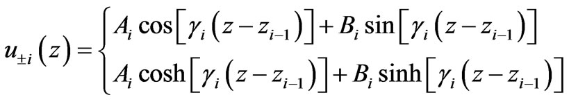 for
for 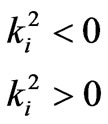 (5)
(5)
where
 and
and 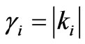
where
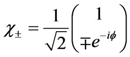
The Dresselhaus term (2) is diagonalized by the spinors [21]
 (6)
(6)
which describe the electron states “+” and “–” of the opposite spin directions. Here  is the polar angle of the wave vector k in the plane of the barrier and
 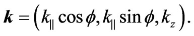 The eigen spin states “+” and “–” propagate through the well with conservation of the spin orientation.
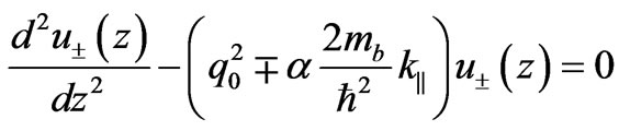
With the diagonalized Dresselhaus spin-orbit coupling term, the electron behavior in the well is described by
 . (7)
. (7)
Therefore, the wave vector  through the well is given by [21]
 (8)
(8)
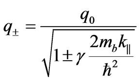
where  is the reciprocal length of decay of the wave function in the well when the spin-orbit interactions are omitted as given by
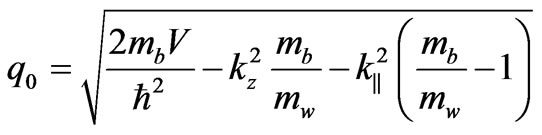 (9)
(9)
Here mb and mw are the electron effective masses in the barrier and well respectively.
In the proposed model the effect of the in-plane Rashba spin-orbit interaction on the spin dependent tunneling through double barrier is described by diagonalizing the in-plane Rashba term (Equation (3)) by the same spinors (Equation (6)),which are used to diagonalize the Dresselhaus term, and we derive,
 . (10)
The Equation (10) describes the electron behavior in the barrier with the in-plane Rashba spin-orbit coupling with the wave vector  through the well
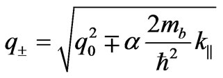 . (11)
Hence the combined effect of Dresselhaus and Rashba spin interactions on the spin dependent transmitting through the well is described by
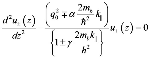 , (12)
The wave vector  through the well including both Dresselhaus and in-plane Rashba spin-orbit coupling can therefore be
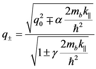 (13)
(13)
The transmission coefficient  is calculated by transfer matrix approach [25] and the spin polarization efficiency P that determines the difference of transparency for the spin states “+” and “–” through the barrier is
 . (14)
3. Numerical Results and Conclusions
We have chosen CdTe and CdMnTe because of the same crystal structures and lattice constants. The relevant parameters for CdTe are Eg = 1.606 eV, m = 0.67 me and for CdMnTe, Eg = 1.587 eV, m = 0.67 me, k|| = 2 × 10⁸ m–1 and α = 8.73 × 10⁻¹² eV. The suitable parameter for the barrier height of CdTe is 0.32 eV. In the numerical calculations, we choose the system size to be: well width, b = 25 Å, barrier thickness, a = 20 Å, and the barrier height, V = 320 meV. The real part of the transmitting total wave function corresponding to E = 0.28672 eV is shown in Figure 1. Espin up is 0.265245 eV and Espin down is 0.276529 eV for the first state. Transmission of electrons with the wave vector through the potential barrier V of width is grown along z. The transmission resonances occur nearly at the discrete energy values corresponding to the well. The transparency  and the spin polarization efficiency P of symmetrical well of heterostructure of CdTe/CdMnTe/CdTe with fixed k|| = 2 × 10⁸ m–1 have been calculated as a function of electron energy as well as the well width and the results are presented in Figures 2 to 5. wherein the first transmission resonance occurs at the discrete energy value, 0.28672 eV, for a given value of V. These figures show the polarization efficiency P, as a function of the electron energy with Dresselhaus spin-orbit term and the Rashba term and combined effects of both the effects.
Figure 2 shows the transparency Tup, Tdown, and the polarization efficiency P, of the CdTe/CdMnTe/CdTe symmetrical well hetero structure as a function of the electron energy at fixed k|| = 2 × 10⁸ m–1 with Dresselhaus spin-orbit term. It is seen that both the spin-up and spin down electrons are transmitted completely showing resonant transmission. However, this transmission resonance occurs at different incident energy for different values of k. At a given initial wave vector of electrons, the polarization efficiency shows the peak value for every bound states with the strength of the Dresselhaus spin-orbit coupling (Equation (8)). However, this peak is broadened, resonance peaks shift to lower-energy regions and their corresponding transmission spectrum becomes more complex for higher bound states.
Figure 3 displays the transparency Tup, Tdown, and the polarization efficiency P, of the CdTe/CdMnTe/ CdTe symmetrical well hetero structure as a function of the electron energy at fixed k|| = 2 × 10⁸ m–1 with Rashba spin-orbit term. It is seen that both the spin-up and spin down electrons are transmitted completely showing resonant transmission. The first transmission electron energy occurs earlier for spin up electrons. The polarization efficiency decreases drastically with the strength of the Rashba spin-orbit coupling upto the first discrete energy value and then increases beyond this value of electron energy (Equation (11)). However, this peak is broadened for higher bound states and resonance peaks shift to lower-energy regions.
Similar calculations have been reported earlier in the literature but for the case of non-magnetic semiconductors. The effect of Rashba spin-orbit interactions due to
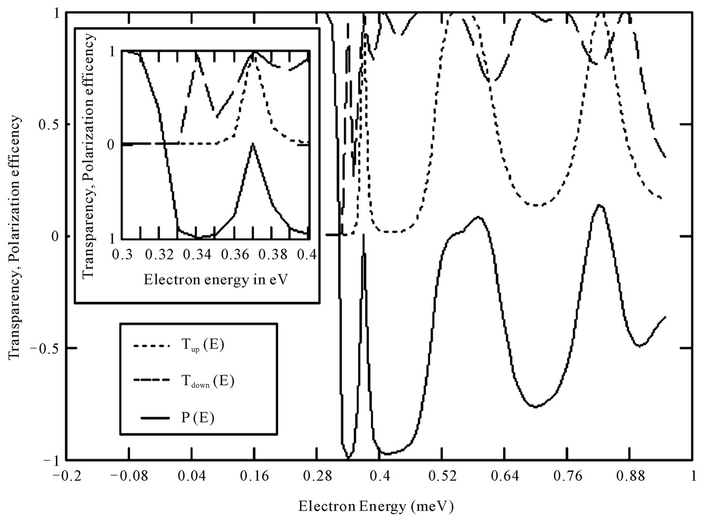
Figure 2. The transparency Tup, Tdown, and the polarization efficiency P, of the CdTe/CdMnTe/CdTe a symmetrical barrier hetero structure as a function of the electron energy at fixed k|| = 2 × 10⁸ m–1 with Dresselhaus spin-orbit term. Well width, b = 25 Å, barrier thickness, a = 20 Å and the barrier height, V = 320 meV. The inset figure shows the transparency and the polarization efficiency for the range of energy between 0.30 eV and 0.40 eV.

Figure 3. The transparency Tup, Tdown, and the polarization efficiency P, of the CdTe /CdMnTe/CdTe symmetrical barrier hetero structure as a function of the electron energy at fixed k|| = 2 × 10⁸ m–1 with Rashba spin-orbit term. Well width, b = 25 Å, barrier thickness, a = 20 Å and the barrier height, V = 320 meV.
in-built or external electric field on the spin polarized transport has been theoretically computed and reported that the spin polarization can reach 40% to 50% with moderate electric fields [246]. Moreover, it is predicted that the zero-field spin-dependent electron tunneling with spin polarization of 20% even in the case of a nonmagnetic semiconductor if the system lacks center of inversion [21].
Figure 4 shows the transparency Tup, Tdown, and the polarization efficiency P, of the CdTe/CdMnTe/CdTe symmetrical well hetero structure as a function of the electron energy at fixed k|| = 2 × 10⁸ m–1 including both Dresselhaus and Rashba spin-orbit coupling terms. It is seen that both the spin-up and spin down electrons are transmitted completely showing resonant transmission. As spin-up electrons see shallower well compared to spin-down electrons, the spin down electron shows the lower transmission coefficients than the transmission coefficients of spin-up electrons. Also the spin-up and spin-down resonances are separated on energy scale by less than 1 meV. However there occurs a drastic increase in polarization efficiency with both the spin orbit coupling terms are included (Equation (13)). Eventually this figure shows the enhancement of the efficiency of polarization when both the spin orbit terms are included. Carlos Egues [27] has reported similar results in the case of a diluted magnetic semiconductor.
In Figure 5, the polarization efficiency as a function of a well width qoa is plotted. The solid and dotted curves correspond respectively to the variation of the reflected and transmission coefficients for a rectangular potential barrier. The polarization strongly depends on the electron wave vector k|| parallel to the barrier. This result suggests a device for spin injection into quantum wells assuming two quantum wells separated by a tunneling barrier and a current flowing along one of the quantum wells. The in-plane current results in nonzero average electron wave vector k|| in a spin polarization of carriers. The k3 Dresselhaus terms in the effective Hamiltonian of bulk semiconductor of the barrier are shown to be depended of the tunnelling and transmission on the spin orientation [21]. The polarization efficiency is found to be about 60% in our calculation when compared to non-magneitc materials having the efficiency less the 40% [17].
4. Conclusions
In conclusion, the result suggests the fabrication of spin filters and a device for spin injection into quantum wells, on the base of the diluted magnetic heterostructures. Spin-dependent resonant tunneling in diluted magnetic
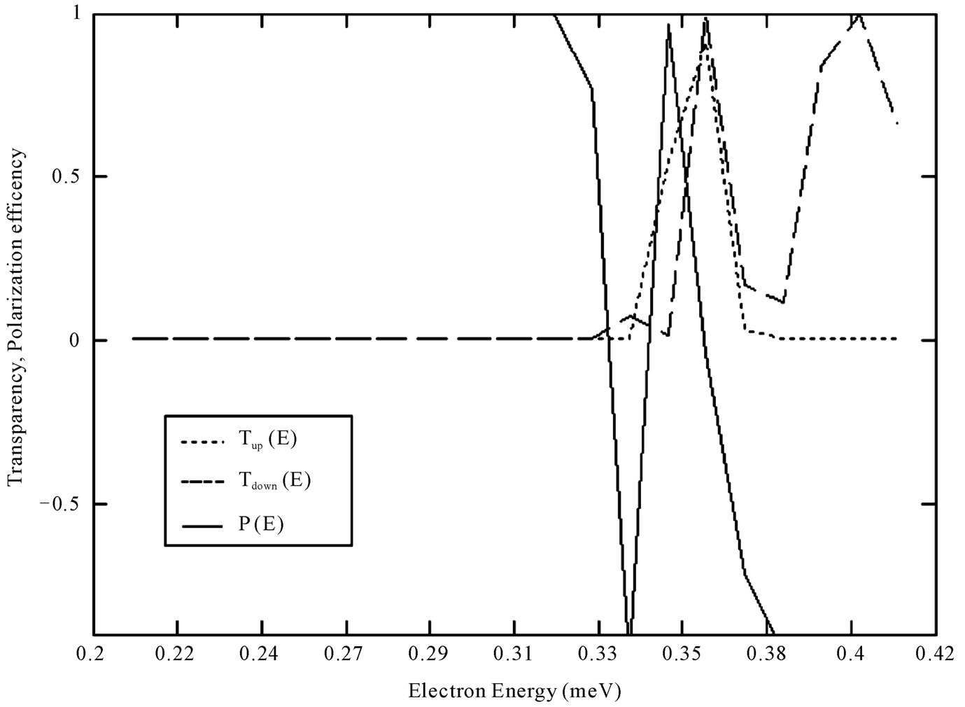
Figure 4. The transparency Tup, Tdown, and the polarization efficiency P, of the CdTe/CdMnTe/CdTe symmetrical barrier hetero structure as a function of the electron energy at fixed k|| = 2 × 10⁸ m–1 including both Dresselhaus and Rashba spin-orbit terms. Well width, b = 25Å, barrier thickness, a = 20 Å,  and the barrier height, V = 320 meV.
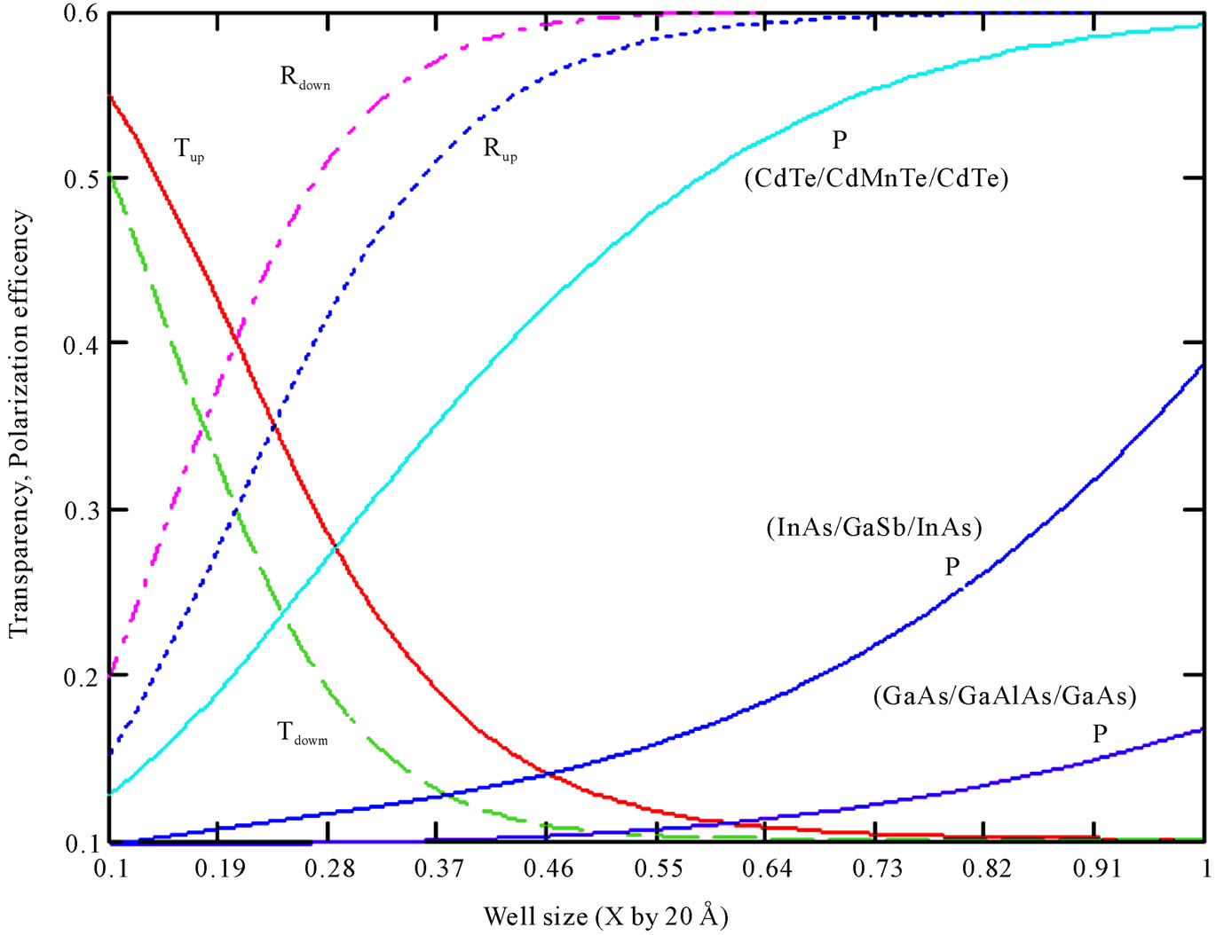
Figure 5. The transparency Tup, Tdown, Rup, Rdown and the polarization efficiency P, of the CdTe/CdMnTe/CdTe, InAs/GaSb/ InAs (Ref. [17]) and GaAs/GaAlAs/GaAs (Ref. [17]) heterostructures as a function of the well width at fixed k|| = 2 × 10⁸ m–1 including both Dresselhaus and Rashba spin-orbit terms. Well width, b = 25 Å, barrier thickness, a = 20 Å and the barrier height, V = 320 meV.
semiconductor heterostructures has prominent perspectives in the emerging field of spintronics. We would like to point out that the calculations presented use a simple model of the resonant transmission structures through a heterostructure and a simple one electron band approximation with spin-orbit coupling. The heterostructure does not include any magnetic material and magnetic field, only has the spin-orbit coupling. And we predict that a spin-polarized current spontaneously emerges in this heterostructure. Due to the combination of the coherence effect and the Rashba interaction, a spontaneous spin-polarized current emerging in the absence of any magnetic material and magnetic field has been studied recently [19]. Thus the spin-polarized current is generated without a magnetic field is good agreement with their results. However, the structures have realistic parameters but the proposed estimate of the total polarized current is only a starting point of the investigation of this new effect. The effect of Dresselhaus and Rashba spinorbit interactions could be favorably engineered for fabricating spin injectors and detectors based on non-magnetic semiconductors [28]. We have demonstrated that the k3 Dresslhaus terms in the effective Hamiltonian of semiconductors lacking a center of inversion yield a considerable spin polarization of electrons transmitting through the well. This effect could be employed for creating spin filters. Further experimental investigations of the effects in the areas like spintronics and nanocomputers, we hope that the present work will stimulate more experimental activities to lend support to our calculations.
5. Acknowledgements
The author thanks the CSIR, India for the grant (No.03 (1159)/10/EMR-II) for the financial support of this work.
REFERENCES
- Y. Ohno, D. K. Young, B. Beschoten, F. Matsukura, H. Ohno and D. D. Awschalom, “Electrical Spin Injection in a Ferromagnetic Semiconductor Heterostructure,” Nature, Vol. 402, 1999, pp. 790-792. doi:10.1038/45509
- J. A. Nesteroff, Y. V. Pershin and V. Privman, “Polarization of Nuclear Spins from the Conductance of Quantum wire,” Physical Review B, Vol. 69, 2004, Article ID 121306(R).
- P. Středa and P Šeba, “Antisymmetric Spin Filtering in One-Dimensional Electron Systems with Uniform Spin-Orbit Coupling,” Physical Review Letters, Vol. 90, No. 25, 2003, Article ID 256601. doi:10.1103/PhysRevLett.90.256601
- Y. V. Pershin and C.Piermarocchi, “Relaxation of Conduction Electron Spins in Semiconductors,” Applied Physics Letters, Vol. 86, No. 21, 2005, Article ID 212107, pp. 1-3. doi:10.1063/1.1935747
- G. A. Prinz, “Spin-Polarized Transport,” Physics Today, Vol. 48, No. 4, 1995, p. 58.
- G. A. Prinz, “Magnetoelectronics,” Science, Vol. 282, 1998, pp. 1660-1663. doi:10.1126/science.282.5394.1660
- D. Loss and D. P. DiVincenzo, “Quantum Computation with Quantum Dots,” Physical Review A, Vol. 57, No. 20, 1998, pp. 120-123.
- B. E. Kane, “A Silicon-Based Nuclear Spin Quantum Computer,” Nature, Vol. 393, 1998, pp. 133-137. doi:10.1038/30156
- S. Das Sarma, “Spintronics,” American Science, Vol. 89, 2001, p. 516.
- D. D. Awschalom, M. E. Flatte and N. Samarth, “Spintronics,” Scientific American, Vol. 286, 2002, pp. 66-73. doi:10.1038/scientificamerican0602-66
- H. Akinaga and H. Ohno, “Semiconductor Spintronics,” IEEE Transactions on Nanotechnology, Vol. 1, No. 1, 2002, pp. 19-31. doi:10.1109/TNANO.2002.1005423
- J. C. Egues, “Spin-Dependent Perpendicular Magnetotransport through a Tunable ZnSe/Zn1–xMnxSe Heterostructure,” Physical Review Letters, Vol. 80, No. 20, 1998, pp. 4578-4581. doi:10.1103/PhysRevLett.80.4578
- E. Souto, O. A. C. Nunes, F. M. S. Lima, D. A. Agrello and A. L. A. Fonseca, “Spin Waves Amplification in Antiferromagnetic Semiconductors Stimulated by Infrared Laser Field,” Physical Review B, Vol. 68, No. 12, 2003, Article ID 125317. doi:10.1103/PhysRevB.68.125317
- A. Voskoboynikov, S. S. Liu, C. P. Lee and O. Tretyak, “Spin-Dependent Tunneling in Double-Barrier Semiconductor Heterostructures,” Physical Review B, Vol. 59, No. 19, 1999, pp. 12514-12520.
- A. de Andrada e Silva and G. C. La Rocca, “ElectronSpin Polarization by Resonant Tunneling,” Physical Review B, Vol. 59, No. 24, 1999, pp. 15583-15585. doi:10.1103/PhysRevB.59.R15583
- V. I. Perel’, S. A. Tarasenko, I. N. Yassievich, S. D. Ganichev, V. V. Bel’kov and W. Prettl, “Spin-Dependent Tunnelling through a Symmetric Barrier,” Physical Review B, Vol. 67, No. 20, 2003, Article ID 201304. doi:10.1103/PhysRevB.67.201304
- A. J. Peter, “Electron-Spin Polarization on a Non-Magnetic Heterostructure,” Phyics Letters A, Vol. 372, No. 31, 2008, pp. 5239-5242. doi:10.1016/j.physleta.2008.06.025
- Q.-F. Sun and X. C. Xie, “Bias-Controllable Intrinsic Spin Polarization in a Quantum Dot,” Physical Review B, Vol. 73, No. 23, 2006, Article ID 235301. doi:10.1103/PhysRevB.73.235301
- Q.-F. Sun and X. C. Xie, “Spontaneous Spin-Polarized Current in a Nonuniform Rashba Interaction System,” Physical Review B, Vol. 71, No. 15, 2005, Article ID 155321. doi:10.1103/PhysRevB.71.155321
- M. M. Glazov, P. S. Alekseev, M. S. Odnoblyudov, V. M. Chistyakov, S. A. Tarasenko and I. N. Yassievich, “Spindependent Resonant Tunneling in Symmetrical DoubleBarrier Structure,” Physical Review B, Vol. 71, No. 15, 2005, Article ID 155313. doi:10.1103/PhysRevB.71.155313
- V. I. Perel, S. A. Tarasenko, I. N. Yassievich, S. D. Ganichev, V. V. Bel’kov and W. Prettl, “Spin-Dependent Tunneling through a Symmetric Semiconductor Barrier,” Physical Review B, Vol. 67, No. 20, 2003, Article ID R201304. doi:10.1103/PhysRevB.67.201304
- G. Dresselhaus, “Spin-Orbit Coupling Effects in Zinic Blende Structures,” Physical Review, Vol. 100, No. 2, 2005, pp. 580-586. doi:10.1103/PhysRev.100.580
- Yu. A. Bychkov and E. I. Rashba, “Oscillatory Effects and the Magnetic Susceptibility of Carriers in Inversion Layers,” Journal of Physics C, Vol. 17, No. 33, 1984, p. 6093.
- A. K. Ghatak, “Basic Quantum Mechanics,” Macmillan Ind. Ltd, India, 2002, p. 242.
- E. O. Kane, “Tunneling Phenomenon in Solids,” Plenum, New York, 1969.
- A. Voskoboynikov, S. S. Liu, C. P. Lee and O. Tretyak., “Spin-Polarized Electronic Current in Resonant Tunneling Heterostructures,” Journal of Applied Physics, Vol. 87, No. 1, 2000, pp. 387-391. doi:10.1063/1.371872
- J. C. Egues, “Spin-Dependent Perpendicular Magnetotransport through a Tunable ZnSe/Zn1–xMnxSe Heterostructure: A Possible Spin Filter?” Physical Review Letters, Vol. 80, No. 20, 1998, pp. 4578-4581. doi:10.1103/PhysRevLett.80.4578
- K. C. Hall, W. H. Lau, K. Gündoğdu, E. Michael Flatteé and T. F. Boggess, “Nonmagnetic Semiconductor Spin Transistor,” Applied Physics Letters, Vol. 83, No. 14, 2003, p. 2937.