Wireless Engineering and Technology
Vol.2 No.4(2011), Article ID:8152,5 pages DOI:10.4236/wet.2011.24034
3 - 10 GHz Ultra-Wideband Low-Noise Amplifier Using Inductive-Series Peaking Technique with Cascode Common-Source Circuit
![]()
1Department of Electronic Engineering, Vanung University, Chung-Li, Taiwan, China; 2Materials & Electro-Optics Research Division, Chung-Shan Institute of Science & Technology, Taiwan, China.
Email: cswu@mail.vnu.edu.tw
Received November 4th, 2010; revised December 15th, 2010; accepted January 5th, 2011.
Keywords: Ultra-Wideband (UWB), Low Noise Amplifier (LNA), CPW, pHEMT, MMIC
ABSTRACT
The objective of this paper is to investigate a ultra-wideband (UWB) low noise amplifier (LNA) by utilizing a two-stage cascade circuit schematic associated with inductive-series peaking technique, which can improve the bandwidth in the 3 - 10 GHz microwave monolithic integrated circuit (MMIC). The proposed UWB LNA amplifier was implemented with both co-planer waveguide (CPW) layout and 0.15 μm GaAs D-mode pHEMT technology. Based on those technologies, this proposed UWB LNA with a chip size of 1.5 mm × 1.4 mm, obtained a flatness gain 3 dB bandwidth of 4 - 8 GHz, the constant gain of 4 dB, noise figure lower than 5 dB, and the return loss better than –8.5 dB. Based on our experimental results, the low noise amplifier using the inductive-series peaking technique can obtain a wider bandwidth, low power consumption and high flatness of gain in the 3 - 10 GHz. Finally, the overall LNA characterization exhibits ultra-wide bandwidth and low noise characterization, which illustrates that the proposed UWB LNA has a compact size and favorable RF characteristics. This UWB LNA circuit demonstrated the high RF characterization and could provide for the low noise micro-wave circuit applications.
1. Introduction
In the ultra-wideband (UWB) applications, the Federal Communications Commission (FCC) had offered the 7500 MHz bandwidth in the 3.1 - 10.6 GHz frequency range [1]. This new standard system provides low cost, low complexity, low power consumption, high security, and high data-rate wireless communication capabilities, which can be widely adopted in wideband high-speed telecommunication system, Wireless Local Area Networks (Wireless LANs), and Wireless Personal Area Networks (Wireless PANs). Hence, the related wideband communication systems have increasingly been investigated in recent years. The low noise amplifier (LNA) plays a critical role in the front-end receiver communication, which needs to provide a excellent RF performance, such as a good input impedance matching, a low noise figure (NF), and a flat power gain, etc [2]. In the UWB LNA circuit technology, the CMOS-based technology has been extensively to be adopted in recent years. Much attention has been devoted to the wideband LNA technology [3-5]. Yi-Jing Lin et al. [3] proposed a low noise amplifier (LNA) utilizing a current-reused technique and a simple high-pass input matching network [3]. Chih-Fan Liao et al. [4] pointed out the LNA employing a broadband noise-canceling technique [4]. Alternatively, several investigators [4,7] had studied the wideband amplifier using the inductive-series peaking method [6,7]. However, the designed circuit with the CMOS technology was still limited in the microwave monolithic integrated circuit, which might be subject to severe parasitic capacitance, lower trans-conductance, and noise performance [4,6]. Therefore, the roughly parasitic capacitance had significantly deteriorated bandwidth in the CMOS-based technology and affected the noise characterization. Typical characterization of pHEMT shows the excellent performance in the microwave frequency; hence, the GaAs pHEMT technology was employed to overcome the limitations of CMOSbased in this work.
In this paper, the UWB LNA MMIC was studied taking into account the band-pass filter as an input matching network associated with inductive peaking method [7] in the inter-stage, which could improve the noise characterization and to further extend bandwidth in the 3 - 10 GHz. In addition, considering electromagnetic (EM) coupling issue in the layout, this circuit was realized by the co-planer waveguide (CPW) technology, which greatly benefited by the unnecessary back-side fabrication, good electronic isolation property and compact drawing in the circuit layout. In other words, the CPW MMIC can not only reduce the chip size by eliminating discrete components, but also degrade the parasitic effect by wire-bonding issue. Consequently, a UWB LNA MMIC using the inductive peaking method as well as the CPW structure was adopted in this work, which was implemented by the 0.15 μm GaAs pHEMT technology.
For the objective to be achieved, this work was performed with the following procedures. Firstly, the UWB LNA MMIC was adopted a cascade architecture, which consisted of the input-stage and output-stage in the twostage circuit. The inductive peaking method was introduced in the inter-stage, which could extend the bandwidth. Next, this UWB LNA circuit was designed and simulated S-parameters by the Advanced Design System (ADS) operating at the frequency of 3 - 10 GHz. This amplifier circuit was designed to fully match the input and output impedance of 50 ohm without any external circuit. Then, the noise amplifier was fabricated by the GaAs pHEMT technology and S-parameters were measured by the Vector Network Analyzer. Measurement results were obtained a 3 dB gain bandwidth of 3 - 8 GHz, the flatness gain of 4 dB, and minimum noise figure 3 dB. Finally, the inductive peaking method associated with the CPW structure was employed in this study, which demonstrated that the proposed UWB LNA was well suitable for the microwave integrated circuits.
2. Design and Analysis the UWB LNA Structure
To fulfill the wide band-width LNA, this LNA MMIC circuit was carried out by a cascade two-stage schematic, which was adopted the input stage (M1, M2) and output stage (M3, M4) network circuit series with the inductive peaking (Lpeak) in the inter-stage, as shown in Figure 1. The input stage and output stage network circuit was worked by the cascode topology simultaneously, which was carried out by the gate length 0.15 μm GaAs pHEMT with 2 × 75 μm channel width transistor at each stage. In the meanwhile, the pHEMT device was operated at Vds of 2 V and Vgs of –1.2 V in this circuit, which the FET could work at high gain and low noise operation region. To achieve a favorable to characterization, the

Figure 1. Schematic of the proposed UWB LNA.
performances of UWB LNA circuit were simulated and verified by the Advanced Design System (ADS) momentum. Considering the matching impedance was fully designed the impedance of 50 ohm. The matching circuits were performed with the three-stage matching circuits, which contained the input port, inter-stage and output port, as also observed in Figure 1.
To obtain the optimum UWB LNA characterization, the procedures of the designed matching circuit could be expressed as follows. Firstly, the input matching network was mainly designed for wider band-width and low noise characterization. This matching network was adopted the cascode common-source topology, which could not only obtain the low power consumption, but also eliminate Miller effect [2]. Hence, the input matching network with a cascode common-source configuration should provide a better isolation from the output return signal. In addition, the degeneration inductor (LS) was directly connected to the source of input pHEMT (M1), which could perform a negative-feedback to offer the noise impedance matching and obtain the stability effect simultaneously. Next, the inductor (Lg1) could also provide the impedance matching of the pHEMT (M1), which was required to meet the wide bandwidth frequency. Then, the inductor (Lg2) could offer the impedance matching of the pHEMT (M2). Moreover, the input matching network was also executed by a two-step L-C band-pass filter configuration; namely, C0, C3, Lg3, and Lg4, which could obtain the wider band-width. On the other hand, the band-pass filter combined with a negative-feedback network to form an input matching network for achieving a wideband matching characteristic. Thus, the input stage matching network could obtain the low noise figure, available gain and impedance matching in the wide band-width simultaneously.
Secondly, this inter-stage should be designed the matching circuit, which was matched the output of the input-stage into the input of the output-stage. More specifically, the inter-stage matching network would be conjugate matched between the drain of input pHEMT (M2) and the gate of output pHEMT (M3), which was optimized to reduce the mis-matching loss in LNA circuit. Note that the inductor (Lpeak) and capacitor (C2) was employed as inter-stage, which performed a series-resonant to generate a peaking characteristic for compensation the high frequency gain roll-off in the wide bandwidth [6]. In other words, the inductor (Lpeak) was introduced to this inter-stage, which should extend the bandwidth and realize the flatness in the wide bandwidth. Finally, the inter-stage matching network could carry out both the flatness signal gain and impedance matching simultaneously.
Thirdly, the output stage was fully for achieving maximum gain. This output matching network was also adopted the cascode common-source topology. Besides, the output matching was performed by the capacitor (C7) and an inductance (Lg5) in the wide band-width. Hence, this output matching network could simultaneously execute both the available gain and impedance matching. In addition, MIM capacitors (C0, C2, and C7) were used as DC blocking, at the RF input, inter-stage, and output of the chip, respectively. Moreover, under consideration of the power consumption and the chip area, the source terminal of pHEMT device (M3) was directly connected to the ground.
Furthermore, the stability effect should be considered in the amplifier circuit. The unstable issue was resulted from the micro-strip discontinuities and electromagnetic (EM) effect in the amplifier circuit, caused by the various components coupling in the high frequency. It was beneficial that all passive components were evaluated by an EM field simulator. Therefore, the circuit stability analysis was executed for each stage in order to ensure having a sufficient margin in the wide-band circuit. Figure 2 displayed the simulation stability factors K and B for the proposed CPW wide-band LNA, which revealed the unconditional stability with K > 1 and B > 0 in the wideband region. Eventually, the stable factor of the amplifier was achieved to fulfill unconditional stable in the wide bandwidth. Consequently, the circuit parameter optimization and EM simulation based on these essential matching networks were performed, so as to achieve the required circuit performance. Eventually, the stable factor of the amplifier was achieved to fulfill unconditional stable.
Consequently, the wide band-width LNA was accomplished by a cascade two-stage matching network. In the proposed LNA topology, the cascade circuit combined
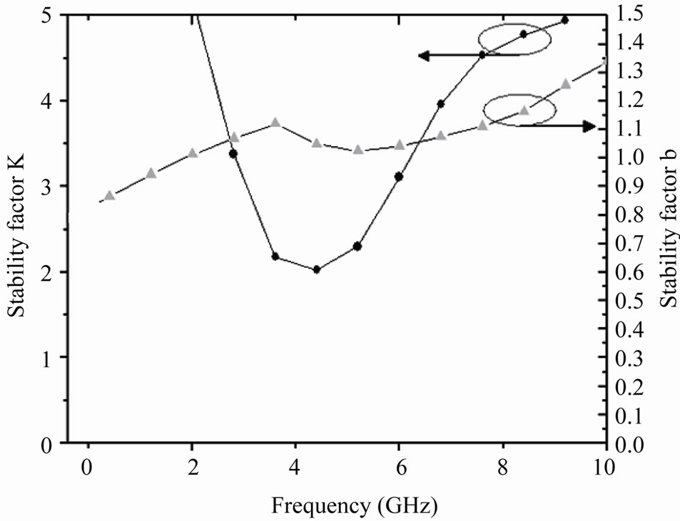
Figure 2. Calculated stability factors K and B for the proposed UWB LNA.
with degeneration inductor in the input matching network is beneficial to the low noise designed. With this inductive peaking design technique, a low noise not only can be obtained, an ultra bandwidth can also be achieved simultaneously. The circuit parameter optimization and EM simulation based on these essential matching networks were performed, so as to achieve the ultra-wide bandwidth LNA circuit performance.
3. Simulated and Measured Results
The two-stage noise amplifier MMIC was realized with 0.15 μm GaAs depletion mode technology. The RF input port and output port were connected to the CPW LNA circuit, which the ground-signal-ground (GSG) structure was applied to the port layout. The microphotograph of the two-stage UWB LNA MMIC with a chip area of 1.5 mm × 1.4 mm, which was measured on-wafer by using RF GSG probes, as shown in Figure 3. The total DC power consumption of this amplifier was 390 mW at Vds of 2 V and Vgs of –1.2 V, which included Ids of 66 mA in

Figure 3. Die microphotograph with a chip size of 1.5 mm × 1.45 mm.
the driver stage, and Ids of 129 mA in the output power stage.
The S-parameters of the measurement were performed by the Agilent 8510C Vector Network Analyzer, as depicted in Figure 4. As could be observed, the small signal gain (S21) showed a constant gain of 4 dB within the bandwidth of 4 GHz, which was obtained from 4 to 8 GHz. The input return loss (S11) was lower than –8.5 dB, which revealed a minimum value of –18 dB at 7.5 GHz. And, an output return loss (S22) was below than –7.57 dB within the bandwidth of 4 GHz. A small signal gain (S21) of simulated and measured, as shown in Figure 5, which revealed a flatness constant gain in the 3 dB bandwidth. To observe the small signal gain within the bandwidth, which the simulated result obtained 12 dB and measured result was 4 dB, respectively. In addition, Figure 6 compared both the measured and simulated noise figure characterization. The results showed an excellent noise figure performance of 3 - 6.5 dB in a frequency range of 3 GHz to 10 GHz, which the minimum noise figure of 3 dB was obtained at 3.8 GHz.

Figure 4. Measured the S-parameters of the proposed UWB LNA.

Figure 5. Measured and simulated small signal gain (S21) of the proposed UWB LNA.

Figure 6. Measured and simulated noise figure (N.F.) of the proposed UWB LNA.
To observe the results of signal gain (S21) and noise figure (NF) in the Figure 5 and Figure 6, which the measured characterization seemed to be limited than expected. The discrepancy between the measured and simulated might be caused by the fabrication variation and parasitic resistance. Those issues were explained as follows. One was that this fabrication variation resulted from the elimination thinning-polish and via-hole of backside processing, which could give rise to weak power consumption in the chip. The other was that the matching circuit with additional parasitic effects in RF GSG probe pads generated from the parasitic resistances and capacitances, which could induce to the thermal noise.
The poor power consumption with parasitic effects significantly degraded the input and output return loss, which the return loss characterization was directly related to the power gain and noise characterization in the noise amplifier. As could be seen, the overall the power gain (S21) and noise figure (NF) characterization, the tendency of measured results was about the same as the simulated, which exhibited a flatness gain within wide bandwidth and revealed minimum noise figure of 3 dB in the 3.8 GHz.
Finally, the measured and simulated RF performances results of UWB LNA MMIC were summarized, as shown in Table 1. The proposed UWB LNA MMIC was carried out by cascade circuit combined with the inductive peaking in this work. Those RF performances indicated that the inductor (Lpeak) function could work properly and well design, which was significantly provided for the LNA MMIC applications.
4. Conclusions
This article was devoted that the two-stage UWB LNA MMIC adopted an inductive peaking technique in the
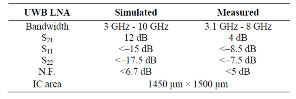
Table 1. Summary of simulated and measured RF characterizations in the UWB LNA.
inter-stage matching network associated with band-pass filter as input stage matching, which played bandwidthextension in this work. The UWB LNA circuit layout was achieved by the co-planar waveguide (CPW) topology, which was performed with the 0.15 μm D-mode pHEMT technology. The measured results revealed that a flatness power gain and low noise figure were obtained, which presented a constant gain of 4 dB and minimum noise figure of 3 dB in a frequency range of 3 GHz to 8 GHz, respectively.
In summary, the characterization of the proposed UWB LNA MMIC demonstrated wide bandwidth and an excellent noise characterization. The inductive peaking method with GaAs pHEMT technology exhibited the favorable RF characteristics, which was well suitable to fulfill extension wideband and low noise performance simultaneously.
5. Acknowledgements
The authors are grateful for the supporting in the Department of Electronic Engineering Vanung University and also thank to National Central University for noise figure measurement. Additional thanks extend to the WIN Semiconductors Corp. for circuit fabrication.
REFERENCES
- WPAN High Rate Alternative PHY Task Group 3a (TG3a), IEEE 802.15, 2007. http://www.ieee802.org/15/pub/TG3a.html
- G. R. Aiello and G. D. Rogerson, “Ultra-Wideband Wireless Systems,” IEEE Microwave Magazine, Vol. 4, No. 2, 2003, pp. 36-47. doi:10.1109/MMW.2003.1201597
- Y.-J. Lin, S. S. H. Hsu, J.-D. Jin and C. Y. Chan, “A 3.1 - 10.6 GHz Ultra-Wideband CMOS Low Noise Amplifier with Current-Reused Technique,” IEEE Microwave and Wireless Components Letters, Vol. 17, No. 3, 2007, pp. 232-234. doi:10.1109/LMWC.2006.890503
- C.-F. Liao and S.-I. Liu, “A Broadband Noise—Canceling CMOS LNA for 3.1 - 10.6-GHz UWB Receivers,” IEEE Journal of Solid-State Circuits, Vol. 42, No. 2, 2007, pp. 329-339. doi:10.1109/JSSC.2006.889356
- A. Bevilacqua and A. M. Niknejad, “An Ultra-Wideband CMOS LNA for 3.1 to 10.6 GHz Wireless Receiver,” IEEE Solid-State Circuits Conference (ISSCC) Digest of Technical Papers, Vol. 39, No. 12, 2004, pp. 382-383.
- C.-H. Wu, C.-H. Lee, W.-S. Chen and S.-I. Liu,“CMOS Wideband Amplifiers Using Multiple Inductive-Series Peaking Technigue,” IEEE Journal of Solid-State Circuits, Vol. 40, No. 2, 2005, pp. 548-552. doi:10.1109/JSSC.2004.840979
- S. Shekhar, X. Li, and D. J. Allstot, “A CMOS 3.1 - 10.6 GHz UWB LNA Employing Stagger-Compensated Series Peaking,” Radio Frequency Integrated Circuits (RFIC) Symposium, San Francisco, 2006, pp. 63-66.