World Journal of Mechanics
Vol. 1 No. 5 (2011) , Article ID: 8163 , 9 pages DOI:10.4236/wjm.2011.15031
Acousto-Diffusive Waves in a Piezoelectric-Semiconductor-Piezoelectric Sandwich Structure
1Department of Mathematics, National Institute of Technology, Hamirpur, India
2Department of Physics, National Institute of Technology, Hamirpur, India
E-mail: jns@nitham.ac.in, kks@nitham.ac.in, puri_nit@yahoo.com
Received July 12, 2011; revised August 13, 2011; accepted August 28, 2011
Keywords: Acousto-diffusive, Sandwich structure, Halfspace, Piezoelectricity
ABSTRACT
The propagation of acoustic waves in a homogeneous isotropic semiconducting layer sandwiched between two homogeneous transversely isotropic piezoelectric halfspaces has been investigated. The mathematical model of the problem is depicted by a set of partial differential equations of motion, Gauss equation in piezoelectric material and electron diffusion equation in semiconductor along with the boundary conditions to be satisfied at the piezoelectric-semiconductor interfaces. The secular equations describing the symmetric and asymmetric modes of wave propagation have been derived in compact form after obtaining the analytical expressions for various field quantities that govern the wave motion. The complex secular equation has been solved numerically using functional interaction method along with irreducible cardano method. The computer simulated results are obtained with the help of MATLAB software for 6mm cadmium selenide (CdSe) piezoelectric material and n-type silicon (Si) semiconductor in respect of dispersion curve, attenuation and specific loss factor of energy dissipation for symmetric (sym) and asymmetric (asym) modes of wave propagation. The study may find applications in non-destructive testing, resonators, waveguides etc.
1. Introduction
Lord Rayleigh [1] was the first who described the surface acoustic waves in connections with earthquake problems. Love [2] gave the first comprehensive treatment of dispersion for Rayleigh and Love waves in case of an elastic halfspace covered with a single solid layer. Bleustein [3] and Gulyaev [4] theoretically predicted that a pure shear surface acoustic wave can be guided by the free surface of a piezoelectric halfspace. White [5] predicted that an acoustic wave propagating in a piezoelectric semiconductor can be amplified under the effect of a dc electric field. Collins et al. [6] observed strong interaction between the wave on the surface of piezoelectric crystal and the drifting carriers in the nearby semiconductor. Dietz et al. [7] explored the acoustoelectric amplification of acoustic waves in the composite of piezoelectric dielectric and non-piezoelectric semiconductor.
Kagan [8] considered the surface wave propagation in a piezoelectric crystal underlying a conducting layer. It is predicted that the electric field excited by the wave in crystal penetrates into the conducting layer. Jin et al. [9] studied the Lamb wave propagation in a metallic semiinfinite medium covered with piezoelectric layer. It is found that the dispersion curves are asymptotic to the transverse velocity of the piezoelectric layer with increasing wave number. Sharma and Pal [10] investigated the Lamb wave propagation in a transversely isotropic piezothermoelastic plate. Sharma et al. [11] have analyzed the propagation of surface waves in a piezoelectric halfspace coated with a semiconductor layer.
Wu and Zhu [12] studied the Lamb wave propagation in a plate bordered with inviscid liquid layers and found that the acoustic impedance approach is valid when the plate thickness is much smaller than the wavelength of transverse wave in the solid. Sharma and Pathania [13] studied thermoelastic waves in a homogeneous isotropic plate bordered with inviscid liquid layers. Sharma and Kumar [14] analyzed Lamb waves in micropolar thermoelastic solid plates immersed in liquid with varying temperature.
Sorokin [15] discussed the wave propagation of purely shear deformation in an unbounded sandwich plate composed of two identical isotropic skin plies and an isotropic core ply. Qiang et al. [16] analyzes the guided wave propagation in multilayered piezoelectric structures whose each layer is made of an arbitrarily anisotropic piezoelectric material. Hu et al. [17] have given an exact analysis of forced thickness-twist vibrations of multilayered piezoelectric plates. Su et al. discussed the Lamb wave for identification of damages in composite structures. Lu and Bhattacharya [18] considered the elastic wave propagation in a sandwich structure with two thin stiff face plates and a thick compliant core.
Sandwich structures found applications in many fields such as spacecraft, aircraft, automobiles, boats and ships. Keeping in view the wide range applications and above referred work an attempt is made to study the acoustic waves in a sandwich structure consisting of semiconducting layer between two piezoelectric halfspaces. The phase velocity, attenuation and specific loss factor of energy dissipation for acoustic and optical modes of wave propagation in case of symmetric and asymmetric modes of wave propagation, in a sandwiched structure have been computed numerically from analytically developed model. The effect of variation of semiconducting layer thickness on the considered wave fields has also been taken in account to show the wave guide nature of the thin layer composite structure.
2. Formulation of the Problem
We consider an n-type homogeneous isotropic semiconductor layer of thickness  sandwiched between two homogeneous transversely isotropic, piezoelectric halfspaces. We take the origin of Cartesian coordinate system
  at any point on the mid-plane of the semiconductor layer and z-axis along the thickness of the layer as shown in Figure 1. Obviously the piezoelectric semi-spaces are represented by
  and
and  and the semiconductor layer occupies the region
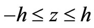 .
.
We choose x-axis along the direction of wave propa-
Figure 1. Geometry of the problem.
gation in such a way that all particles on the line parallel to y-axis are equally displaced. Thus all field quantities are independent of y-coordinate.
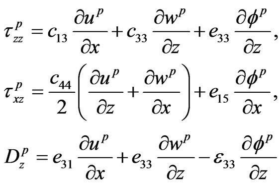
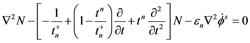
The basic governing equations of motion and electron diffusion for the composite structure under study, in the absence of body forces and electric sources, are given below:
1) Semiconductor (n-type) elastic layer (Sharma et al. [11]):
 (1)
(1)
 (2)
(2)
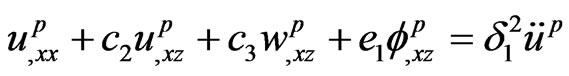
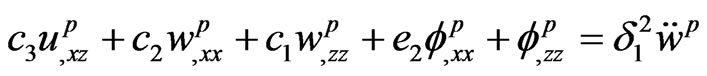
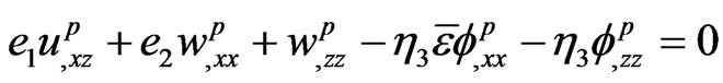
2) Piezoelectric  medium (Sharma et al. [11]):
 (3)
(3)
 (4)
(4)
 (5)
(5)
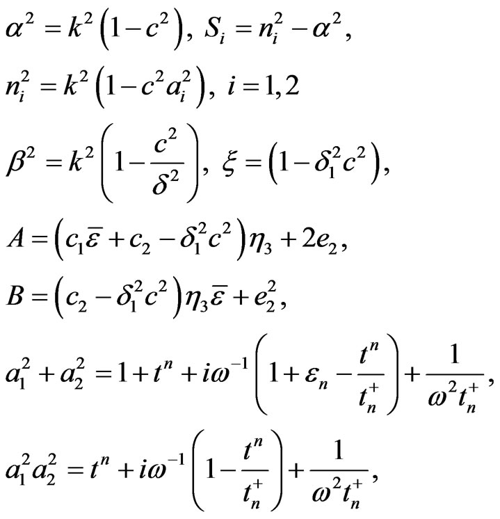
where the notations ,
,  ,
,  ,
, 
have been used. In the above equations the superposed dots on various quantities denote time differentiation and comma notation is used for spatial derivatives. Throughout this paper the superscripts  and
and  refer to piezoelectric and semiconductor materials, respectively. Here
  are Lamè’s parameters;
  is the density;
  is the elastodiffusive constants of electrons;
  is the diffusion coefficient of electron;
  and
and  respectively are the life and relaxation times of the carrier field;
  and
and  are the equilibrium and non-equilibrium values of electrons concentration;
  is the coefficient of linear thermal expansion of the semiconductor material. The quantities
  are flux-like constants and
  is the uniform temperature;
  and
and  are displacement vectors for semiconductor and piezoelectric materials, respectively. The quantities
 ,
, ,
, and
and are the electric potential, density, elastic parameters and piezoelectric constants;
  and
and  are the electric permittivity perpendicular and along the axis of symmetry of piezoelectric material, respectively.
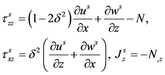
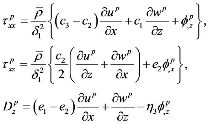
The non-vanishing components of stress tensor, current density and electric displacement in both the media are:
Semiconductor:
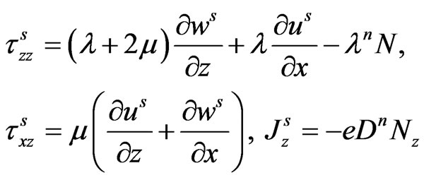 (6)
(6)
Piezoelectric:
 (7)
(7)
where  and
and  are the stress tensors. The quantities
  and
and  respectively denote the current density and carrier density gradient in semiconducting layer;
  is the electric displacement vector of piezoelectric material and
  is the electronic charge.
Boundary Conditions
The requirement of continuity of stresses, displacements, electric fields and current density at the interfaces  of two media leads to the following interfacial boundary conditions
 (8)
(8)
In order to simplify the model, we define following quantities
 (9)
(9)
where  is the characteristic frequency, and
 ,
,  are respectively, the longitudinal and shear wave velocities.
Introducing the quantities (9) in Equations (1) to (7), we obtain (on suppressing the primes for convenience)
 (10)
(10)
 (11)
(11)
 (12)
(12)
 (13)
(13)
 (14)
(14)
 (15)
(15)
 (16)
(16)
In order to facilitate the solution in semiconductor layer, we introduce the scalar and vector point potential functions  and
and  through the relations
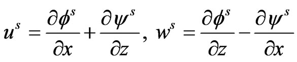 (17)
(17)
The equations (10)-(11) with the help of relations (17) provide us
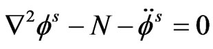 (18)
(18)
 (19)
(19)
 (20)
(20)
The equation (19) corresponds to purely transverse waves in the semiconductor which get decoupled from rest of the motion and is not affected by the concentration of charge carrier fields.
3. Formal Solution of the Problem
We take harmonic wave solution of the form
 (21)
(21)
where , here
 ,
,  and
and  are the non-dimensional phase velocity, angular frequency and wave number, respectively, in which primes have been suppressed for convenience.
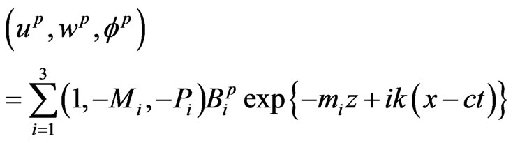
The use of solution (21) in equations (18)-(20) and (12)-(14) after straightforward algebraic reductions and simplifications leads to the formal solution satisfying the radiation conditions in semiconductor layer and piezoelectric as under:
 (22)
(22)
 (23)
(23)
for semiconductor layer 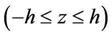
 (24)
(24)
for piezoelectric halfspace 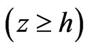 we have
 (25)
(25)
for piezoelectric halfspace  we have where
 (26)
(26)
 (27)
(27)
 (28)
(28)
 (29)
(29)
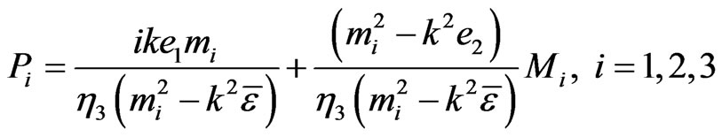
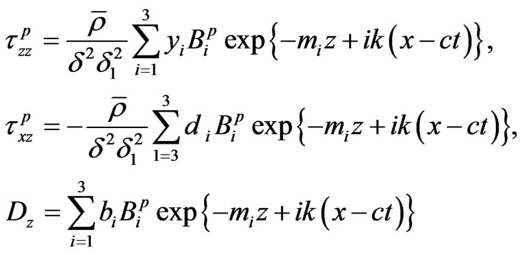
Consequently, the expressions for stresses, current density and displacements in the semiconductor layer are obtained from equations (15) and (17) via (22) and (23) as:
 (30)
(30)
 (31)
(31)
 (32)
(32)
 (33)
(33)
 (34)
(34)
where ,
,  ,
,  and
and  are the unknowns to be determine.
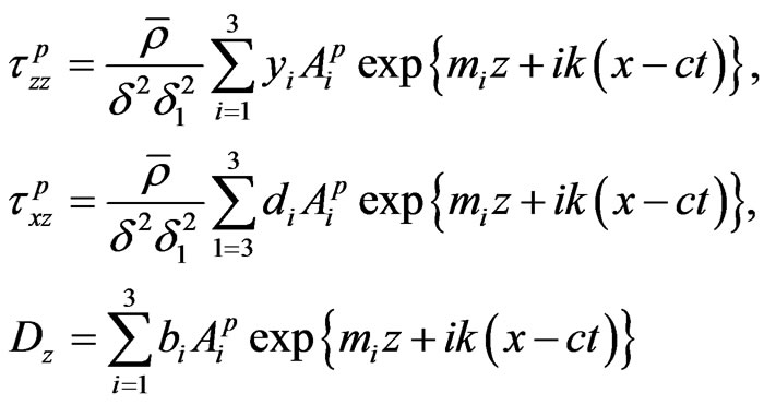
Using the solution (24) and (25) in Equation (16) we obtain the stresses and electric displacement as:
 (35)
(35)
for piezoelectric halfspace , and
, and
 (36)
(36)
for piezoelectric halfspace , where

 .
.
4. Secular Equation
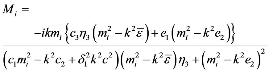
Upon imposing the boundary conditions (8) we obtain a coupled system of twelve homogeneous simultaneous algebraic equations in twelve unknowns  and
and  which has a non-trivial solution if the determinant of the coefficients
  vanishes. This requirement leads to a dispersion relation of the type
 (37)
(37)
where A, B, C and D are the  matrices whose non-zero elements are defined as below:
The non-zero elements  of matrix A are
The non-zero elements  of matrix B are
 ,
,  ,
,  ,
,
 ,
,  ,
,  ,
,
 ,
,  ,
,
 ,
,  ,
,
 ,
,  ,
,
 ,
,  ,
,
 ,
,  ,
,
The non-zero elements  of matrix C can be obtained from corresponding non-zero elements of
  of matrix B by replacing hyperbolic tangent function with the hyperbolic cotangent function and non-zero elements
  of matrix D are same as that of corresponding non-zero elements
  of matrix A. After some algebraic reductions and simplifications the secular equation (37) can be rewritten as:
 (38)
(38)
where
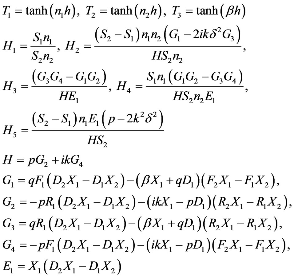 (39)
(39)
Here +1 stands for asymmetric mode of wave propagation and −1 for symmetric mode of wave propagation. The quantities  are defined as
 (40)
(40)
5. Solution of Secular Equation
In general, wave number and hence the phase velocities of the waves are complex quantities, therefore the waves are attenuated in space. In order to solve the secular equation (38), we take
 (41)
(41)
where ,
,  , and
, and  are real numbers.
Here, it may be noted that  and
and  respectively represent the phase velocity and attenuation coefficient of the waves. Using representation (41) in various relevant relations, the complex roots
  can be computed from Equations (27) with the help of Cardano method. The roots
  are further used to solve secular equation (38) to obtain phase velocity and attenuation coefficient of the surface waves by using function iteration numerical technique outlined below:
In general the secular equation (38) is of the form  which on using representation (41) leads to a system of two real equations
  and
and  . In order to apply functional iteration method we write
  and,
and,  where the functions
  and
and  are selected in such a way that they satisfy the conditions
 (42)
(42)
for all  in the neighborhood of the root. If
  be an initial approximation to root, then we can construct the successive approximations according to the formulae
 (43)
(43)
The sequence  of approximations to the root will converge to the actual root provided
  lies in the neighborhood of the actual root. For initial value of
 , the roots
  are computed from equations (27) by using Cardano method for each value of the non-dimensional wave number
  for assigned frequency. The values of
  so obtained are then used in secular Equation (38) to obtain the current values of
  and
and  each time which are further used to generate the sequence (43). The process is terminated as and when the condition
 ,
,  being arbitrarily small number to be selected at random to achieve the accuracy level, is satisfied. The procedure is continuously repeated for different values of non-dimensional wave number to obtain corresponding values of the phase velocity and attenuation coefficient. Thus, the real phase velocity and attenuation coefficient during the propagation of Rayleigh type waves in the composite structure under study can be computed from dispersion relation (38).
5.1. Specific Loss
The specific loss is the direct method of defining the internal friction for a material. According to Kolsky [19], in case of sinusoidal plane wave of small amplitude, the specific loss  equals to
  times the ratio of absolute value of the imaginary part of
  to the real part of
 , i.e.
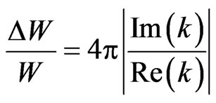 , where
  is a complex num-ber such that
 . Here
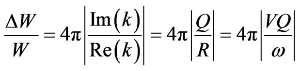 (44)
(44)
6. Numerical Results and Discussion
In this section we present the discussion of the results obtained through computer simulations from the analytical developments in the previous sections for a sandwich structure consisting of n-type silicon  layer and cadmium selenide
  halfspaces, whose material parameters and constants are defined as [11]:
1) Piezoelectric halfspace:
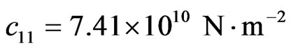 ,
,  ,
, 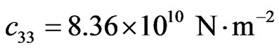 ,
,  ,
,  ,
,  ,
,  ,
,  ,
,
 ,
, .
.
2) Semiconductor layer:
 ,
,  ,
,  ,
,  ,
,  ,
, .
.
The numerical computations have been performed with the help of MATLAB software employing the procedure outlined in section 5 for the first two symmetric (sym) and asymmetric (asym) modes  of wave propagation. Here the quantity
  denotes the non-dimensional wave number of acoustic waves traveling in the semiconducting layer sandwiched between piezoelectric halfspaces.
From Figure 2 it is observed that phase velocity profiles of symmetric and asymmetric modes both, acoustic and optical, have significantly large magnitudes at small wave numbers (long wavelengths) which decrease with decreasing wavelengths and ultimately become stable and steady at extremely short wavelengths. The magnitude of phase velocity is small in case of fundamental (acoustic) modes but large for higher (optical) modes in the considered structure. This is attributed to the fact that
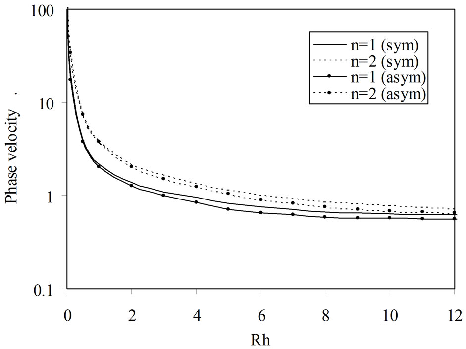
Figure 2. Variations of phase velocity versus wave number (Rh).
sat higher frequencies (short wavelengths), the semiconductor material layer behave like a thick slab and hence coupling between upper and lower interfaces is reduced as a result the properties of symmetric and asymmetric modes become almost similar. Under such situations the wave motion at the upper interface is not confined to the lower interface and displacement becomes localized near the respective boundaries and as a result the wave dispersion curves asymptotically approach to that of Rayleigh surface wave in case of acoustic modes and to shear wave velocity for optical modes in semiconductor material.
Moreover, the unbounded displacement field is characterized by the singularities of circular tangent functions. It is also observed that the coupling effect of various interacting fields decreases with increasing thickness of the semiconductor layer resulting in lower phase velocity as the wave travel along the interface (guided surface) with little disturbance to the semiconductor layer. The phase velocity of various modes at long wavelengths is noticed to be quite high because such waves penetrate deep in to the medium thereby creating significant disturbance in either of the material components because various interacting field become operative and contribute in increasing the magnitude of the phase velocity. Moreover, at long wavelengths the semiconductor layer behaves like a thin structure and hence its properties are greatly influenced by the substrate piezoelectric material under such situation through the interfaces which also attribute in high magnitude of phase velocity.
Figure 3 shows the variations of attenuation coefficient with the wave number. The attenuation of acoustic and optical modes of wave propagation increases in the range . It is evident that in this region attenuation observed sharp increase in contrast to the phase velocity profiles which show sharp decrease. The attenu-
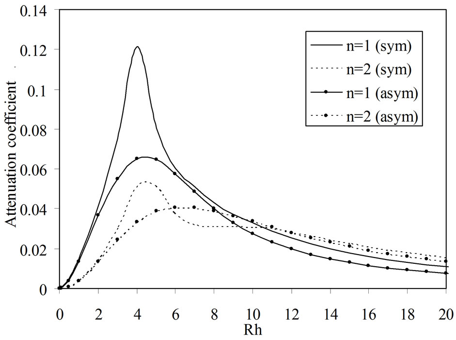
Figure 3. Variations of attenuation coefficient versus wave number (Rh).
ation of both acoustic and optical modes decreases before it attains a steady state for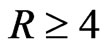 . It is attributed to the fact that large wavelength waves interact with the medium in contact to the maximum extent in contrast to that at short wavelengths in which case these follow the surface without significantly disturbing the medium. Thus the medium offer a high resistance to wave propagation at long wavelengths as compared to that at short wavelengths. At large wavelengths optical modes of wave propagation possess small value of attenuation as compared to that of acoustic modes; however the trend gets reversed at small wavelengths. The optical modes both symmetric and asymmetric possess higher attenuation.
Figure 4 presents the variations of specific loss factor of energy dissipation versus wave number. The specific loss factor follows the same trend as that of attenuation coefficient with the exception that it has higher magnitude than attenuation coefficient. This shows that at long wavelengths the medium offers high internal friction as compared to that at short wavelengths.
Figure 5 reveals that the phase velocity of both for symmetric and asymmetric modes increases with decreasing thickness of the semiconductor layer. Phase velocity possesses high magnitude when the semiconducting layer is thin. From Figures 6 and 7, it is evident that the attenuation and specific loss factor of energy dissipation have minimum magnitudes in case of thin semiconductor layer while the phase velocity has maximum magnitude. The magnitudes of attenuation and specific loss factor increase with increasing thickness of the semiconducting layer.
The increase of phase velocity with decreasing thickness of the semiconductor layer shows that the thin sandwiched layer acts like an acoustic waveguide. Acoustic waveguide confine the acoustic energy in the bulk of the
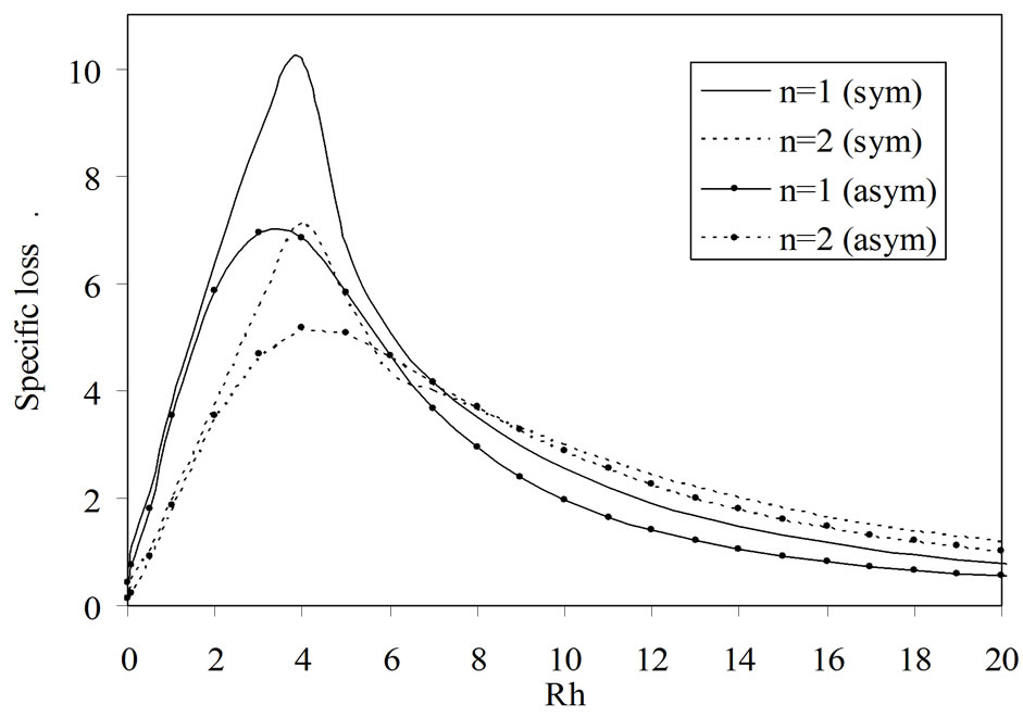
Figure 4. Variations of specific loss versus wave number (Rh).
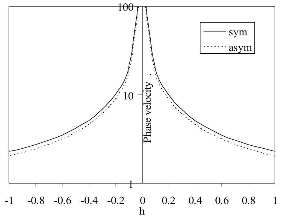
Figure 5. Variations of phase velocity versus layer thickness (h).
Figure 6. Variations of attenuation coefficient versus layer thickness (h).
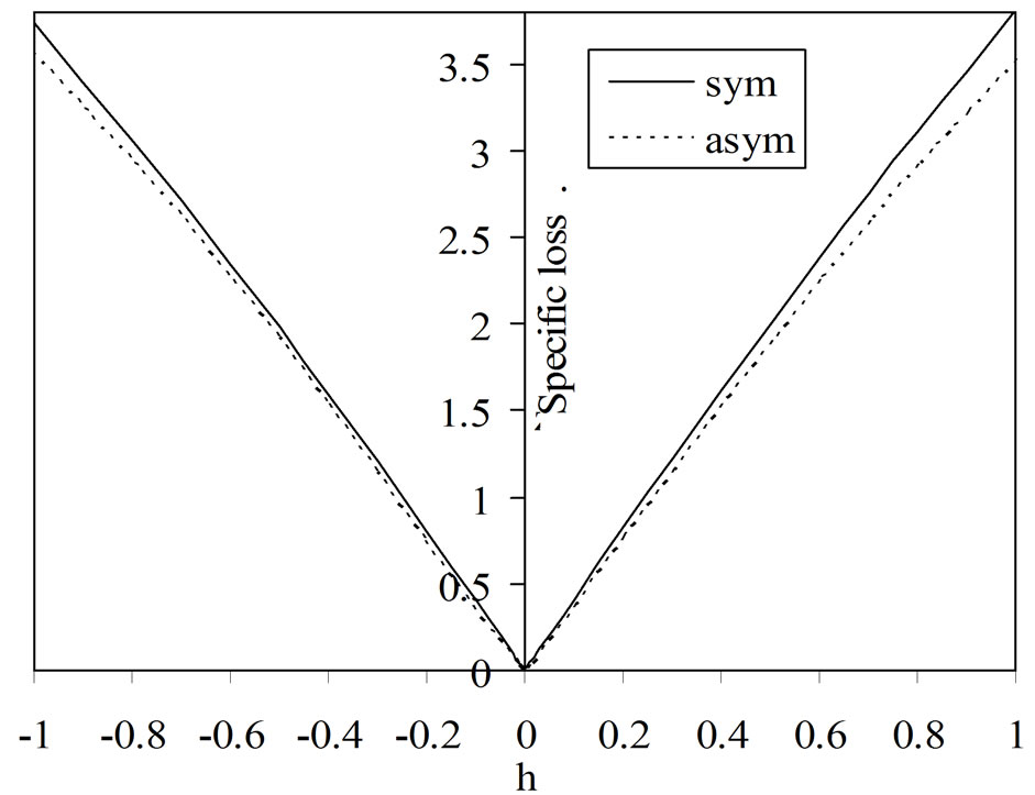
Figure 7. Variations of specific loss versus layer thickness (h).
layer through multiple reflections from the top and bottom interface as wave propagates and it generates a particle displacement at both the interfaces to ensure the channelized flow of energy through the waveguide.
7. Concluding Remarks
1) Functional iteration numerical technique along with Cardano method has been successfully used to solve the complex secular equation in order to compute the phase velocities, attenuation coefficients and specific loss factors of energy dissipation for different symmetric and asymmetric modes of wave propagation in a sandwich piezoelectric-semiconductor  structure.
2) Optical modes possess higher phase velocities than that of acoustic modes in symmetric as well as asymmetric mode of wave propagation.
3) Phase velocity profiles show dispersive character and decrease with the increasing wave number to become smooth and stable at short wavelengths.
4) The attenuation and specific loss factor increase with increasing wave number initially and then decrease after attaining maximum value in each case.
5) At large wavelengths acoustic modes possess high attenuation and specific loss factor of energy dissipation and reverse trends are noticed at small wavelengths.
6) Phase velocity increases with decreasing thickness of semiconducting layer while attenuation and specific loss factor of energy dissipation increase with the thickness of the layer showing a waveguide nature of the thin sandwiched semiconductor layer.
7) The study may find applications in fabrication of micro-electromechanical surface acoustic wave devices.
8. Acknowledgements
The authors are thankful to the reviewer for his useful suggestions for the improvement of this work. The author (JNS) thankfully acknowledges the financial support provided by CSIR, New Delhi via project grant No: 025(0184) EMR-II.
REFERENCES
- L. Rayleigh, “On Waves Propagated along the Plane Surface of Elastic Solids,” Proceedings of the London Mathematical Society, Vol. 17, No. 1, 1885, pp. 4-11. doi:10.1112/plms/s1-17.1.4
- A. E. H. Love, “Some Problems of Geodynamics,” Cambridge University Press, London, 1911.
- J. L. Bleustein, “A New Surface Wave in Piezoelectric Materials,” Applied Physics Letter, Vol. 13, 1968, p. 414. doi:10.1063/1.1652495
- Y. V. Gulyaev, “Electroacoustic Surface Waves in Solids,” Soviet Physics JETP, Vol. 9, 1969, pp. 37-38.
- D. L. White, “Amplification of Ultrasonic Waves in Piezoelectric Semiconductors,” Journal of Applied Physics, Vol. 33, 1962, pp. 2547-2554. doi:10.1063/1.1729015
- J. H. Collins, K. M. Lakin, C. F. Quate and H. J. Shaw, “Amplification of Acoustic Surface Waves with Adjacent Semiconductor and Piezoelectric Crystals,” Applied Physics Letter, Vol. 13, 1968, pp. 314-316. doi:10.1063/1.1652628
- D. R. Dietz, L. J. Busse and M. J. Fife, “Acoustoelectric Detection of Ultrasound Power with Composite Piezoelectric and Semiconductor Devices,” IEEE Transactions on Ultrasonics, Ferroelectrics and Frequency Control, Vol. 35, No. 2, 1988, pp. 146-151. doi:10.1109/58.4164
- V. D. Kagan, “Propagation of a Surface Acoustic Wave in a Layered System Containing a Two Dimensional Conducting Layer,” Semiconductors, Vol. 31, No. 4, 1997, pp. 407-410. doi:10.1134/1.1187321
- J. Jin, Q. Wang and S. T. Quek, “Lamb Wave Propagation in a Metallic Semi-Infinite Medium Covered with Piezoelectric Layer,” International Journal of Solids Structures, Vol. 39, No. 9, 2002, pp. 2547-2556. doi:10.1016/S0020-7683(02)00091-4
- J. N. Sharma and M. Pal, “Propagation of Lamb Waves in a Transversely Isotropic Piezothermoelastic Plates,” Jour nal of Sound and Vibration, Vol. 270, No. 4-5, 2004, pp. 587-610. doi:10.1016/S0022-460X(03)00093-2
- J. N. Sharma, K. K. Sharma and A. Kumar, “Surface Waves in a Piezoelectric-Semiconductor Composite Structures,” International Journal of Solids and Structures, Vol. 47, No. 6, 2010, pp. 816-826. doi:10.1016/j.ijsolstr.2009.11.016
- J. Wu and Z. Zhu, “The Propagation of Lamb Waves in a Plate Bordered with Layers of a Liquid,” Journal of the Acoustical Society of America, Vol. 91, 1992, pp. 861- 867. doi:10.1121/1.402491
- J. N. Sharma and Vijayata Pathania, “Generalized Thermoelastic Waves in Anisotropic Plates Sandwiched between Liquid Layers,” Journal of Sound and Vibration, Vol. 278, No. 1-2, 2006, pp. 383-411. doi:10.1016/j.jsv.2003.10.010
- J. N. Sharma and S. Kumar, “Lamb Waves in Micropolar Thermoelastic Solid Plates Immersed in Liquid with Varying Temperature,” Meccanica, Vol. 44, No. 3, 2009, pp. 305-319. doi:10.1007/s11012-008-9170-2
- S. V. Sorokin, “Analysis of Propagation of Waves of Purely Shear Deformation in a Sandwich Plate,” Journal of Sound and Vibration, Vol. 291, No. 3-5, 2006, pp. 1208-1220. doi:10.1016/j.jsv.2005.06.023
- G. Y. Qiang, C. W. Qiu and Z. Y. Liang, “Guided Wave Propagation in Multilayer Piezoelectric Structures,” Science in China Series G: Physics, Mechanics and Astronomy, Vol. 52, No. 7, 2009, pp. 1094-1104. doi:10.1007/s11433-009-0130-1
- H. P. Hu, Z. G. Chen, J. S. Yang and Y. T. Hu, “An Exact Analysis of Forced Thickness-Twist Vibrations of MultiLayered Piezoelectric Plates,” Acta Mechanica Solida Sinica, Vol. 20, No. 3, 2007, pp. 211-218.
- L. Liu and K. Bhattacharya, “Wave Propagation in a Sandwich Structure,” International Journal of Solids and Structures, Vol. 46, No. 17, 2009, pp. 3290-3300. doi:10.1016/j.ijsolstr.2009.04.023
- H. Kolsky, “Stress Waves in Solids,” Dover Press, New York, 1963.