Journal of Electronics Cooling and Thermal Control
Vol.4 No.1(2014), Article ID:43694,10 pages DOI:10.4236/jectc.2014.41005
Thermophotovoltaic Emitters Based on a One-Dimensional Metallic-Dielectric Multilayer Nanostructures
Samah G. Babiker1,2, Shuai Yong1*, Mohamed O. Sid-Ahmed3, Xie Ming1
1Department of Engineering Thermophysics, School of Energy Science and Engineering Harbin Institute of Technology, Harbin, China
2Department of Physics, Faculty of Education, University of the Holy Quran and Islamic Science, Omdurman, Sudan
3Department of Physics, Faculty of Sciences, Sudan University of Science and Technology, Khartoum, Sudan
Email: *shuaiyong@hit.edu.cn
Copyright © 2014 by authors and Scientific Research Publishing Inc.
This work is licensed under the Creative Commons Attribution International License (CC BY).
http://creativecommons.org/licenses/by/4.0/


Received 30 January 2014; revised 24 February 2014; accepted 3 March 2014
Abstract
In this paper, a one-dimensional multilayer is optimized for potential applications as thermophotovoltaic (TPV) selective emitter. The proposed TPV emitter was fabricated through a magnetron sputtering process by using the radio frequency (RF) magnetron sputtering system. The spectral emittance of the proposed TPV emitter is measured by using spectral transmittance and reflectance measurement system at wavelength from 0.3 μm to 2.5 μm at near-normal incident 8˚. The bidirectional reflectance distribution function BRDF is measured by three axis automated scatterometer (TAAS). The effect of the diffraction orders and plane of incidence on the spectral emittance of the proposed TPV emitter is calculated numerically by using the rigorous coupled-wave analysis (RCWA). The emittance spectrum of the proposed TPV selective emitter shows three close to unity emission peaks which are explained by the surface plasmon polariton (SPP), gap plasmon polariton (GPP) and magnetic polariton (MP) excitation. The results show that the proposed emitter has high emittance value in the spectral range of 0.69 < λ <1.97 μm and low reflectance distribution BRDF·cosθ value. It also has multi-reflection points and it works as a mirror. The measured results are in good agreement with the simulation results. The results show that the proposed TPV emitter, if used as a selective emitter with a low band gap photovoltaic cell (GaSb), would lead to high TPV overall efficiency and high electrical output power.
Keywords
Thermophotovoltaic; Selective Emitter; Rigorous Coupled Wave Analysis (RCWA); A Magnetron Sputtering Process; Spectral Emittance

1. Introduction
The depleting fossil fuel reserves encourage us to look for solutions such as new sources of energy, high energy conversion efficiency and recycling of waste heat by using of alternative energy sources. Thermophotovoltaic (TPV) systems provide a viable solution for fulfilling these requirements [1] [2] . Thermophotovoltaic (TPV) systems are capable of converting thermal infrared radiation directly into electricity by using photovoltaic effect [1] -[5] . The concept of TPV dates back to 1960s. It was only in recent years that technological improvements in the field of low band gap (0.50 - 0.75 eV) photovoltaic cells such as GaSb, GaInAs and GaInAsSb cells and high temperature selective emitting materials, have evoked a renewed interest in TPV generation of electricity [1] [5] [6] . The TPV system consists of heat source and optical cavity which comprises of a thermal radiator (emitter), photovoltaic PV cell and the spectral control components. The spectral control components are often classified in two types, cold-side and hot-side components. The cold-side components operate near room temperature and are installed on the cold side of the gap in the TPV system near or on the TPV cell, such as filters or reflectors or anti-reflective coatings on the TPV cell. The hot-side components operate at elevated temperatures (at or close to emitter temperature). They are installed upon or integrated into the emitter and are often called selective emitters [7] . The TPV system promises to be a very clean efficient and quiet source of electrical power. It is portable, with no moving parts (so low maintenance), with high power density output and it uses a wide variety of energy sources. As a result, TPV system can be more commonly used in many applications such as remote electrical and thermal energy supplies and aerospace power applications [1] [2] [8] -[12] . It has a very good potential to be an alternative to traditional batteries. TPV can also be used in the solar energy field, by using solar radiation to heat the emitter [13] [14] . However, the most obvious drawbacks of TPV systems are their low throughput and poor conversion efficiency, due to a large amount of unusable radiation [1] [15] . A highly efficient TPV system demands the optimization of the output power and throughput. Recently near-field thermal radiation has been proposed to enhance the throughput and conversion efficiency by bringing the emitter and TPV cell in close proximity, [3] . The conversion efficiency can be improved by controlling the emission spectrum and directions. One possible solution to increase the conversion efficiency and output power is to apply microscale radiation principles in TPV systems. Micro/nanostructures emitter (a selective emitter) can enhance TPV conversion efficiency by reducing the losses due to spectral mismatch between the source and the cell (low bandgap photons and carrier thermalisation). The output power can be increased by using micro/nanostructures in the emitter and filter. This reduces the amount of unusable radiation [16] . The throughput can also be increased by using micro/nanostructures, because it reduces the distance between the emitter and the TPV cell to sub-wavelength dimensions [17] . There are basically two different types of emitters, namely broadband emitters such as blackbody (BB) and selective emitters which are characterized by strong emission at certain wavelengths. A TPV system uses an emitter, which is heated up by various energy sources to high temperatures, as a source of radiation for photovoltaic energy conversion [2] [18] . That means that a large amount of unusable electromagnetic radiation impinges on the photovoltaic cell (PV).
Recently, the periodic micro/nanostructures surfaces in one-two or three (1D-2D-3D) dimensional have been investigated as promising potential to selective TPV emitters. Wang and Zhang [2] used 1D tungsten trilayer grating/thin-film nanostructure as a selective TPV emitter. Chen and Zhang [17] proposed and demonstrated the potential of 1D complex grating as a selective TPV emitter whose emittance is enhanced by exciting surface polsmon polaritons (SPPs). Narayanaswamy and Chen [20] also studied 1D photonic crystal (PhC) as a selective TPV emitter. Heinzel et al. [21] fabricated 2D wavelength-selective emitters for the near-infrared spectral range. Pralle et al. [22] manufactured 2D gold gratings that can emit over selected wavelengths in the mid-infrared. Sai et al. [23] experimentally demonstrated 2D tungsten grating with a strong emission peak and high thermal stability over 1400 K. A 3D tungsten photonic crystal [24] and 3D metallic woodpile as a TPV emitter was recently fabricated with an efficiency which exceeds 32% [25] .
An ideal TPV emitter should have high emissivity, close to unity, corresponding to the spectral region where a TPV cell has high quantum efficiency and as low as possible emissivity outside that region. It also needs to be polarization-insensitive so that high emissivity for both transverse electric wave and transverse magnetic wave can be achieved.
In this paper, a 1D 5-layer microstructure made of tungsten and silicon dioxide SiO2 in the form of (W/SiO2/ W/SiO2/W) is proposed and fabricated to use as a wavelength-selective and polarization-insensitive TPV emitter. The radiative properties were calculated and measured by the rigorous coupled-wave analysis RCWA and the spectral transmittance and reflectance measurement system. The bidirectional distribution function BRDF was also measured by using three axis automated scatterometer system TAAS at room temperature. The effects of the diffraction order and plane of incidence on the spectral emittance were investigated numerically.
2. Numerical Method
Rigorous coupled-wave analysis RCWA method was used for analyzing the diffraction of electromagnetic waves by periodic gratings. It analyzes the diffraction problem by solving Maxwell’s equations accurately in each of the three regions (input, multilayer and output), based on Fourier expansion [26] . The diffraction efficiency for each diffraction order is calculated with incident wave properties, feature dimensions, and dielectric function of the materials. The dielectric function of the materials is expressed as , where n is the refractive index and k is the extinction coefficient. The accuracy of the solution computed depends solely upon the number of terms retained in space harmonic expansion of electromagnetic fields, which corresponds to the diffraction order. Figure 1 is a schematic of the proposed TPV emitter considered in this study. The proposed TPV emitter consisted of alternating 5-layer made of tungsten W and silicon dioxide SiO2 in form of (W/SiO2/ W/SiO2/W) and the entire structure was deposited on quartz substrate. The thickness of the layers were:
 ,
,  ,
,  ,
, . Those layers were deposited on a quartz substrate. Tungsten was chosen as the emitter material because it has high melting point and it withstands high temperatures. The wavelength-dependent dielectric optical constants of tungsten and silica were obtained from tabulated data in Ref [27] . Angle
  is the corresponding emission angle. The emittance was calculated indirectly from the reflectance, based on Kirchhoff’s law. The space along the z-axis was divided into seven regions, as illustrated in Figure 1. The incident radiation is assumed to be linearly polarized and can be characterized by the incident wavevector as
 (1)
(1)
where  being the wavelength in vacuum is the free-space wavevector. The wavevector in the region M and region VII, respectively can be expressed as
 (2a)
(2a)
 (2b)
(2b)
 (3)
(3)
The normalized electric field of incidence  can be expressed as:
 (4)
(4)
The normalized magnetic field in region I can be expressed as
 (5)
(5)
R is the reflected amplitude of the electric field.
The electric and magnetic field components in region M can be expressed as a Fourier series:
 (6)
(6)
 (7)
(7)
Figure 1. Schematic of the proposed a TPV emitter made of 1D 5-layer (W/SiO2).
where  and
and  are the normalized amplitude of the jth space-harmonic fields that satisfy Maxwell’s equation in each divided layer. The magnetic field components in region VII can be expressed as
 (8)
(8)
T is the transmitted amplitude of the electric fields.
3. Experiment Setup
The proposed TPV emitter 1D 5-layer W/SiO2 is prepared through a magnetron sputtering process. The radio frequency (RF) magnetron sputtering system (JGP450, Shenyang Co. Ltd.) was used to deposit a thin film from sputtering targets onto a substrate and to fabricate the emitter. The tungsten (W) and silicon dioxide (SiO2) were used as sputtering targets and quartz as the substrate. The sputtering power and pressure were kept at 100 W and 150 W for tungsten and silicon dioxide, respectively, and operation pressure . The base vacuum level was
 . The Ar flow rate was kept at 30 SCCM and controlled by a mass flow meter. A single W layer was deposited on quartz substrate for 1200 s, and a single SiO2 layer was deposited on it for 3600 s. Figure 2 illustrates the W and SiO2 sputtering targets after deposition onto a substrate.
The thickness of the sputtering targets which were deposited onto a substrate per unit time can be calculated by using the following equations:
W: (9)
(9)
SiO2: (10)
(10)
where y is the thickness of the layer per (nm) and x is the time of deposition per minute, time for SiO2 per hour.
The layers thicknesses are 60, 60, 20,400 and 1000 nm, yielding the deposited rates to be 0.2205 nm/s, 0.0588 nm/s, for both of the W and SiO2, respectively. Scanning electron microscope SEM was used for characterization of the surface topography and morphology of the selective TPV emitter. The sample, before SEM, was coated by a thin layer of conductive material (gold), as shown in Figure 3. Figure 4 shows SEM of the selective TPV emitter sample. The spectral transmittance and reflectance measurement system was employed to measure the spectral emittance indirectly from the spectral reflectance at wavelength  from 0.3 μm to 2.5 μm. The bidirectional reflectance distribution function BRDF is defined as the ratio of the reflected power to the incident power [28] . Three-axis automated scatterometer TAAS was used to measure BRDF of the TPV emitter sample
Figure 2. The deposited sputtering targets on a substrate W (left) and SiO2 (right).
Figure 3. The image of the proposed selective TPV emitter sample before SEM.
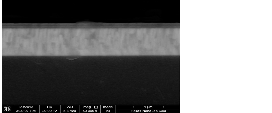
Figure 4. SEM image of the proposed selective TPV emitter sample.
at normal incident and  for both of the TE and TM polarization. It was also used to measure the BRFD at different incidence angles for TM polarization. The measured results were compared with the simulation results those obtained by RCWA method.
4. Results and Discussion
4.1. Emittance Measurements for the Proposed TPV Emitter
The spectral emittance of the proposed TPV emitter is measured by using spectral transmittance and reflectance measurement system at wavelength  from 0.3 μm to 2.5 μm and near normal incident 8˚. The spectral emittance of the TPV emitter is shown in Figure 5 which is calculated indirectly from the measured spectral reflectance. The spectral emittance of the plain tungsten is also shown in the figure for comparison. The results show three emissivity peaks close to unity, occurring in the wavelength range higher than 0.5 μm, while the spectral emittance at wavelengths shorter than 0.5 μm is much weaker, according to Planck’s blackbody spectral distribution.
The first peak at 0.81 μm occurs due to excitation of the surface plasmon polaritons (SPPs) at the air-tungsten interface. This is confirmed by polariton dispersion curves which depend on the relative permittivity or dielectric function (i.e. optical constants). The dispersion curve can be expressed as
 (11)
(11)
where  represents the frequency, c the light speed in vacuum, and
  the relative permittivity which corresponds to the optical constants of tungsten. The second peak at 1.13 μm is related to the interband absorption in tungsten which occurs due to gap plasmon polaritos (GPPs) excitation. A trilayer structure which forms a metal-dielectric-metal (W/SiO2/W) waveguide can support the propagation of the gap plasmon polaritons (GPPs) excitation. The third peak at 1.76 μm appears due to the magnetic plasmons (MPs) excitation that can be confirmed with electromagnetic field patterns. The 60-nm SiO2 spacer in region III is responsible for the variation where the MP is excited. The excitation of the MP mode can strongly localize the electromagnetic energy into the dielectric layer underneath the metal strip. The emissivity values at these peaks, obtained by measurements, are lower than those by simulation. This is could be attributed to the influence of the environment on the sample or due to the sample fabrication errors at preparation. This high spectral emissivity in the near IR (heat) is very suitable for TPV applications with a low band gap photovoltaic cell, such as GaSb. The measured results are very close to the simulation results. This sample has high emissivity, about 0.94, in our wavelength of interest, so it can be suitable to be used as a selective emitter. It can be seen, in the figure, that the emittance of the plain tungsten is not high enough at short wavelengths to meet the requirements for a good TPV emitter.
4.2. BRDF Measurements for the Proposed TPV Emitter
4.2.1. Effect of the Polarization on BRDF of the Proposed TPV Emitter
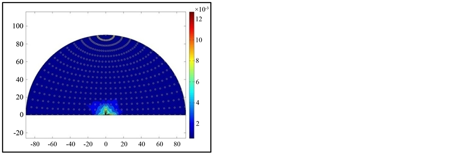
The reflectance distribution  in the half hemispherical space over the TPV emitter surface at normal incident,
  , is measured by using TAAS instrument for TE and TM polarization, respectively. The results are plotted in polar coordinates system (where the radial axis denotes zenith angle
  and the polar angle denotes the azimuthal angle
 ) as shown in Figure 6. The incident laser beam was focused on the sample at spot, which corresponds to the collimator diameter of about 5 mm and the blue color in the figure denotes the reflectance places. The results indicated that the TPV emitter has the same maximum value of
  of about
  for both of TE and TM polarization. The measured values of
  are very low and the accuracy is not expected be high. When the detector was positioned in front of the laser beam path, it blocks the laser beam and reflectance could not be obtained, because of the shadowing effect. The invalid data has been removed from the data set during post processing of the BRDF data. It is also noted that the reflected energy at the backward direction is greater than the forward for both of TE and TM polarization. The TPV emitter sample shows multi-reflection points and it works as a mirror. It also has a low
  value (high emittance value) which is desired for the performance of an ideal selective emitter. The high emittance increases the TPV overall efficiency and enhances the electrical output power, so the sample is suitable as a selective emitter.
4.2.2. Effect of the Plane of Incidence on BRDF of the Proposed TPV Emitter
The effect of the plane of incidence on the BRDF of the emitter is measured by using TAAS at different angles  and wavelength
  for TM wave. It can be seen from the results in Figure 7 that the maximum value of the reflectance distribution
  decreases as the incident angles
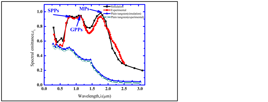
Figure 5. Measured and simulation ectral emittance of the proposed TPV selective emitter at near normal incident.
 (a)
(a)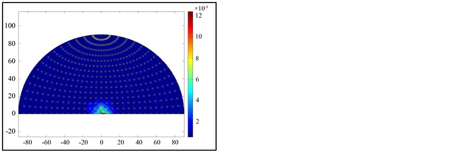 (b)
(b)
Figure 6. The  of the proposed TPV emitter at normal incident for (a) TE wave (b) TM wave.
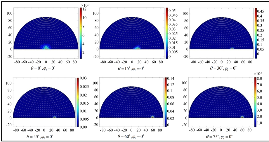
Figure 7. The  of the proposed TPV emitter at different incident angles in the polar coordinates for TM wave.
increase, except when . The maximum value measured of the reflectance distribution
  at
at  is very low compared with other incident angles; due to the detector blocking of the laser beam at this angle. The maximum value measured of the reflectance distribution
  is high and valid value at incident angle 30˚ and 60˚, due to the detector moves with rotation step of 6˚ for both
  and
and . The results explain the plane of incidence influence on the
  of the proposed TPV emitter. The proposed TPV emitter at normal incidence has a low reflectance distribution value and the certainty may not be high. To get more accurate data the laser beam should be incident on the proposed TPV emitter by angle higher than zero. The low reflectance distribution means that it has a high emittance value and this behavior is desired for the performance of an ideal selective emitter. Figure 8 shows the reflectance distribution
  in the incident plane at different incident angles all with
 . It can be noticed that at zenith angle
  and
and  the reflectance distribution
  has higher values compared to other angles at azimuthal angle
 , while it has lower value at
 .
.
4.3. Effect of the Diffraction Orders
The directional-hemispherical reflectance and transmittance can be obtained by summing up the diffraction efficiencies for all orders. When light impinges onto multilayer structure, it diffracts into different directions, depending on the wavelength and the layer period. The accuracy of the solution computed for emittance depends solely upon the number of the diffraction orders. The effect of the diffraction orders on the spectral emittance of the proposed TPV emitter was calculated numerically. The results in Figure 9 show that the diffraction orders (M) hardly have any effect on the emittance. Hence, M = 40 has been chosen in this study.
4.4. Effect of the Plane of Incidence
The effect of the plane of incidence (PoI) on the spectral emittance of the proposed TPV emitter was studied numerically at different incidence angles for TM wave, as shown in Figure 10. The results show that there is hardly any change in the first emittance peak, but the second emittance peak disappears while the third peak moves toward shorter wavelengths, when the angle of incidence is increased from 0˚ to 60˚. It appears that the proposed TPV emitter is insensitive to direction and has high emittance value in near Define abbreviations and acronyms the first time they are used in the text, even after they have been defined infrared region, so it can be suitable to be used as a wavelength selective emitter in TPV systems.
5. Conclusion
In order to enhance TPV overall efficiency and electrical output power, we proposed 1D 5-layer nanostructure TPV selective emitter. The spectral emittance and bidirectional reflectance distribution function BRDF of the proposed TPV emitter are experimentally measured. Three close-to-unity peaks on the emittance exist in the spectral emittance of the proposed TPV emitter in our spectral region of interest. They are explained by the
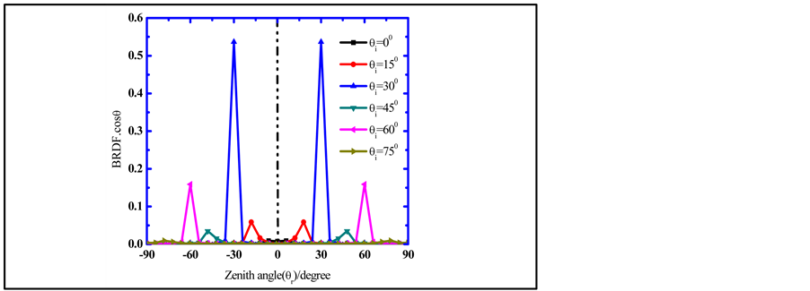
Figure 8. The  of the proposed TPV emitter incident plane at different incident angles all with
 .
.
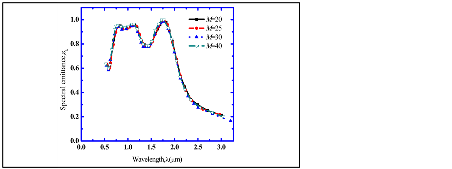
Figure 9. Spectral emittance with different diffraction orders for TM waves.
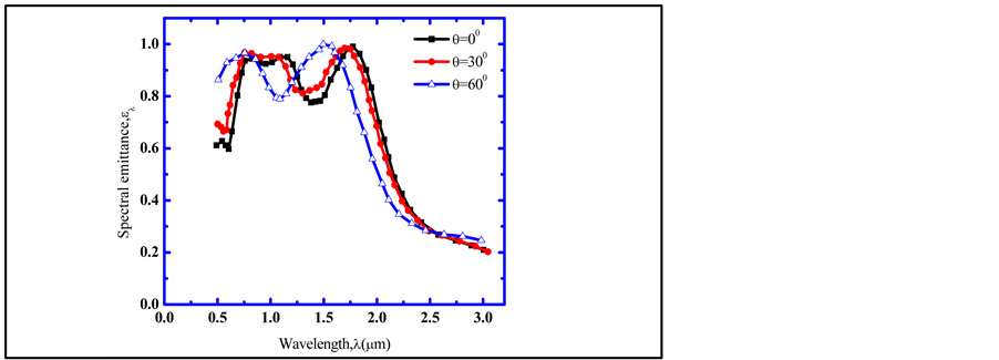
Figure 10. Spectral emittance at different incident angles for TM waves.
mechanisms of the SPPs, GPPs and MPs excitation. The measured results show that the proposed emitter has high reflectance distribution value  at zenith angle
 , while it has low value at
 . The maximum measured emittance value of the emitter is about 94% at wavelength 1.76 μm. The measured results are in good agreement with the simulation results. The performance of the proposed TPV emitter recommends it to be used in TPV applications, with GaSb cell (low band gap cell), as an efficient power generator.
Acknowledgements
This work is supported by the Foundation for Innovative Research Groups of the National Natural Science Foundation of China (No. 51276049) and the Fundamental Research Funds for the Central Universities (No. HIT. BRETIII.201227). A very special acknowledgement is made to the editors and referees whose constructive criticism has improved this paper.
References
- Basu, S., Chen, Y.-B. and Zhang, Z.M. (2007) Microscale Radiation in Thermophotovoltaic Devices: A Review. International Journal of Energy Research, 31, 689-716.
- Wang, L.P. and Zhang, Z.M. (2012) Wavelength-Selective and Diffuse Emitter Enhanced by Magnetic Polaritons for Thermophotovoltaics. Applied Physics Letters, 100, 063902(1-3).
- Park, K., Basu, S., King, W.P. and Zhang, Z.M. (2008) Performance Analysis of Near-Field Thermophotovoltaic Devices Considering Absorption Distribution. Journal of Quantitative Spectroscopy & Radiative Transfer, 109, 305-316. http://dx.doi.org/10.1016/j.jqsrt.2007.08.022
- Lal, N.N. and Blakers, A.W. (2009) Sliver Cells in Thermophotovoltaic Systems. Solar Energy Materials & Solar Cells, 93, 167-175. http://dx.doi.org/10.1016/j.solmat.2008.09.060
- Mostafa, S.I., Rafat, N.H. and El-Naggar, S.A. (2012) One-Dimensional Metallic-Dielectric (Ag/SiO2) Photonic Crystals Filter for Thermophotovoltaic Applications. Renewable Energy, 45, 245-250. http://dx.doi.org/10.1016/j.renene.2012.03.001
- Nefzaoui, E., Drevillon, J. and Joulain, K. (2012) Selective Emitters Design and Optimization for Thermophotovoltaic Applications. Applied Physics, 111, 084316. http://dx.doi.org/10.1063/1.4705363
- Jovanovic, N.Z. (2005) Two-Dimension Photonic Crystals as Selective Emitters for Thermophotovoltaic Power Conversion Applications. Ph.D. Thesis, Massachusetts Institute of Technology, Cambridge.
- Coutts, J.T. (1999) A Review of Progress in Thermophotovoltaic Generation of Electricity. Renewable and Sustainable Energy Reviews, 3, 177-184.
- Coutts, T.J. (2001) An Overview of Thermophotovoltaic Generation of Electricity. Solar Energy Materials & Solar Cells, 66, 443-452. http://dx.doi.org/10.1016/S0927-0248(00)00206-3
- Qiu, K. and Hayden, A.C.S. (2006) Development of a Silicon Concentrator Solar Cell Based TPV Power System. Energy Conversion and Management, 47, 365-376. http://dx.doi.org/10.1016/j.enconman.2005.04.008
- Mao, L. and Ye, H. (2010) New Development of One-Dimensional Si/SiO2 Photonic Crystals Filter for Thermophotovoltaic Applications. Renewable Energy, 35, 249-256. http://dx.doi.org/10.1016/j.renene.2009.06.013
- Wu, X., Ye, H. and Wang, J. (2011) Experimental Analysis of Cell Output Performance for a TPV System. Solar Energy Materials & Solar Cells, 95, 2459-2465. http://dx.doi.org/10.1016/j.solmat.2011.04.032
- Yimin, X., Xue, C. and Yuge, H. (2011) Design and Analysis of Solar Thermophotovoltaic Systems. Renewable Energy, 36, 374-387. http://dx.doi.org/10.1016/j.renene.2010.06.050
- Datas, A. and Algora, C. (2010) Detailed Balance Analysis of Solar Thermophotovoltaic Systems Made up of Single Junction Photovoltaic Cells and Broadband Thermal Emitters. Solar Energy Materials & Solar Cells, 94, 2137-2147. http://dx.doi.org/10.1016/j.solmat.2010.06.042
- Coutts, J.T., Guazzoni, G. and Luther, J. (2002) Thermophotovoltaic Generation of Electricity. Fifth Conference on Thermophotovoltaic Generation of Electricity, Rome, 16-19 September 2002.
- Chen, Y.-B. (2007) Rigorous Modeling of the Radiative Properties of Micro/Nanostructures and Comparisons with Measurements of Fabricated Gratings Slit Arrays. Ph.D. Thesis, Georgia Institute of Technology, Atlanta.
- Whale, M.D. (2001) The Influence of Interference and Heterojunctions on the Performance of Microscale Thermophotovoltaic Devices. Microscale Thermophysical Engineering, 5, 89-106. http://dx.doi.org/10.1080/108939501750397445
- Badescu, V. (2001) Thermodynamic Theory of Thermophotovoltaic Solar Energy Conversion. Applied Physics, 90, 6476-6486. http://dx.doi.org/10.1063/1.1415756
- Chen, Y.-B. and Zhang, Z.M. (2007) Design of Tungsten Complex Gratings for Thermophotovoltaic Radiators. Optics Communications, 269, 411-417. http://dx.doi.org/10.1016/j.optcom.2006.08.040
- Narayanaswamy, A. and Chen, G. (2004) Thermal Emission Control with One-Dimensional Metallodielectric Photonic Crystals. Physical Review, B70, 125101. http://dx.doi.org/10.1103/PhysRevB.70.125101
- Heinzel, A., Boerner, V., Gombert, A., Blasi, B., Wittwer, V. and Luther, J. (2000) Radiation Filters and Emitters for the NIR Based on Periodically Structured Metal Surfaces. Modern Optics, 47, 2399-2419. http://dx.doi.org/10.1080/09500340008230522
- Pralle, M.U., Moelders, N., McNeal, M.P., Puscasu, I., Greenwald, A.C., Daly, J.T. and Johnson, E.A. (2002) Photonic Crystal Enhanced Narrow-Band Infrared Emitters. Applied Physics Letters, 81, 4685-4687. http://dx.doi.org/10.1063/1.1526919
- Sai, H., Kanamori, Y. and Yugami, H. (2003) High-Temperature Resistive Surface Grating for Spectral Control of Thermal Radiation. Applied Physics Letters, 82, 1685-1687. http://dx.doi.org/10.1063/1.1560867
- Lin, Y.S., Moreno, J. and Fleming, J.G. (2003) Three-Dimensional Photonic-Crystal Emitter for Thermal Photovoltaic Power Generation. Applied Physics Letters, 83, 380-382. http://dx.doi.org/10.1063/1.1592614
- Nagpal, P., Han, S.E., Stein, A. and Norris, D.J. (2008) Efficient Low-Temperature Thermophotovoltaic Emitters from Metallic Photonic Crystals. Nano Letters, 8, 3238-3243. http://dx.doi.org/10.1021/nl801571z
- Peng, S. and Morris, G.M. (1995) Efficient Implementation of Rigorous Coupled-Wave Analysis for Surface-Relief Gratings. Journal of the Optical Society of America A, 12, 1087-1096. http://dx.doi.org/10.1364/JOSAA.12.001087
- Palik, E.D. (1998) Handbook of Optical Constants of Solids. Academic Press, San Diego.
- Shen, Y.J., Zhu, Q.Z. and Zhang, Z.M. (2003) A Scatterometer for Measuring the Bidirectional Reflectance and Transmittance of Semiconductor Wafers with Rough Surfaces. Review of Scientific Instruments, 74, 4885-4892. http://dx.doi.org/10.1063/1.1614853
NOTES

*Corresponding author.