 Journal of Modern Physics, 2011, 2, 341-349 doi:10.4236/jmp.2011.25042 Published Online May 2011 (http://www.SciRP.org/journal/jmp) Copyright © 2011 SciRes. JMP MOCVD of Molybdenum Sulphide Thin Film via Single Solid Source Precursor Bis-(Morpholinodithioato-s,s’)-Mo Bolutife Olofinjana1, Gabriel Egharevba2, Bidini Taleatu1, Olum id e Akinwunm i1, Ezekie l Oladele Ajayi1 1Department of Physics, Obafemi Awol ow o University, Ile- Ife, Nigeria 2Department of Chemistry , Obafemi Awolowo University, Ile-Ife, Nigeria E-mail: eajayi@oauife.edu.ng Received January 12, 2011; revised March 16, 20 1 1; acce pted April 7, 2011 Abstract A single solid source precursor bis-(morpholinodithioato-s,s’)-Mo was prepared and molybdenum sulphide thin film was deposited on sodalime glass using Metal Organic Chemical Vapour Deposition (MOCVD) technique at deposition temperature of 420˚C. The film was characterized using Rutherford Backscattering Spectroscopy (RBS), Ultraviolet-Visible Spectroscopy, Four-point Probe technique, Scanning Electron Mi- croscopy (SEM), X-ray Diffractometry (XRD) and Atomic Force Microscopy (AFM). A direct optical band gap of 1.77 eV was obtained from the analysis of the absorption spectrum. The sheet resistance was found to be of the order of 10–5 Ω–1·cm–1. SEM micrographs of the films showed the layered structure of the film with an estimated grain size that is less than 2 µm while XRD indicates parallel orientation of the basal plane to the substrate surface. Keywords: Molybdenum Sulphide, Precursor, Metal Organic Chemical Vapour Deposition (MOCVD), Thin Film, Characterization 1. Introduction Transition metal chalcogenides constitute an important class of functional materials that are prime candidates for the exploration of structure-property relationships in sol- ids. Subtle changes in shape, size and phase of these ma- terials result in variations in physical properties which can be exploited for various technological applications. This wide range of interesting technological applications has been the primary driving force behind much of the interest in these solid state compounds. Transition metal dichalcogenides (TMDC) have been widely studied [1-3]. These materials exhibit a wide range of electronic prop- erties ranging from insulating to conducting with evi- dence of superconductivity in some of the members of the class [4]. The unique characteristic of molybdenum disulphide, MoS2 is its highly anisotrop ic crystal layer structure. It is characterized by a lamellar structure which is similar to that of graphite [2]. Monolayers of Mo are sandwiched between monolayers of sulphur which are held together by relatively weak Van der Waals bonding between S-Mo-S layers. There is a strong covalent bonding within the sandwiches i.e. between molybdenum and sulphur atom. Each layer comprises of a layer of Mo atoms ar- ranged in hexagonal array situated between two hexago- nal layers of S atoms. Furthermore, the MoS2 layer struc- ture can exhibit two types of crystalline orientation, ei- ther the basal planes are parallel or perpendicular to the substrate. In contrast, MoS3 exist only in an amorphous form with short range order [5]. Molybdenum sulphide thin films have also found in- dustrial applications in the field of optical devices and electronics. These applications arise from their optical and electrical properties. They have band gaps (1.1 - 1.8 eV) well fitted to solar spectrum [6-8]. The direct and indirect gaps are derived from non bonding molecular orbital which leads to high corrosion resistance [9]. As a result, they are excellent candidates for efficient solar energy cells [10,11]. The layered structure of molybde- num sulphide enables weak Van der Waals interaction at the surface interface substantially relieving the lattice mismatch problem which leads to generation of disloca- tion at the interface that acts as minority carrier recom- bination centers detrimental to cell efficiency. Photo- voltaic applications of these materials have been sug- gested and encouraging results were obtained. However, Jamieson and Jakovidis (2004) [12] proposed that the  B. OLOFINJANA ET AL. 342 MoS2 thin films must be textured for an efficient hetero- junction photovoltaic cell. Ponomarev et al. (1998) [13] on the other hand concluded that MoS2 thin films are photoactive in which photoconductivity measurements reveal a direct band gap of 1.71 eV with Van der Waals planes parallel to substrate. Molybdenum sulphide thin films also have wide range of potential application as field emitters [14,15], ther- moelectric materials [16], catalyst [17], in electrochro- mic devices [18,19], and as cath ode in secondary lithium batteries [20-22]. The intercalation of lithium into mo- lybdenum sulphide produces a material that is highly useful in lithium ion batteries because of its ability to exchange lithium reversibly in non aqueous electrolytes. The amount of intercalated lithium and also the reversi- ble extracted lithium depend on the quality of MoS2 and their prior treatment [23]. Furthermore, Imanishi et al. (1992) [20] observed that the discharge and charge char- acteristics strongly depend on the lithium diffusion in the Van der Waals gap. Molybdenum sulphide thin films have been prepared by variety of techniques. Such techniques include spin coating [5,24], radio frequency (rf) sputtering [12,25,26], dc magnetron sputtering [27-31], dip coating [32], pulsed laser deposition and pulsed laser ab lation [33-35]. Oth ers include, electrodeposition [6,11,13], successive ionic layer adsorption and reaction (SILAR) [36], Chemical reaction technique [37], CVD [38-40] and so on. In the latter case, Schleich et al. (1989) [40] used molybdenum hexafluoride (MoF6) and Hexamethyldisulphide (HMDST) as precursors while Endler et al. (1999) [38] used MoCl5 and H2S as precursors. However, Cheon et al. (1997) [39] used a metal organic precursor tert-butyl thioate Mo (S-t-Bu)4 which is an air sensitive compound. The use of MOCVD technique has received much at- traction due to its great potential application to fabricate high quality films. Most of the other techniques have their different deficiencies ranging from non-uniformity of films to lack of reproducibility in composition of films with different levels of impurity. This is due to the fact that two or more precursor sources of different aerosol properties are used. In this work, we report the preparation of bis-(mor- pholinodithioato-s,s’)-Mo which is a single solid source precursor and the deposition of molybdenum sulphide thin films from this precursor through MOCVD method on sodalime glass substrate at deposition temperature of 420˚C. Compositional study; optical and electrical char- acterization; surface morphology, structure and rough- ness of the films are also reported. 2. Experimental 2.1. Precursor Preparation The single solid source precursor, bis-(morpholinodi- thioato-s,s’)-Mo was prepared using the procedure re- ported by Ajayi et al. (1994) [41]. This method has also been extended to cover ternary and quaternary sulphides [42,43]. The intermediate complex, ammonium mor- pholino-dithiocarbamate was prepared according to the method re po rt ed by Ajayi et al. (1994) [41]. Ammonium morpholino-dithiocarbamate (14.42 g, 0.08 mol) was dissolved in warm methanol (60 cm3) en- suring that the compound was completely dissolved. A so- lution of molybdenum(V) chloride, MoCl5 (10.93 g, 0.04 mol) in methanol (60 cm3), was then added dropwise to the solution of ammonium morpholino-dithiocarbamate in methanol while stiring vigorously on a hot plate. The product obtained as a precipitate was filtered off and later dried in a dessicator to yield 11.78 g (69.70% y ield). 2.2. Thin Film Deposition The thin film of molybdenum sulphide was prepared by the pyrolytic method of MOCVD which has been re- ported previously [44]. The substrate used was sodalime glass slides with composition O,Si,Na,Ca,Mg,Al = 60,25,10,3,1,1. The film was deposited at temperature of 420˚C. The set up for the depositi on is shown i n Figure 1. Figure 1. Apparatus for pyrolysis of the precursor. Copyright © 2011 SciRes. JMP 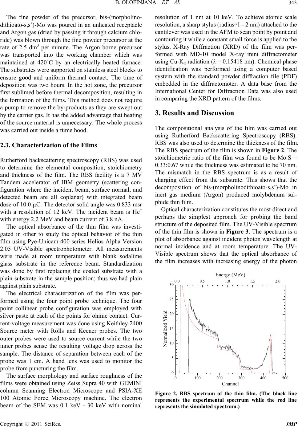 B. OLOFINJANA ET AL. Copyright © 2011 SciRes. JMP 343 The fine powder of the precursor, bis-(morpholino- dithioato-s,s’)-Mo was poured in an unheated receptacle and Argon gas (dried by passing it through calcium chlo- ride) was blown through the fine powder precursor at the rate of 2.5 dm3 per minute. The Argon borne precursor was transported into the working chamber which was maintained at 420˚C by an electrically heated furnace. The substrates were supported on stainless steel blocks to ensure good and uniform thermal contact. The time of deposition was two hours. In the hot zone, the precursor first sublimed before thermal decomposition, resulting in the formation of the films. This method does not require a pump to remove the by-products as they are swept out by the carrier gas. It has the added advantage that heating of the source material is unnecessary. The whole process was carried out inside a fume hood. 2.3. Characterization of the Films Rutherford backscattering spectroscopy (RBS) was used to determine the elemental composition, stoichiometry and thickness of the film. The RBS facility is a 7 MV Tandem accelerator of IBM geometry (scattering con- figuration where the incident beam, surface normal, and detected beam are all coplanar) with integrated beam dose of 10.0 µC. The detector solid angle was 0.833 msr with a resolution of 12 keV. The incident beam is He+ with energy 2.2 MeV and beam current of 3.8 nA. The optical absorbance of the thin film was investi- gated in other to study the optical behavior of the thin film using Pye-Unicam 400 series Helios Alpha Version 2.05 UV-Visible spectrophotometer. All measurements were made at room temperature with blank sodalime glass substrate in the reference beam. Standardization was done by first replacing the coated substrate with a plain substrate in the sample position; thus we had plain against plain subst rate . The electrical characterization of the film was per- formed using the four point probe technique. The four point collinear probe configuration was employed with silver paste at each of the points for ohmic contact. Cur- rent-voltage measurement was done using Keithley 2400 Source meter with Rolls and Keener probes. The two outer probes were used to source current while the two inner probes sense the resulting voltage drop across the sample. The distance of separation between each of the probe was 1 cm. A hand lens was used to monitor the probe from puncturing the film. The surface morphology and surface roughness of the films were obtained using Zeiss Supra 40 with GEMINI column Scanning Electron Microscope and PSIA-XE 100 Atomic Force Microscopy machine. The electron beam of the SEM was 0.1 keV - 30 keV with nominal resolution of 1 nm at 10 keV. To achieve atomic scale resolution, a sharp stylus (radius ̴ 1 - 2 nm) attached to the cantilever was used in the AFM to scan point by point and contouring it while a constant small force is applied to the stylus. X-Ray Diffraction (XRD) of the film was per- formed with MD-10 model X-ray mini diffractometer using Cu-Kα radiation (λ = 0.15418 nm). Chemical phase identification was performed using a computer based system with the standard powder diffraction file (PDF) embedded in the diffractomoter. A data base from the International Center for Diffraction Data was also used in comparing the XRD pattern of the films. 3. Results and Discussion The compositional analysis of the film was carried out using Rutherford Backscattering Spectroscopy (RBS). RBS was also used to determin e the thickness o f the film. The RBS spectrum of the film is shown in Figure 2. The stoichiometric ratio of the film was found to be Mo:S = 0.33:0.67 while the thickness was estimated to be 70 nm. The mismatch in the RBS spectrum is as a result of charging effect from the substrate. This shows that the decomposition of bis-(morpholinodithioato-s,s’)-Mo in inert gas medium (Argon) produced molybdenum sul- phide thin film. Optical characterization constitutes the most direct and perhaps the simplest approach for probing the band structure of the deposited film. The UV-Visible spectrum of the thin film is shown in Figure 3. The spectrum is a plot of absorbance against incident photon wavelength at normal incidence and at room temperature. The UV- Visible spectrum shows that the optical absorbance of the film increases with increasing energy of the photon 0100 200 300 400 500 Channel 0 5 10 15 20 25 30 Normalized Yield 0.0 0.5 1.0 1.5 2.0 Energy (MeV) Figure 2. RBS spectrum of the thin film. (The black line represents the experimental spectrum while the red line represents the simulated spectrum.) 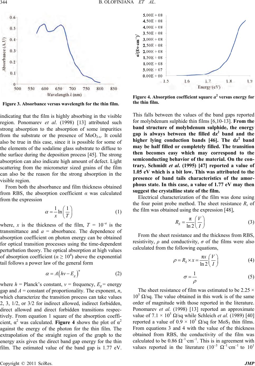 B. OLOFINJANA ET AL. 344 Figure 3. Absorbance versus wavelength for the thin film. indicating that the film is highly absorbing in the visible region. Ponomarev et al. (1998) [13] attributed such strong absorption to the absorption of some impurities from the substrate or the presence of MoO3-x. It could also be true in this case, since it is possible for some of the elements of the sodalime glass substrate to diffuse to the surface during the deposition process [45]. The strong absorption can also indicate high amount of defect. Light scattering from the micrometer sized grains of the film can also be the reason for the strong absorption in the visible region. From both the absorbance and film thickness obtained from RBS, the absorption coefficient α was calculated from the expression 11 ln T (1) where, x is the thickness of the film, T = 10–a is the transmittance and a = absorbance. The dependence of absorption coefficient on photon energy can be obtained for optical transition processes using the time-dependent perturbation theo ry. Th e optical ab so rp tio n at high valu es of absorption coefficient (α ≥ 104) above the exponential tail follows a power law of the general form n g Ahv E (2) where h = Planck’s constant, ν = frequency, Eg = energy gap and A = constant of proportionality. The expon ent, n, which characterize the transition process can take values 2, 3, 1/2, or 3/2 for indirect allowed, indirect forbidden, direct allowed and direct forbidden transitions respec- tively. From equation 1 square of the absorption coeffi- cient, α2 was calculated. Figure 4 shows the plot of α2 against the energy of the photon for the thin film. The extrapolation of the straight region of the graph to the energy axis gives the direct band gap energy for the thin film. The estimated value of the band gap is 1.77 eV. Figure 4. Absorption coefficient square α2 versus energy for the thin film. This falls between the values of the band gaps reported for molybdenum sulphide thin films [6,10-13]. From the band structure of molybdenum sulphide, the energy gap is always between the filled dz2 band and the higher lying conduction bands [46]. The dz2 band may be half filled or completely filled. The transition then becomes easy which may correspond to the semiconducting behavior of the material. On the con- trary, Schmidt et al. (1995) [47] reported a value of 1.05 eV which is a bit low. This was attributed to the presence of band tails characteristics of the amor- phous state. In this case, a value of 1.77 eV may then suggest the crystalline state of the film. Electrical characterization of the film was done using the four point probe method. The sheet resistance Rs of the film was obtained using the expression [48], π ln 2 SV R (3) From the sheet resistance and the thickness from RBS, resistivity, ρ and conductivity, σ of the films were also calculated from the following equations, π ln 2 S V Rx (4) 1 (5) The sheet resistance of film was estimated to be 2.25 × 10⁵ Ω/sq. The value obtained in this work is of the same order of magnitude with those reported in the literature. Ponomarev et al. (1998) [13] reported an approximate value of 7.1 × 10⁵ Ω/sq while Schleich et al. (1989) [40] reported a value of 0.9 × 10⁵ Ω/sq for MoS3 thin films. From equations 3 and 4 with the value of the thickness obtained from RBS, the conductivity of the film was calculated to be 0.86 Ω–1·cm–1. This is in agreement with values reported in the literature (10–3 Ω–1·cm–1 to 101 Copyright © 2011 SciRes. JMP 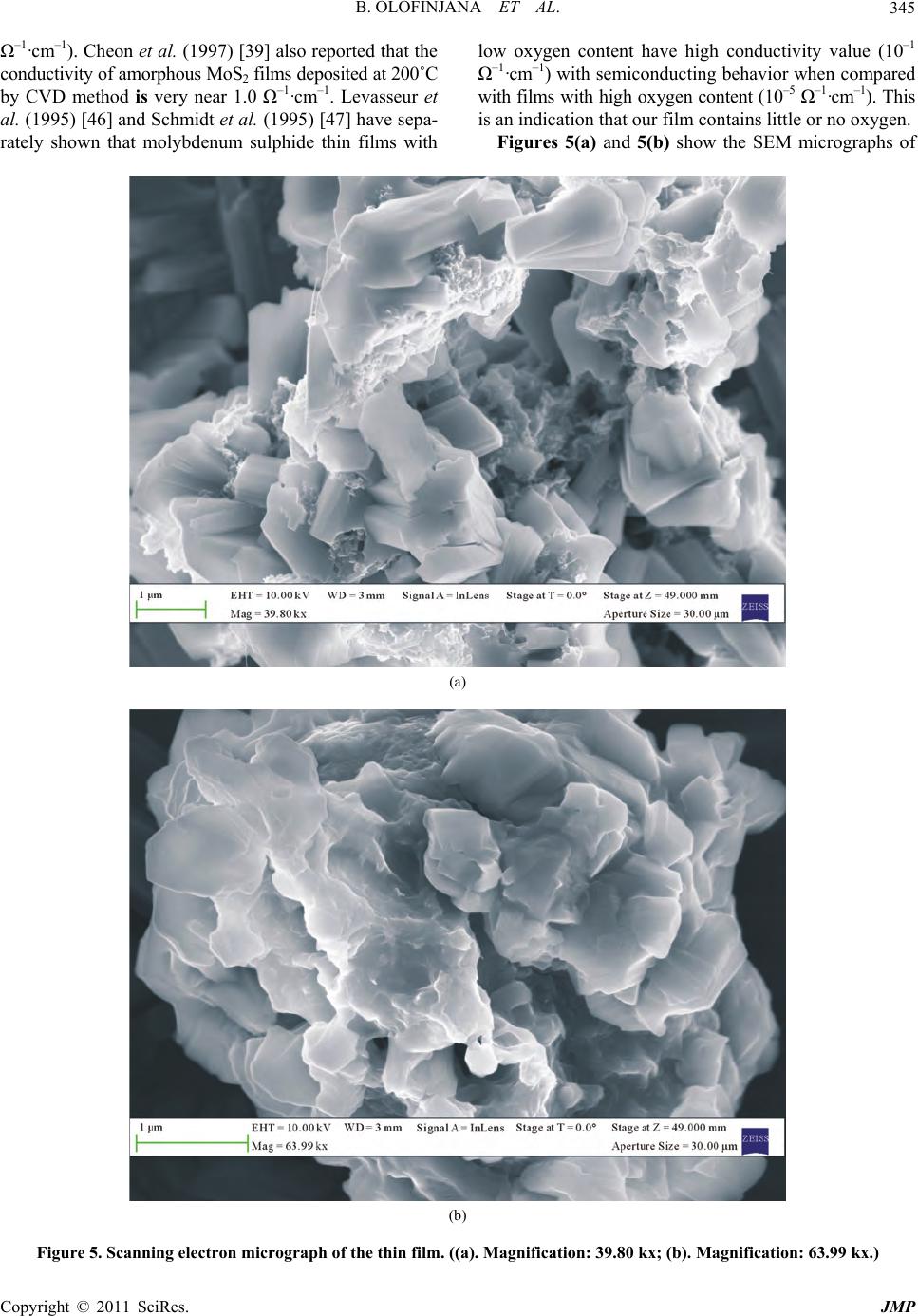 B. OLOFINJANA ET AL. Copyright © 2011 SciRes. JMP 345 Ω–1·cm–1). Cheon et al. (1997) [39] also reported th at the conductivity of amorphous MoS2 films deposited at 200˚C by CVD method is very near 1.0 Ω–1·cm–1. Levasseur et al. (1995) [46] and Schmidt et al. (1995) [47] have sepa- rately shown that molybdenum sulphide thin films with low oxygen content have high conductivity value (10–1 Ω–1·cm–1) with semiconducting behavior when compared with films with high oxygen content (10–5 Ω–1·cm–1). This is an indication that our film contains little or no oxygen. Figures 5(a) and 5(b) show the SEM micrographs of (a) (b) Figure 5. Scanning electron micrograph of the thin film. ((a). Magnification: 39.80 kx; (b). Magnification: 63.99 kx.) 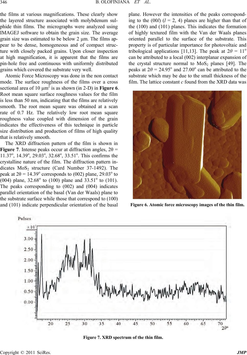 B. OLOFINJANA ET AL. Copyright © 2011 SciRes. JMP 346 the films at various magnifications. These clearly show the layered structure associated with molybdenum sul- phide thin films. The micrographs were analyzed using IMAGEJ software to obtain the grain size. The average grain size was estimated to be below 2 µm. The films ap- pear to be dense, homogeneous and of compact struc- ture with closely packed grains. Upon closer inspection at high magnification, it is apparent that the films are pin-hole free and continuous with uniformly distributed grains which covered the substrate very well. Atomic Force Microscopy was done in the non contact mode. The surface roughness of the films over a cross sectional area of 10 µm2 is as shown (in 2-D) in Figure 6. Root mean square surface roughness values for the film is less than 50 nm, indicating that the films are relatively smooth. The root mean square was obtained at a scan rate of 0.7 Hz. The relatively low root mean square roughness value coupled with dimension of the grain indicates the effectiveness of this technique in particle size distribution and production of films of high quality that is relatively smooth. The XRD diffraction pattern of the film is shown in Figure 7. Intense peaks occur at diffraction angles, 2θ = 11.37o, 14.39o, 29.03o, 32.68o, 33.51o. This confirms the crystalline nature of the film. The diffraction pattern in- dicates MoS2 structure (Card Number 37-1492). The peak at 2θ = 14.39o corresponds to (002) plane, 29.03o to (004) plane, 32.68o to (100) plane and 33.51o to (101). The peaks corresponding to (002) and (004) indicates parallel orientation of the basal (Van der Waals) plane to the substrate surface while those that correspond to (100) and (101) indicate perpendicular orientation of the basal plane. However the intensities of the peaks correspond- ing to the (00l) (l = 2, 4) planes are higher than that of the (100) and (101) planes. This indicates the formation of highly textured film with the Van der Waals planes oriented parallel to the surface of the substrate. This property is of particular importance for photovoltaic and tribological applications [11,13]. The peak at 2θ = 11o can be attributed to a local (002) interplanar expansion of the crystal structure normal to MoS2 planes [49]. The peaks at 2θ = 24.95o and 27.00o can be attributed to the substrate which may be due to the small thick ness of the film. The lattice constant c found from the XRD data was Figure 6. Atomic force microscopy images of the thin film. Figure 7. XRD spectrum of the thin film.  B. OLOFINJANA ET AL.347 found to be 12.31 Å. This value is approximately the same value (12.298 Å) reported in the literature (File Number 37-149 2). The good agreement of the value of c with the standard is an indication that our film contains little or no impurities. Even if there are impurities, the impurities did not dissolve in the film but may concen- trate at the grain boundaries. 4. Conclusion On the basis of the above experimental results, bis- (morpholinodithioato-s,s’)-Mo was prepared as a single solid source precursor from commercial reagents. This has not been hitherto used as a precursor in any MOCVD technique employed in the preparation of molybdenum sulphide thin film. Thermal decomposition of bis-(mor- pholinodithioato-s,s’)-Mo yields molybdenum sulphide thin film in which compositional study with RBS gave the stoichiometric ratio of the film to be Mo:S = 0.33: 0.67 while the thickn ess was estimated to be 70 nm. It is believed that the deposition of molybdenum sulphide thin film from single solid precursor using MOCVD tech- nique provides another method of depositing molybde- num sulphide thin film, with the advantage of large area deposition. A simple and cost effective method that is well suitable for large scale production of molybdenum sulphide thin film is established. Optical absorption measurement indicates a material that is highly absorbing in the visible part of the spectrum with a direct optical energy band gap of 1.77 eV. Elec- trical characterization of the film using the four point pro- be method gave the value of sheet resistance and conduc- tivity to be 2.25 × 10⁵ Ω/sq and 0.86 Ω–1·cm–1 respectively. The morphology of the film shows the layered struc- ture associated with molybdenum sulphide thin films while the average grain size is less than 2 µm. XRD shows the crystalline nature of the film indicating paral- lel orientation of the basal (Van der Waals) plane to the substrate with lattice constant c estimate d to be 12.3 1 Å . 5. Reference [1] M. Regular, C. Ballif, J. H. Moser and F. Lévy, “Struc- tural, Chemical and Electrical Characterization of Reac- tively Sputtered WSx Thin Films,” Thin Solid Films, Vol. 280, No. 1-2, 1996, pp. 67-75. doi:10.1016/0040-6090(95)08206-9 [2] P. D. Fleischauer, “Fundamental Aspect of the Electronic Structure Materials Properties and Lubrication Perform- ance of Sputtered MoS2 Films,” Thin Solid Films, Vol. 154, No. 1-2, 1987, pp. 309-322. doi:10.1016/0040-6090(87)90375-0 [3] R. A. Wold, “Electronic Structure of MoSe2, MoS2 and WSe2. I. Band-Structure Calculation and Photoelectron Spectroscopy,” Physical Review B, Vol. 35, No. 12, 1987, pp. 6195-6202. doi:10.1103/PhysRevB.35.6195 [4] H. Lee, M. Kanai and C. Kawai, “Preparation of Transi- tion Metal Chalcogenide Thin Films by Pulsed Laser Ab- lation,” Thin Solid Films, Vol. 227, No. 1, 1996, pp. 98-100. doi:10.1016/0040-6090(95)08022-8 [5] J. Pütz and M. A. Aegeter, “Spin Deposition of MoSx Thin Films,” Thin Solid Films, Vol. 351, No. 1-2, 1999, pp. 119-124. doi:10.1016/S0040-6090(99)00255-2 [6] R. S. Patil, “Electrosynthesis of the Molybdenum Disul- phide Thin Films and Characterization,” Thin Solid Films, Vol. 340, No. 1-2, 1999, pp. 11-12. doi:10.1016/S0040-6090(98)01375-3 [7] V. Thanigaimani and M. A. Angadi, “Thickness De- pendence of Temperature Coefficient of Resistance and Neel Temperature in MnTe Films,” Journal of Materials Science Letters, Vol. 12, No. 13, 1993, pp. 1052-1056. doi:10.1007/BF00420217 [8] P. Pramanik and S. Bhattacharya, “Chemical Synthesis of Nanosized Oxides,” Material Research Bulletin, Vol. 25, No. 1, 1990, pp. 15-23. doi:10.1016/0025-5408(90)90157-W [9] A. Arucharry, “Photoelectrochemistry and Photovoltaics of Layered Semiconductors,” Kluwer Academic Pub- lisher, Dordrecht, 1992. [10] P. K. Nair, J. Campos and M. T. S. Nair, “Optoelectron- ics Characteristics of Chemically Deposited Cadmium Sulphide Thin Films,” Semiconductor Science Technol- ogy, Vol. 3, No. 2, 1988, pp. 134-145. doi:10.1088/0268-1242/3/2/010 [11] E. A. Ponomarev, M. Neumann-Spallart, G. Hodes and C. Lévy-Clement, “Electrochemical Deposition of MoS2 Thin Films by Reduction of Tetrathiomolybdate,” Thin Solid Films, Vol. 280, No. 1-2, 1996, pp. 86-89. doi:10.1016/0040-6090(95)08204-2 [12] I. Jamieson and G. Jakovidis, “Thin Film Texture of Lay- ered Molybdenum Disulphide for Photovoltaic Cells,” Optoelectronic and Microelectronic Materials and De- vices, Vol. 8, No. 8, 2004, pp. 117-120. doi:10.1109/COMMAD.2004.1577506 [13] E. A. Ponomarev, R. Tenne, A. Katty and C. Lévy-Clem- ent, “High Oriented Photoactive Polycrystalline MoS2 Layers Obtained by Van der Waals Rheotaxy Technique from Elecroc hemically Deposited T hin Films,” Solar En- ergy Materials and Solar Cells, Vol. 52, No. 1, 1998, pp. 125-133. doi:10.1016/S0927-0248(97)00277-8 [14] Y. B. Li, Y. Bando, D. Goldberg and K. Kurashima, “Field Emission from MoO3 Nanobelts,” Applied Physics Letter, Vol. 81, No. 26, 2002, pp. 5048-5050. doi:10.1063/1.1532104 [15] Y. B. Li, Y. Bando and D. Goldberg, “MoS2 Nanoflowers and Their Field-Emission Properties,” Applied Physics Letters, Vol. 82, No. 12, 2003, pp. 1962-1964. doi:10.1063/1.1563307 [16] T. Caillat, J. P. Fleurial and G. J. Synder, “Potential of Chevrel Phases to Thermoelectric Applications,” Solid State Sciences, Vol. 1, No. 7-8, 1999, pp. 535-544. Copyright © 2011 SciRes. JMP  B. OLOFINJANA ET AL. 348 [17] C. Song, “An Overview of New Desulfurization for Ul- tra-Clean Gasoline, Diesel Fuel and Jet Fuel,” Catalyst Today, Vol. 86, No. 1-4, 2003, pp. 211-263. doi:10.1016/S0920-5861(03)00412-7 [18] P. R. Somani and S. Radhakrishnan, “Electrochromic Materials and Devices: Present and Future,” Materials Chemistry and Physics, Vol. 77, No. 1, 2003, pp. 117-133. doi:10.1016/S0254-0584(01)00575-2 [19] P. M. Monk, T. Ali and R. D. Patridge, “The Effect of Doping Electrochromic Molybdenum Oxide with Other Metal Oxide,” Solid State Ionics, Vol. 80, No. 1-2, 1995, pp. 75-85. doi:10.1016/0167-2738(95)00130-X [20] N. Imanishi, K. Kanamura and Z. Takahara, “Synthesis of MoS2 Thin Film by Vapour Deposition Method and Characteristics as a Cathode of the Lithium Secondary Battery,” Journal of Electrochemical Society, Vol. 139, No. 8, 1998, pp. 2082-2087. doi:10.1149/1.2221182 [21] G. Meunier, R. Dormoy, and A. Levasseur, “New Posi- tive-Electrode Materials for Lithium Thin Film Secon- dary Batteries,” Material Science and Engineering B, Vol. 3, No. 1-2, 1989, pp. 19-23. doi:10.1016/0921-5107(89)90173-6 [22] S. D. Jones and J. R. Akridges, “Development and Per- formance of a Rechargeable Thin Film Solid State Mi- crobattery,” Journal Power Sources, Vol. 54, 1994, pp. 63-67. [23] R. Dominko, M. Gaberscek, D. Arcon, A. Mrzel, M. Remslar, D. Mihailovic, S. Pejovnik and J. Jamik, “Elec- trochemical Preparation and Characterization of LizMoS2-x Nanomaterials,” Electrochimica Acta, Vol. 48, No. 20-22, 2003, pp. 3079-3084. doi:10.1016/S0013-4686(03)00384-0 [24] J. Pütz and M. A. Aegeter, “MoSx Thin Films by Ther- molysis of a Single Source Precursor,” Journal of Sol-Gel Science and Technology, Vol. 19, No. 1-3, 2000, pp. 821-824. [25] J. Moser, J. H. Liao and F. Levy, “Texture Characteriza- tion of Sputtered MoS2 Thin Films by Cross Section TEM Analysis,” Journal of Physics D: Applied Physics, Vol. 23, No. 5, 1990, pp. 624-626. doi:10.1088/0022-3727/23/5/026 [26] J. K. G. Panitz, L. E. Pope, J. E. Lyons and D. J. Staley, “The Tribological Properties of MoS2 Coatings in Vac- uum Low Relative Humi dity and High Re lative Humidity Environments,” Journal of Vacuum Science & Technol- ogy A, Vol. 6, No. 3, 1988, pp. 1166-1170. doi:10.1116/1.575669 [27] S. Mikhailov, A. Savan, E. Pflüger, L. Knoblauch, R. Hauert, M. Simmonds and H. Van Swygehoven, “Mor- phology and Tribological Properties of Metal (Ox- ide)-MoS2 Nanostructural Multilayer,” Surface and Coat- ing Technology, Vol. 105, No. 1, 1998, pp. 175-183. doi:10.1016/S0257-8972(98)00483-6 [28] N. M. Renevier, V. C. Fox, D. G. Teer and J. Hamsphire, “Coating Characteristics and Tribological Properties of Sputtered Deposited MoS2/Metal Composite Coatings Deposited by Closed Field Unbalanced Magnetron Sput- ter Ion Plating,” Surface and Coatings Technology, Vol. 127, No. 1, 2000, pp. 24-37. [29] I. Efeoglu, “Deposition and Characterization of a Multi- layered-Composite Solid Lubricant Coating,” Reviews on Advanced Materials Science, Vol. 15, 2007, pp. 87-94. [30] S. P. Kaye, J. S. Kheyrandish, J. S. Colligon and E. W. Roberts, “Ion Beam Modification of the Physical Proper- ties of MoSx Films,” Thin Solid Films, Vol. 228, No. 1-2, 1993, pp. 252-256. doi:10.1016/0040-6090(93)90610-2 [31] D. Y. Wang, C. L. Chang, Z. Y. Chen and W. Y. Ho, “Microstructure and Tribological Characterization of MoS2-Ti Composite Solid Lubricating Films,” Surface and Coatings Technology, Vol. 120-121, 1999, pp. 629-635. doi:10.1016/S0257-8972(99)00431-4 [32] S. C. Ray, “Structure and Optical Properties of Molyb- denum Disulphide (MoS2) Thin Film Deposited by the Dip Technique,” Journal of Material Science Letters, Vol. 19, No. 9, 2000, pp. 803-804. doi:10.1023/A:1006737326527 [33] H. Lee, M. Kanai and C. Kawai, “Preparation of Transi- tion Metal Chalcogenide Thin Films by Pulsed Laser Ab- lation,” Thin Solid Films, Vol. 277, No. 1, 1996, pp. 98-100. doi:10.1016/0040-6090(95)08022-8 [34] J. J. Hu, J. E. Bultman and J. S. Zabinski, “Microstruct ure and Lubrication Mechanism of Multilayered MoS2/Sb2O3 Thin Films,” Tribology Letters, Vol. 21, No. 2, 2006, pp. 169-174. doi:10.1007/s11249-006-9035-6 [35] J. J. Hu, J. S. Zabinski, J. E. Bultman, J. H. Sanders and A. A. Voevodin, “Structural Characterization of Pulsed Laser Deposited Mo-Sx-WSey Composite Films of Tri- bological Interests,” Tribology Letters, Vol. 24, No. 2, 2006, pp. 127-135. doi:10.1007/s11249-006-9063-2 [36] H. M. Pathan and C. D. Lokhande, “Deposition of Metal Chalcogenide Thin Films by Successive Ionic Layer Ad- sorption and Reaction (SILAR) Method,” Bulletin of Ma- terial Science, Vol. 27, No. 2, 2004, pp. 85-111. doi:10.1007/BF02708491 [37] W. Hai-Dou, X. Bin-Shi, L. Jia-Jun and Z. Da-Ming, “Characterization and Anti-Friction on the Solid Lubrica- tion of MoS2 Films Prepared by Chemical Reaction Technique,” Science and Technology of Advanced Mate- rials, Vol. 6, No. 5, 2005, pp. 535-539. doi:10.1016/j.stam.2005.03.012 [38] I. Endler, A. Leonhardt, U. Kong, H. Van der Berg, W. Pitschke and V. Sottke, “Chemical Vapour Deposition of MoS2 Coatings Using the Precursor MoCl5 and H2S,” Surface and Coatings Technology, Vol. 120-121, 1999, pp. 482-488. doi:10.1016/S0257-8972(99)00413-2 [39] J. Cheon, J. E. Gozum and G.S. Girolami, “Chemical Vapour Deposition of MoS2 and TiS2 Films from the Metal-Organic Precursors Mo(S-t-Bu)4 and Ti(S-t-Bu)4,” Chemical Materials, Vol. 9, No. 8, 1997, pp. 1847-1853. doi:10.1021/cm970138p [40] D. M. Schleich, H. S. Chang, Y. L. Barberio and K. L. Hanson, “MoS3 Thin Film Cathodes Prepared by Chemi- cal Vapour Deposition,” Journal of Electrochemical So- ciety, Vol. 136, No. 11, 1989, pp. 3274-3278. doi:10.1149/1.2096437 Copyright © 2011 SciRes. JMP  B. OLOFINJANA ET AL. Copyright © 2011 SciRes. JMP 349 [41] O. B. Ajayi, O. K. Osuntola, I. A. O. Ojo and C. Jeynes, “Preparation and Characterization of MOCVD Thin Films of Cadmium Sulphide,” Thin Solid Films, Vol. 248, No. 1, 1994, pp. 57-63. doi:10.1016/0040-6090(94)90211-9 [42] A. V. Adedeji, M. A. Eleruja, I. A. O. Ojo, A. Djebah, A. O. Osasona, J. O. Olowolafe, J. B. Aladekomo and E. O. B. Ajayi, “Preparation and Optical Characterization of MOCVD ZnCdInS Thin Films,” Optical Materials, Vol. 14, No. 4, 2000, pp. 345-349. doi:10.1016/S0925-3467(99)00118-4 [43] M. A. Eleruja, A. V. Adedeji, I. A. O. Ojo, A. Djebah, O. Osasona, J. B. Aladekomo and E. O. B. Ajayi, “Optical Characterization of Pyrolytically Deposited ZnxCd1-xS Thin Films,” Optical Materials, Vol. 10, No. 4, 1998, pp. 257-263. doi:10.1016/S0925-3467(97)00178-X [44] O. B. Ajayi, “Electrical and Optical Properties of Pyro- lytically Deposited Indium Oxide,” M.Sc. Thesis, Uni- versity of Illinois, Urbana, USA, 1970. [45] B. Olofinjana, G. O. Egharevba, M. A. Eleruja, C. Jeynes, A. V. Adedeji, O. O. Akinwunmi, B. A. Taleatu, C. U. Mordi and E. O. B. Ajayi, “Synthesis and Some Proper- ties of Metal Organic Chemical Vapour Deposited Mo- lybdenum Oxysulphide Thin Films,” Journal of Material Science Technology, Vol. 26, No. 6, 2010, pp. 552-557. doi:10.1016/S1005-0302(10)60084-9 [46] A. Levasseur, E. Schmidt, G. Meunier, D. Gonbeau, L. Benoist and G. Pfister-Guillouzo, “New Amorphous Mo- lybdenum Oxysulphide Thin Films: Their Characteriza- tion and Their Electrochemical Properties,” Journal of Power Sources, Vol. 54, No. 2, 1995, pp. 352-355. doi:10.1016/0378-7753(94)02100-H [47] E. Schmidt, C. Sourisseau, G. Meunier and A. Levasseur, “Amorphous Molybdenum Oxysulphide Thin Films and their Physical Characterization,” Thin Solid Films, Vol. 260, No. 1, 1995, pp. 21-25. doi:10.1016/0040-6090(94)06463-6 [48] D. K. Schroder, “Semiconductor Material and Device Characterizations,” Willey-Interscience Publication, Ari- zona, 1998. [49] D. N. Dunn, L. E. Seitzman and I. L. Signer, “The Origin of an Anomalous, Low 2θ Peak in X-ray Diffraction Spectra of MoS2 Films Grown by Ion Beam Assisted Deposition,” Journal of Materials Research, Vol. 12, No. 5, 1997, pp. 1191-1194. doi:10.1557/JMR.1997.0167
|