Paper Menu >>
Journal Menu >>
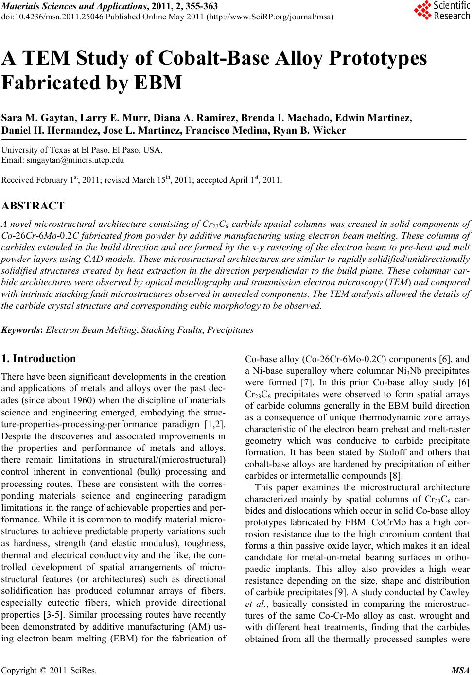 Materials Sciences and Applications, 2011, 2, 355-363 doi:10.4236/msa.2011.25046 Published Online May 2011 (http://www.SciRP.org/journal/msa) Copyright © 2011 SciRes. MSA 355 A TEM Study of Cobalt-Base Alloy Prototypes Fabricated by EBM Sara M. Gaytan, Larry E. Murr, Diana A. Ramirez, Brenda I. Machado, Edwin Martinez, Daniel H. Hernandez, Jose L. Martinez, Francisco Medina, Ryan B. Wicker University of Texas at El Paso, El Paso, USA. Email: smgaytan@miners.utep.edu Received February 1st, 2011; revised March 15th, 2011; accepted April 1st, 2011. ABSTRACT A novel microstructural architecture consisting of Cr23C6 carbide spatial columns was created in solid components of Co-26Cr-6Mo-0.2C fabricated from powder b y additive manufacturing using electron beam melting. These columns of carbides extended in the build direction and are formed by the x-y rastering of the electron beam to pre-heat and melt powder layers using CAD models. Th ese microstructural architectures are similar to rapidly so lidified/unidirectionally solidified structures created by heat extraction in the direction perpendicular to the build plane. These columnar car- bide architectures were observed by optical metallography and transmission electron microscopy (TEM) and compared with intrinsic stacking fau lt microstruc tures observed in annealed components. The TEM analysis allowed the details of the carbide crystal structure and corresponding cubic morphology to be observed. Keywords: Electron Beam Melting, Stacking Faults, Precipitates 1. Introduction There have been significant developments in the creation and applications of metals and alloys over the past dec- ades (since about 1960) when the discipline of materials science and engineering emerged, embodying the struc- ture-properties-processing-performance paradigm [1,2]. Despite the discoveries and associated improvements in the properties and performance of metals and alloys, there remain limitations in structural/(microstructural) control inherent in conventional (bulk) processing and processing routes. These are consistent with the corres- ponding materials science and engineering paradigm limitations in the range of achievable properties and per- formance. While it is common to modify material micro- structures to achieve predictable property variations such as hardness, strength (and elastic modulus), toughness, thermal and electrical conductivity and the like, the con- trolled development of spatial arrangements of micro- structural features (or architectures) such as directional solidification has produced columnar arrays of fibers, especially eutectic fibers, which provide directional properties [3-5]. Similar processing routes have recently been demonstrated by additive manufacturing (AM) us- ing electron beam melting (EBM) for the fabrication of Co-base alloy (Co-26Cr-6Mo-0.2C) components [6], and a Ni-base superalloy where columnar Ni3Nb precipitates were formed [7]. In this prior Co-base alloy study [6] Cr23C6 precipitates were observed to form spatial arrays of carbide columns generally in the EBM build direction as a consequence of unique thermodynamic zone arrays characteristic of the electron beam preheat and melt-raster geometry which was conducive to carbide precipitate formation. It has been stated by Stoloff and others that cobalt-base alloys are hardened by precipitation of either carbides or intermetallic compounds [8]. This paper examines the microstructural architecture characterized mainly by spatial columns of Cr23C6 car- bides and dislocations which occur in solid Co-base alloy prototypes fabricated by EBM. CoCrMo has a high cor- rosion resistance due to the high chromium content that forms a thin passive oxide layer, which makes it an ideal candidate for metal-on-metal bearing surfaces in ortho- paedic implants. This alloy also provides a high wear resistance depending on the size, shape and distribution of carbide precipitates [9]. A study conducted by Cawley et al., basically consisted in comparing the microstruc- tures of the same Co-Cr-Mo alloy as cast, wrought and with different heat treatments, finding that the carbides obtained from all the thermally processed samples were 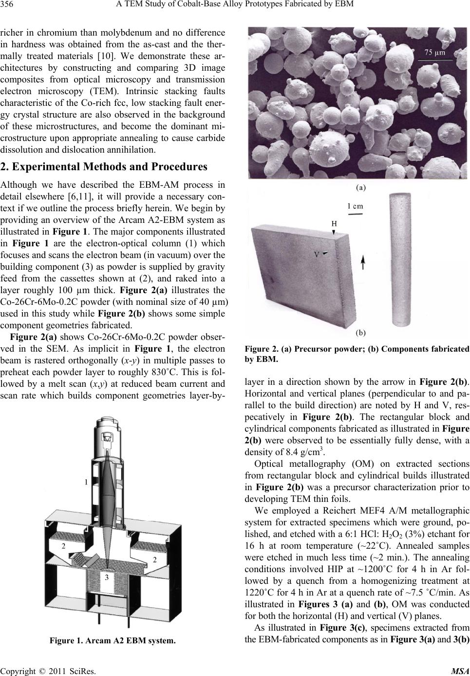 A TEM Study of Cobalt-Base Alloy Prototypes Fabricated by EBM Copyright © 2011 SciRes. MSA 356 richer in chromium than molybdenum and no difference in hardness was obtained from the as-cast and the ther- mally treated materials [10]. We demonstrate these ar- chitectures by constructing and comparing 3D image composites from optical microscopy and transmission electron microscopy (TEM). Intrinsic stacking faults characteristic of the Co-rich fcc, low stacking fault ener- gy crystal structure are also observed in the background of these microstructures, and become the dominant mi- crostructure upon appropriate annealing to cause carbide dissolution and dislocation annihilation. 2. Experimental Methods and Procedures Although we have described the EBM-AM process in detail elsewhere [6,11], it will provide a necessary con- text if we outline the process briefly herein. We begin by providing an overview of the Arcam A2-EBM system as illustrated in Figure 1. The major components illustrated in Figure 1 are the electron-optical column (1) which focuses and scans the electron beam (in vacuum) over the building component (3) as powder is supplied by gravity feed from the cassettes shown at (2), and raked into a layer roughly 100 µm thick. Figure 2(a) illustrates the Co-26Cr-6Mo-0.2C powder (with nominal size of 40 µm) used in this study while Figure 2(b) shows some simple component geometries fabricated. Figure 2(a) shows Co-26Cr-6Mo-0.2C powder obser- ved in the SEM. As implicit in Figure 1, the electron beam is rastered orthogonally (x-y) in multiple passes to preheat each powder layer to roughly 830˚C. This is fol- lowed by a melt scan (x,y) at reduced beam current and scan rate which builds component geometries layer-by- Figure 1. Arcam A2 EBM system. Figure 2. (a) Precursor powder; (b) Components fabricated by EBM. layer in a direction shown by the arrow in Figure 2(b). Horizontal and vertical planes (perpendicular to and pa- rallel to the build direction) are noted by H and V, res- pecatively in Figure 2(b). The rectangular block and cylindrical components fabricated as illustrated in Figure 2(b) were observed to be essentially fully dense, with a density of 8.4 g/cm3. Optical metallography (OM) on extracted sections from rectangular block and cylindrical builds illustrated in Figure 2(b) was a precursor characterization prior to developing TEM thin foils. We employed a Reichert MEF4 A/M metallographic system for extracted specimens which were ground, po- lished, and etched with a 6:1 HCl: H2O2 (3%) etchant for 16 h at room temperature (~22˚C). Annealed samples were etched in much less time (~2 min.). The annealing conditions involved HIP at ~1200˚C for 4 h in Ar fol- lowed by a quench from a homogenizing treatment at 1220˚C for 4 h in Ar at a quench rate of ~7.5 ˚C/min. As illustrated in Figures 3 (a) and (b), OM was conducted for both the horizontal (H) and vertical (V) planes. As illustrated in Figure 3(c), specimens extracted from the EBM-fabricated components as in Figure 3(a) and 3(b) 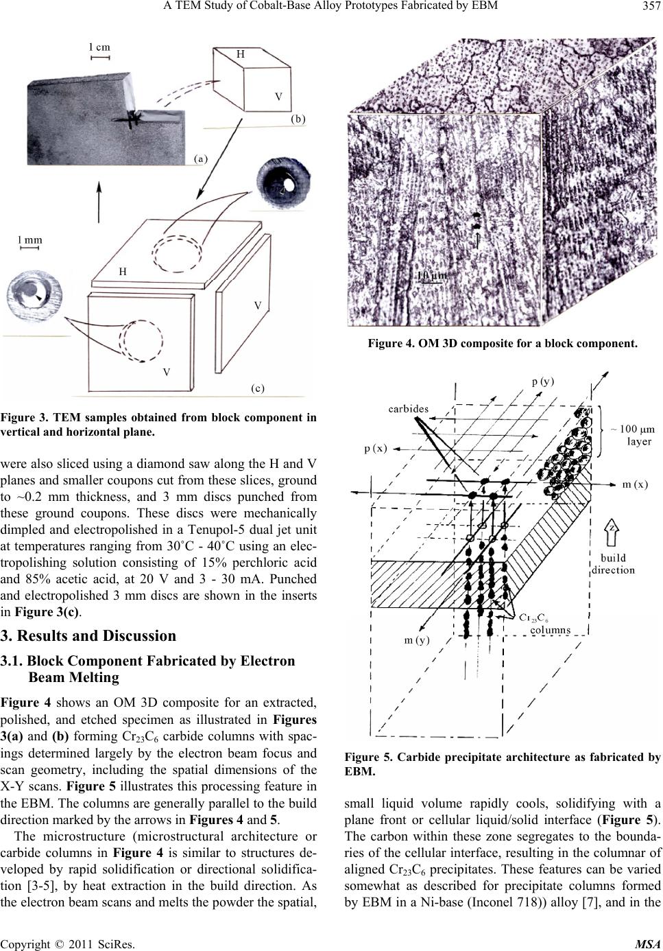 A TEM Study of Cobalt-Base Alloy Prototypes Fabricated by EBM Copyright © 2011 SciRes. MSA 357 Figure 3. TEM samples obtained from block component in vertical and horizontal plane. were also sliced using a diamond saw along the H and V planes and smaller coupons cut from these slices, ground to ~0.2 mm thickness, and 3 mm discs punched from these ground coupons. These discs were mechanically dimpled and electropolished in a Tenupol-5 dual jet unit at temperatures ranging from 30˚C - 40˚C using an elec- tropolishing solution consisting of 15% perchloric acid and 85% acetic acid, at 20 V and 3 - 30 mA. Punched and electropolished 3 mm discs are shown in the inserts in Figure 3(c). 3. Results and Discussion 3.1. Block Component Fabricated by Electron Beam Melting Figure 4 shows an OM 3D composite for an extracted, polished, and etched specimen as illustrated in Figures 3(a) and (b) forming Cr23C6 carbide columns with spac- ings determined largely by the electron beam focus and scan geometry, including the spatial dimensions of the X-Y scans. Figure 5 illustrates this processing feature in the EBM. The columns are generally parallel to the build direction marked by the arrows in Figures 4 and 5. The microstructure (microstructural architecture or carbide columns in Figure 4 is similar to structures de- veloped by rapid solidification or directional solidifica- tion [3-5], by heat extraction in the build direction. As the electron beam scans and melts the powder the spatial, Figure 4. OM 3D composite for a block component. Figure 5. Carbide precipitate architecture as fabricated by EBM. small liquid volume rapidly cools, solidifying with a plane front or cellular liquid/solid interface (Figure 5). The carbon within these zone segregates to the bounda- ries of the cellular interface, resulting in the columnar of aligned Cr23C6 precipitates. These features can be varied somewhat as described for precipitate columns formed by EBM in a Ni-base (Inconel 718)) alloy [7], and in the 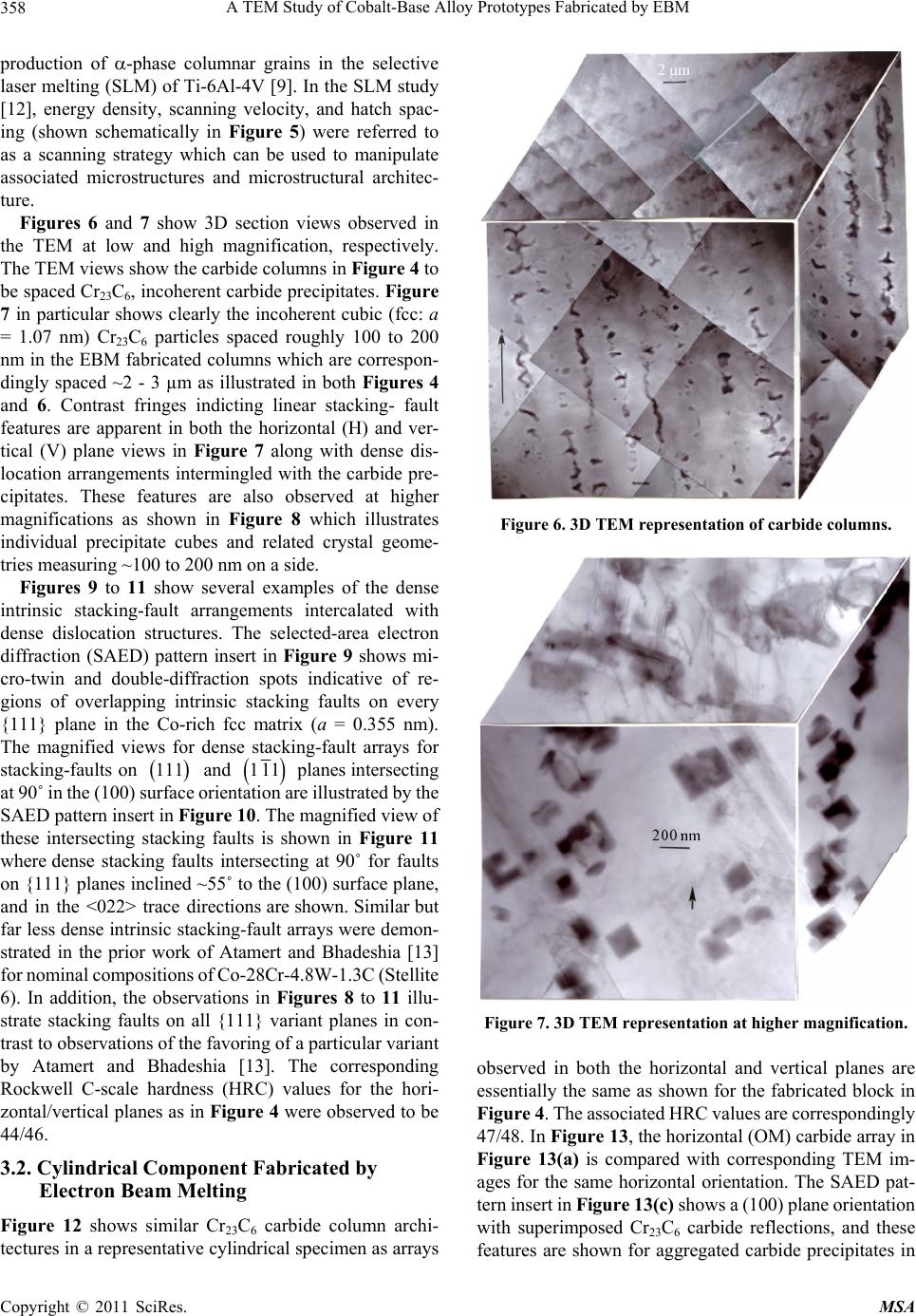 A TEM Study of Cobalt-Base Alloy Prototypes Fabricated by EBM Copyright © 2011 SciRes. MSA 358 production of -phase columnar grains in the selective laser melting (SLM) of Ti-6Al-4V [9]. In the SLM study [12], energy density, scanning velocity, and hatch spac- ing (shown schematically in Figure 5) were referred to as a scanning strategy which can be used to manipulate associated microstructures and microstructural architec- ture. Figures 6 and 7 show 3D section views observed in the TEM at low and high magnification, respectively. The TEM views show the carbide columns in Figure 4 to be spaced Cr23C6, incoherent carbide precipitates. Figure 7 in particular shows clearly the incoherent cubic (fcc: a = 1.07 nm) Cr23C6 particles spaced roughly 100 to 200 nm in the EBM fabricated columns which are correspon- dingly spaced ~2 - 3 µm as illustrated in both Figures 4 and 6. Contrast fringes indicting linear stacking- fault features are apparent in both the horizontal (H) and ver- tical (V) plane views in Figure 7 along with dense dis- location arrangements intermingled with the carbide pre- cipitates. These features are also observed at higher magnifications as shown in Figure 8 which illustrates individual precipitate cubes and related crystal geome- tries measuring ~100 to 200 nm on a side. Figures 9 to 11 show several examples of the dense intrinsic stacking-fault arrangements intercalated with dense dislocation structures. The selected-area electron diffraction (SAED) pattern insert in Figure 9 shows mi- cro-twin and double-diffraction spots indicative of re- gions of overlapping intrinsic stacking faults on every {111} plane in the Co-rich fcc matrix (a = 0.355 nm). The magnified views for dense stacking-fault arrays for stacking-faults on 111 and 111 planes intersecting at 90˚ in the (100) surface orientation are illustrated by the SAED pattern insert in Figure 10. The magnified view of these intersecting stacking faults is shown in Figure 11 where dense stacking faults intersecting at 90˚ for faults on {111} planes inclined ~55˚ to the (100) surface plane, and in the <022> trace directions are shown. Similar but far less dense intrinsic stacking-fault arrays were demon- strated in the prior work of Atamert and Bhadeshia [13] for nominal compositions of Co-28Cr-4.8W-1.3C (Stellite 6). In addition, the observations in Figures 8 to 11 illu- strate stacking faults on all {111} variant planes in con- trast to observations of the favoring of a particular variant by Atamert and Bhadeshia [13]. The corresponding Rockwell C-scale hardness (HRC) values for the hori- zontal/vertical planes as in Figure 4 were observed to be 44/46. 3.2. Cylindrical Component Fabricated by Electron Beam Melting Figure 12 shows similar Cr23C6 carbide column archi- tectures in a representative cylindrical specimen as arrays Figure 6. 3D TEM representation of carbide columns. Figure 7. 3D TEM representation at higher magnification. observed in both the horizontal and vertical planes are essentially the same as shown for the fabricated block in Figure 4. The associated HRC values are correspondingly 47/48. In Figure 13, the horizontal (OM) carbide array in Figure 13(a) is compared with corresponding TEM im- ages for the same horizontal orientation. The SAED pat- tern insert in Figure 13 (c) shows a (100) plane orientation with superimposed Cr23C6 carbide reflections, and these features are shown for aggregated carbide precipitates in  A TEM Study of Cobalt-Base Alloy Prototypes Fabricated by EBM Copyright © 2011 SciRes. MSA 359 (a) (b) (c) (d) Figure 8. Cr23C6 precipitates. Figure 9. Stacking faults and double-diffraction spots. Figure 14 which range in particle size from ~50 to 500 nm, with their (100)-fcc diffraction pattern superimposed on the Co-rich matrix SAED pattern insert in Figure 14. Figure 10. Intersecting intrinsic staking faults. Figure 11. Magnified image of stacking faults. Figure 14 also shows a high density of dislocations es- pecially associated with the carbide precipitates, the SAED pattern insert shows [100] Cr23C6 zone axis supe- rimposed on [112] fcc Co-rich matrix zone axis. Figure 15 shows dense stacking-fault arrays similar to those shown in Figures 9-11 for a block specimen (Figure 3). Here again, the intersections of faults on {111} planes which intersect at 90˚ produce diffraction contrast features for these intersecting {111} planes at 45˚. The SAED pat- tern insert in Figure 15 also shows the same (100) orien- tation as observed in Figures 9-11, along with some extra reflections characteristic of twin faults created by the systematic, overlapping intrinsic stacking faults. As shown previously by Gaytan, et al. [6], the fracture surface for failed cylindrical samples illustrated a spatial  A TEM Study of Cobalt-Base Alloy Prototypes Fabricated by EBM Copyright © 2011 SciRes. MSA 360 Figure 12. Columnar architecture in cylindrical component. Figure 13. OM and TEM images of carbides. Figure 14. Cr23C6 particles interacting with or generating dislocations. Figure 15. Dense, intersecting stacking faults. array of ductile dimples matching the cubic-shape carbide precipitate array illustrated typically in Figures 12 and 13 in the horizontal plane, coincident with the fracture sur- face; this feature is illustrated in Figure 16. Correspond- ing UTS and elongation were 1.45 GPa and 3.6%, re- spectively, as previously determined by Gaytan, et al. [6].  A TEM Study of Cobalt-Base Alloy Prototypes Fabricated by EBM Copyright © 2011 SciRes. MSA 361 (a) (b) Figure 16. Fractured surface from a cylindrical component fabricated by EBM, (a) Low magnification and (b) High magnification image. Grain boundaries and regular grain structures were difficult to differentiate in the carbide arrays but more regular Cr23C6 precipitation and corresponding etching made them somewhat apparent as noted in the etching patterns of Figure 4. Here the average grain sizes are observed to be about 20 µm, or an order of magnitude larger than the carbide column arrays. There seems to be a preference for [100] orientations parallel to the build direction, which is also characteristic of orientation pre- ference in commercial processed copper billets and plate. 3.3. Components Fabricated by Electron Beam Melting after Annealing In the annealed condition, the carbide column architectures disappear, leaving an, fcc grain structure containing a pro- pensity of annealing twin boundaries. While Cr23C6 car- bides generally dissolve in the grain matrix, there are resi- dual carbides in the grain boundaries, and these promote exaggerated etching, especially at high angle or high energy grain boundaries. In this regard, note that there is no car- bide-associated etching along the straight coherent twin boundaries where the energy is roughly the same as the stacking faults (~15 mJ/m2), and about 0.03 times the grain boundary free energy [14]. These features are illustrated typically in Figure 17 where the average grain size, in- cluding twinned grains (light grains) was ~35 µm. This is roughly a 75% increase over the as-fabricated Co-26Cr- 6Mo-0.2C components (Figure 2(b)). Correspondingly, the residual hardness (HRC) was 40 in contrast to ~47 for the as-fabricated components; a decrease of ~15%. The high density of stacking faults and twin-faults declined measurably as illustrated in comparative views of stacking faults shown in Figures 18-20, where Figure 18 represents a surface orientation of (112) with 110 direction shown by the arrow. Figure 19 is a magnified view of stacking faults in the (100) surface orientation with their traces in the <022> directions. Figure 20, like Figures 18 and 19, illu- strates intrinsic stacking faults on essentially all {111} plane variants in contrast to the prior Co-base alloy TEM observations by Atamert and Bhadeshia [13]. It is of interest to compare, retrospectively, the annealed, equiaxed grain structure (Figure 17) and the associated stacking fault microstructure (Figures 18-20) with the more dense stacking fault microstructure and unique car- bide microstructural architectures created by EBM fabri- cation as illustrated in Figures 9-11 and 15, and Figures 4, 6-8, and 12-14. Figure 18 shows a TEM bright-field im- age of intrinsic stacking faults in the (112) orientation for the annealed Co-base alloy in Figure 17. The arrow in- dicates the trace of the 110 direction, while Figure 19 is a TEM image of stacking faults intersecting at ~90˚ in a (100) grain orientation and Figure 20 shows multi- variant {111} stacking faults in the annealed Co-base alloy. These comparisons provide a compelling example of a controlled microstructural architecture in contrast to the conventional (carbide) microstructural reime. Alth- ough the Cr23C6 column architectures are not continuous or even proximate carbide particles, the concept as it can be created through systematic, additive manufacturing using EBM, suggests a revolutionary extension of the conventional microstructure-property-processing-perfor- mance materials science an engineering paradigm. Indeed, in the same way compositions (in this case especially carbon content) or chemistries of alloy systems can in- fluence the microstructure-property relationships in par- ticular, the prospects for microstructural architecture ma- nipulation and the attendant property-processing-perfor- mance variations, attest to the novelty and potential fea- tures of the concept. Increasing the carbon content in the Co-26Cr-6Mo-C alloy, especially to more contemporary levels for aerospace superalloy applications (> 0.5C) should have a controlling effect on the carbide particle  A TEM Study of Cobalt-Base Alloy Prototypes Fabricated by EBM Copyright © 2011 SciRes. MSA 362 Figure 17. EBM fabricated components after annealing treatment. Figure 18. Intrinsic stacking faults in the (112) orientation. densities (or spacings) in the EBM-produced columns (Figures 4, 6 and 7). This in turn should influence simple mechanical properties such as residual hardness (even directionally), strength, elongation, and even the elastic Figure 19. Stacking faults intersecting at ~90˚ in a (100) grain orientation. Figure 20. Multivariant {111} stacking faults in the an- nealed Co-base alloy. (Young’s) modulus. The latter would be especially nota- ble if the carbide particle columns began to act somewhat like fiber-arrays in a matrix where the volumetric addition  A TEM Study of Cobalt-Base Alloy Prototypes Fabricated by EBM Copyright © 2011 SciRes. MSA 363 of such reinforcing features alter the elastic modulus in relation to their spatial relationship as it influences the so-called rule of mixtures for the ideal isostrain condition where the stress is applied in the direction of the fibers. Of course these features are only speculative at this point. 4. Conclusions Using TEM, we have illustrated the details of Cr23C6 carbide columns created by the systematic, spatial scans of an electron beam in the additive manufacturing of Co-26Cr-6Mo-0.2C prototypes using EBM. These col- umns represent an example of a controlled microstructural architecture. In this study, we have in principle compared these uniquely fabricated architectures with more con- ventional, stacking fault microstructures by annealing the carbides and their attendant architectures. These archi- tectures represent length scales ranging from microns-to- nanometers which may be extended systematically to the macroscale represented by millimeters-to-meters. The TEM analyses have demonstrated Cr23C6 carbides to be exclusive in the formation of column architectures with spacings of 1 - 3 µm for carbide particles ranging nomi- nally from <100 nm to >200 nm. 5. Acknowledgements This work was supported in part by Mr. & Mrs. MacIn- tosh Murchison endowments at The University of Texas at El Paso. REFERENCES [1] R. Roy, “Materials Science and Engineering in the United States,” The Pennsylvania State University Press, State College, 1970. [2] Materials Science and Engineering for the 1990s, “Main- taining Competitiveness in the Age of Materials,” Na- tional Academy Press, Washington, 1989. [3] G. A. Chadwick, “Eutectic Solidification,” In: T. J. Hughel, Ed., Liquids: Structure, Properties, Solid Interactions, Elsevier, New York, 1965, pp. 238-255. [4] H. W. Weart and J. D. Mack, “Eutectic Solidification Structures,” Transactions of the Metallurgical Society of AIME, Vol. 212, 1958, pp. 664-671. [5] R. W. Kraft, “Eutectic Solidification,” Journal of Metals, Vol. 8, No. 2, 1966, pp. 192-198. [6] S. M. Gaytan, L. E. Murr, E. Martinez, J. L. Martinez, B. I. Machado, D. A. Ramirez, F. Medina, S. Collins and R. B. Wicker, “Comparisons of Microstructures and Me- chanical Properties for Solid and Mesh Cobalt-Base Alloy Prototypes Fabricated by Electron Beam Melting,” Me- tallurgical and Materials Transactions A, Vol. 41, No. 12, 2010, pp. 3216-3227. doi:10.1007/s11661-010-0388-y [7] A. Strondl, R. Fischer, G. Frommeyer and A.Schneider, “Investigations of MX and γ’/γ’’ precipitates in the Nick- el-based Superalloy 718 Produced by Electron Beam Melting,” Materials Science and Engineering A, Vol. 480, No. 1-2, 2008, pp. 138-147. doi:10.1016/j.msea.2007.07.012 [8] C. T. Sims, N. S. Stoloff and W. C. Hagel, “Superalloys II,” John Wiley & Sons, New York, 1987. [9] G. D. Janaki, “Microstructure and Wear Properties of LENS® Deposited Medical Grade CoCrMo,” Journal of Materials Science: Materials in Medicine, Vol. 19, No. 5, 2008, pp. 2105-2111. doi:10.1007/s10856-007-3078-6 [10] J. Cawley, J. E. P. Metcalf, A. H. Jones, T. J. Band and D. S. Skupien, “A Tribological Study of Cobalt Chromium Molybdenum Alloys Used in Metal-on-Metal Resurfacing Hip Arthroplasty,” Wear, Vol. 255, No. 7-12, 2003, pp. 999-1006. doi:10.1016/S0043-1648(03)00046-2 [11] L. E. Murr, E. V. Esquivel, S. A. Quinones, S. M. Gaytan, M. I. Lopez, E. Y. Martinez, F. Medina, D. H. Hernandez, E. Martinez, J. L. Martinez, S. W. Stafford, D. K. Brown, T. Hoppe, W. Meyers, U. Lindhe and R. B. Wicker, “Mi- crostructures and Mechanical Properties of Electron Beam-Rapid Manufactured Ti-6Al-4V Biomedical Pro- totypes Compared to Wrought Ti-6Al-4V,” Materials Characterization, Vol. 60, No. 2, 2009, pp. 96-105. doi:10.1016/j.matchar.2008.07.006 [12] L. Thijs, F. Verhaeghe, T. Craeghs, J. van Humbeeck and J.-P. Kruth, “A Study of the Microstructural Evolution during Selective Laser Melting of Ti-6Al-4V,” Acta Ma- terialia, Vol. 58, No. 9, 2010, pp. 3303-3312. doi:10.1016/j.actamat.2010.02.004 [13] S. Atamert and H. K. D. H. Bhadeshia, “Comparison of the Microstructures and Abrasive Wear Properties of Stellite Hardfacing Alloys Deposited by Arc Welding and Laser Cladding,” Metallurgical and Materials Transac- tions, Vol. 20, No. 6, 1989, pp. 1037-1054. doi:10.1007/BF02650140 [14] L. E. Murr, “Interfacial Phenomena in Metals, and Al- loys,” Addison-Wesley, Reading, 1975. |