Paper Menu >>
Journal Menu >>
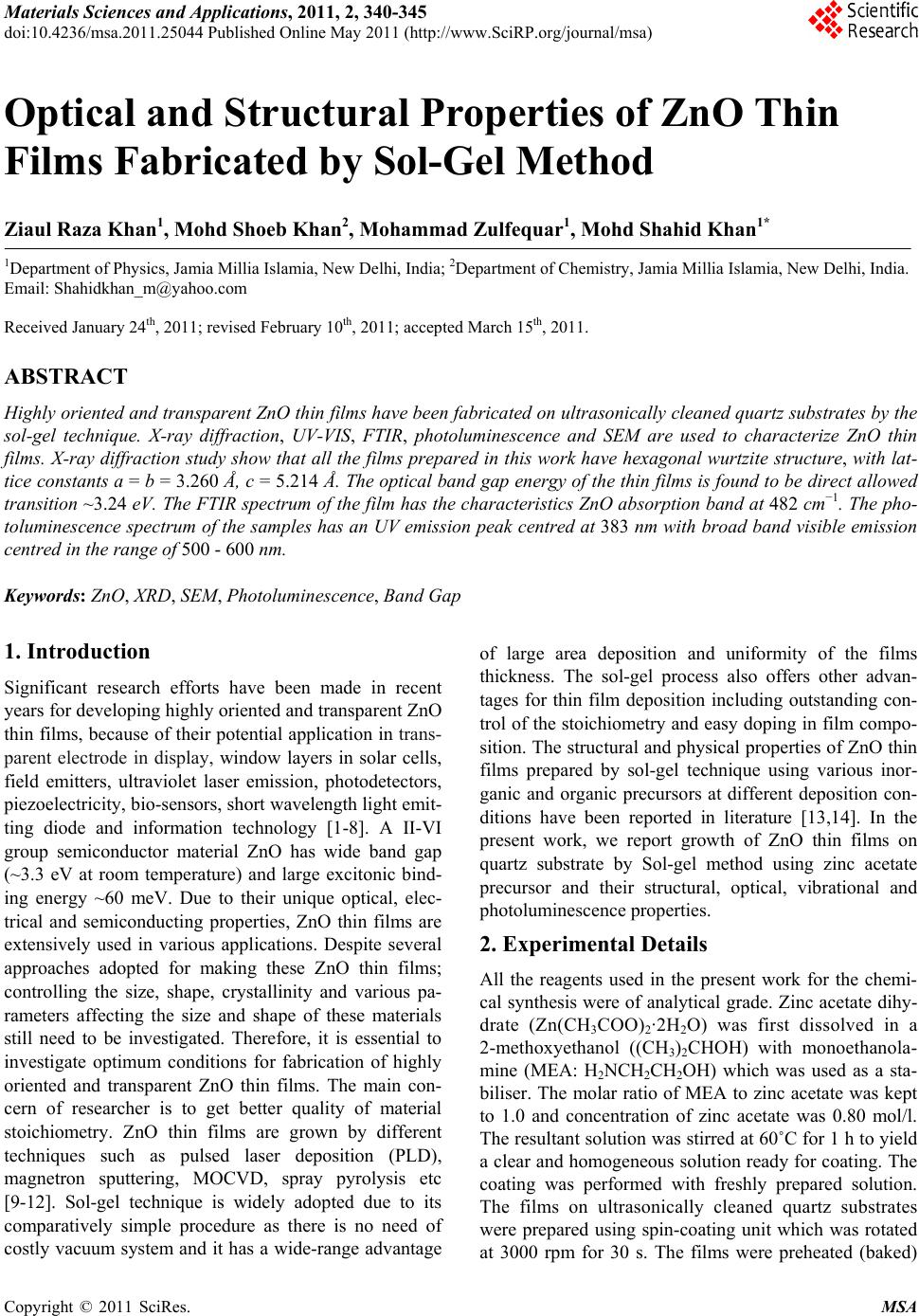 Materials Sciences and Applications, 2011, 2, 340-345 doi:10.4236/msa.2011.25044 Published Online May 2011 (http://www.SciRP.org/journal/msa) Copyright © 2011 SciRes. MSA Optical and Structural Properties of ZnO Thin Films Fabricated by Sol-Gel Method Ziaul Raza Khan1, Mohd Shoeb Khan2, Mohammad Zulfequar1, Mohd Shahid Khan1* 1Department of Physics, Jamia Millia Islamia, New Delhi, India; 2Department of Chemistry, Jamia Millia Islamia, New Delhi, India. Email: Shahidkhan_m@yahoo.com Received January 24th, 2011; revised February 10th, 2011; accepted March 15th, 2011. ABSTRACT Highly oriented and transparent ZnO thin films have been fabricated on ultrasonically cleaned quartz substrates by the sol-gel technique. X-ray diffraction, UV-VIS, FTIR, photoluminescence and SEM are used to characterize ZnO thin films. X-ray diffraction study show that all the films prepared in this work have hexagonal wurtzite structure, with lat- tice constants a = b = 3.260 Å, c = 5.214 Å. The optical band gap energy of the thin films is found to be direct allowed transition ~3.24 eV. The FTIR spectrum of the film has the characteristics ZnO absorption band at 482 cm−1. The pho- toluminescence spectrum of the samples has an UV emission peak centred at 383 nm with broad band visible emission centred in the range of 500 - 600 nm. Keywords: ZnO, XRD, SEM, Photoluminescence, Band Gap 1. Introduction Significant research efforts have been made in recent years for developing highly oriented and transparent ZnO thin films, because of their potential application in trans- parent electrode in display, window layers in solar cells, field emitters, ultraviolet laser emission, photodetectors, piezoelectricity, bio-sensors, short wavelength light emit- ting diode and information technology [1-8]. A II-VI group semiconductor material ZnO has wide band gap (~3.3 eV at room temperature) and large excitonic bind- ing energy ~60 meV. Due to their unique optical, elec- trical and semiconducting properties, ZnO thin films are extensively used in various applications. Despite several approaches adopted for making these ZnO thin films; controlling the size, shape, crystallinity and various pa- rameters affecting the size and shape of these materials still need to be investigated. Therefore, it is essential to investigate optimum conditions for fabrication of highly oriented and transparent ZnO thin films. The main con- cern of researcher is to get better quality of material stoichiometry. ZnO thin films are grown by different techniques such as pulsed laser deposition (PLD), magnetron sputtering, MOCVD, spray pyrolysis etc [9-12]. Sol-gel technique is widely adopted due to its comparatively simple procedure as there is no need of costly vacuum system and it has a wide-range advantage of large area deposition and uniformity of the films thickness. The sol-gel process also offers other advan- tages for thin film deposition including outstanding con- trol of the stoichiometry and easy doping in film compo- sition. The structural and physical properties of ZnO thin films prepared by sol-gel technique using various inor- ganic and organic precursors at different deposition con- ditions have been reported in literature [13,14]. In the present work, we report growth of ZnO thin films on quartz substrate by Sol-gel method using zinc acetate precursor and their structural, optical, vibrational and photoluminescence properties. 2. Experimental Details All the reagents used in the present work for the chemi- cal synthesis were of analytical grade. Zinc acetate dihy- drate (Zn(CH3COO)2·2H2O) was first dissolved in a 2-methoxyethanol ((CH3)2CHOH) with monoethanola- mine (MEA: H2NCH2CH2OH) which was used as a sta- biliser. The molar ratio of MEA to zinc acetate was kept to 1.0 and concentration of zinc acetate was 0.80 mol/l. The resultant solution was stirred at 60˚C for 1 h to yield a clear and homogeneous solution ready for coating. The coating was performed with freshly prepared solution. The films on ultrasonically cleaned quartz substrates were prepared using spin-coating unit which was rotated at 3000 rpm for 30 s. The films were preheated (baked) 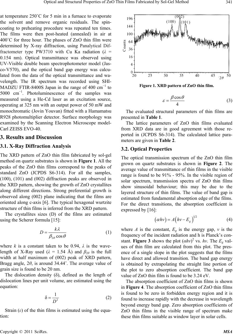 Optical and Structural Properties of ZnO Thin Films Fabricated by Sol-Gel Method Copyright © 2011 SciRes. MSA 341 at temperature 250˚C for 5 min in a furnace to evaporate the solvent and remove organic residuals. The spin- coating to preheating procedure was repeated ten times. The films were then post-heated (annealed) in air at 400˚C for three hour. The phases of ZnO thin film were determined by X-ray diffraction, using Panalytical Dif- fractometer type PW3710 with Cu Ka radiation (λ = 0.154 nm). Optical transmittance was observed using UV-Visible double beam spectrophotometer model (Jas- co-V570), and the optical band gap energy was calcu- lated from the data of the optical transmittance and wa- velength. The IR spectrum was recorded using SHI- MADZU FTIR-8400S Japan in the range of 400 cm−1 to 5000 cm−1. Photoluminescence of the samples was measured using a He-Cd laser as an excitation source, operating at 325 nm with an output power of 50 mW and monochromatic (Jovin Youvan) fitted with a Hamamatsu R928 photomultiplier detector. Surface morphology was examined by the Scanning Electron Microscope model- Carl ZEISS EVO-40. 3. Results and Discussion 3.1. X-Ray Diffraction Analysis The XRD pattern of ZnO thin film fabricated by sol-gel method on quartz substrates is shown in Figure 1. All the peaks of the ZnO thin films correspond to the peaks of standard ZnO (JCPDS S6-314). For all the samples, (100), (101) and (002) diffraction peaks are observed in the XRD pattern, showing the growth of ZnO crystallites along different directions. Strong preferential growth is observed along (002) plane indicating that the films are oriented along c-axis [6]. The typical hexagonal wurtzite structure of thin films is inferred from the XRD pattern. The crystallites sizes (D) of the films are estimated using the Scherer formula [15]: 2cos k D (1) where k is a constant taken to be 0.94, λ is the wave- length of X-Ray used (λ = 1.54 Å) and β2θ is the full width at half maximum of (002) peak of XRD pattern, Bragg angle, 2θ, is around 34.44˚. The average value of grain size is found to be 20 nm. The dislocation density (δ), defined as the length of dislocation lines per unit volume, are estimated using the equation: 2 1 δD (2) Strain (ε) of the thin films is estimated using the equa- tion: Figure 1. XRD pattern of ZnO thin film. cos 4 (3) The evaluated structural parameters of thin films are presented in Table 1. The lattice parameters of ZnO thin films evaluated from XRD data are in good agreement with those re- ported in (JCPDS S6-314). The calculated lattice para- meters are given in Table 2. 3.2. Optical Properties The optical transmission spectrum of the ZnO thin film grown on quartz substrates is shown in Figure 2. The average value of transmittance of thin films in the visible range is found to be 91% - 95%. In the visible region of solar spectrum, transmission spectra of ZnO thin films show sinusoidal behaviour; this may be due to the layered structure of thin films. The value of band gap is estimated from fundamental absorption edge of the films. For the direct transitions, the absorption coefficient is expressed by [16]: 12 g hvA hvE (4) where A is the constant, Eg is the energy gap, ν is the frequency of the incident radiation and h is Planck’s con- stant. Figure 3 shows the plot (αhν)2 vs. hν. The Eg val- ues of thin film are calculated from this plot. The pres- ence of a single slope in the plot suggests that the films have direct and allowed transition. The band gap energy is obtained by extrapolating the straight line portion of the plot to zero absorption coefficient. The band gap value of ZnO thin film is found to be 3.24 eV. The absorption coefficient of ZnO thin films is shown in Figure 4. The absorption coefficient of ZnO thin films is found to be zero in forbidden energy region and it is found to increase rapidly with the decrease in wavelength beyond energy band gap. Zero absorption coefficients of ZnO thin films in the visible range of spectrum make these thin films suitable as window layer in solar cells. 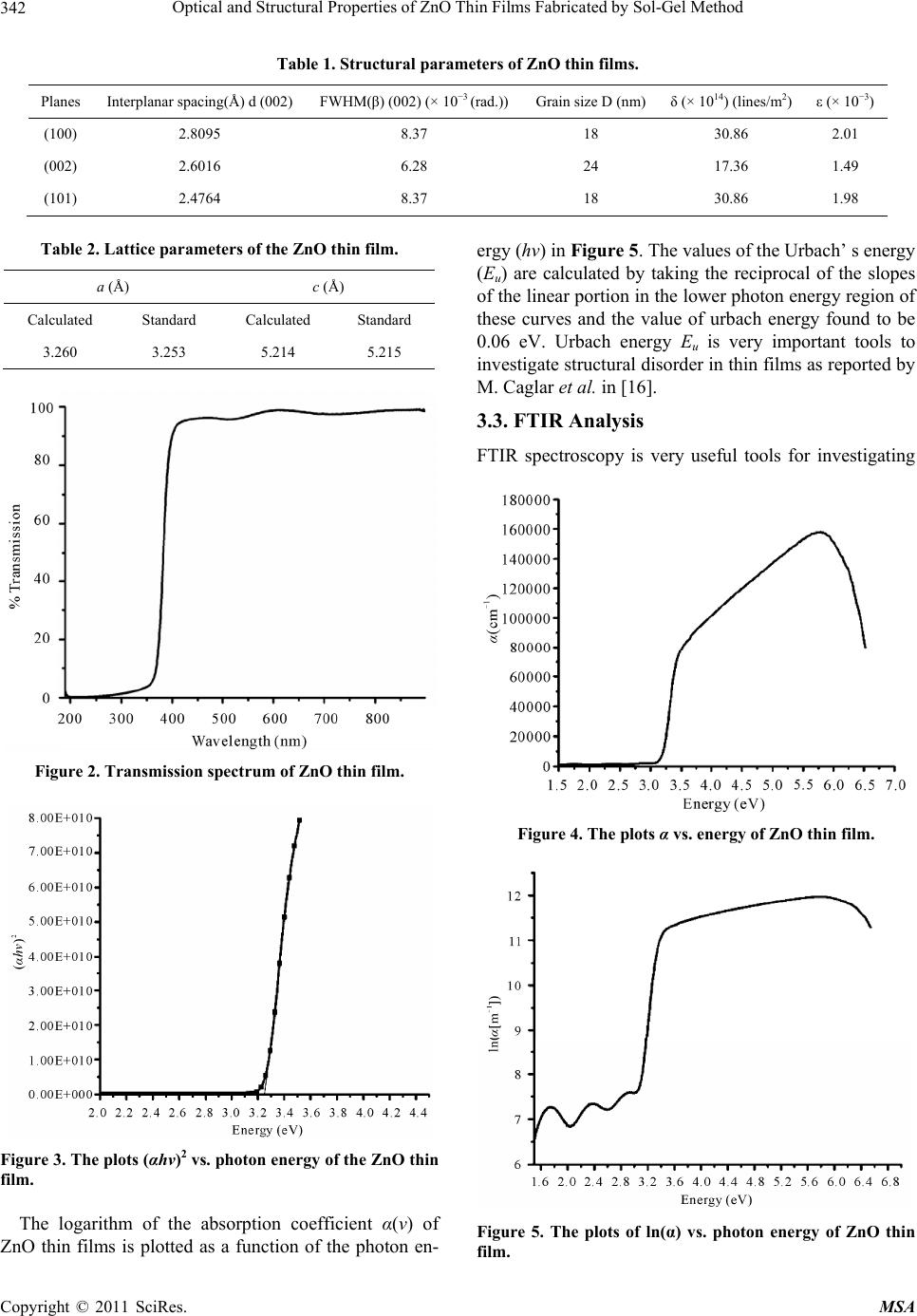 Optical and Structural Properties of ZnO Thin Films Fabricated by Sol-Gel Method Copyright © 2011 SciRes. MSA 342 Table 1. Structural parameters of ZnO thin films. Planes Interplanar spacing(Å) d (002) FWHM(β) (002) (× 10−3 (rad.))Grain size D (nm)δ (× 1014) (lines/m2) ε (× 10−3) (100) 2.8095 8.37 18 30.86 2.01 (002) 2.6016 6.28 24 17.36 1.49 (101) 2.4764 8.37 18 30.86 1.98 Table 2. Lattice parameters of the ZnO thin film. a (Å) c (Å) Calculated Standard Calculated Standard 3.260 3.253 5.214 5.215 Figure 2. Transmission spectrum of ZnO thin film. Figure 3. The plots (αhν)2 vs. photon energy of the ZnO thin film. The logarithm of the absorption coefficient α(ν) of ZnO thin films is plotted as a function of the photon en- ergy (hν) in Figure 5. The values of the Urbach’ s energy (Eu) are calculated by taking the reciprocal of the slopes of the linear portion in the lower photon energy region of these curves and the value of urbach energy found to be 0.06 eV. Urbach energy Eu is very important tools to investigate structural disorder in thin films as reported by M. Caglar et al. in [16]. 3.3. FTIR Analysis FTIR spectroscopy is very useful tools for investigating Figure 4. The plots α vs. energy of ZnO thin film. Figure 5. The plots of ln(α) vs. photon energy of ZnO thin film. 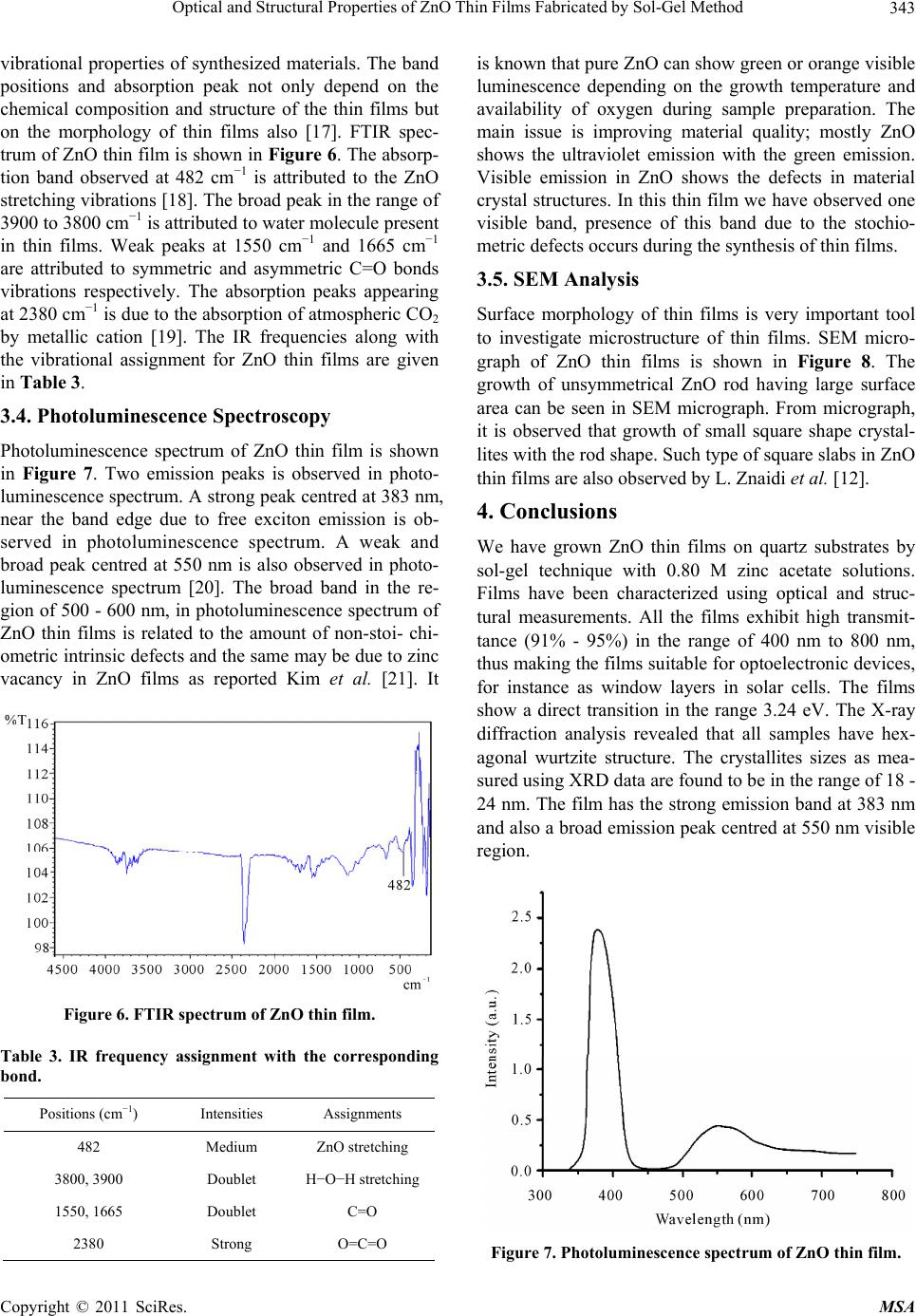 Optical and Structural Properties of ZnO Thin Films Fabricated by Sol-Gel Method Copyright © 2011 SciRes. MSA 343 vibrational properties of synthesized materials. The band positions and absorption peak not only depend on the chemical composition and structure of the thin films but on the morphology of thin films also [17]. FTIR spec- trum of ZnO thin film is shown in Figure 6. The absorp- tion band observed at 482 cm−1 is attributed to the ZnO stretching vibrations [18]. The broad peak in the range of 3900 to 3800 cm−1 is attributed to water molecule present in thin films. Weak peaks at 1550 cm−1 and 1665 cm−1 are attributed to symmetric and asymmetric C=O bonds vibrations respectively. The absorption peaks appearing at 2380 cm−1 is due to the absorption of atmospheric CO2 by metallic cation [19]. The IR frequencies along with the vibrational assignment for ZnO thin films are given in Table 3. 3.4. Photoluminescence Spectroscopy Photoluminescence spectrum of ZnO thin film is shown in Figure 7. Two emission peaks is observed in photo- luminescence spectrum. A strong peak centred at 383 nm, near the band edge due to free exciton emission is ob- served in photoluminescence spectrum. A weak and broad peak centred at 550 nm is also observed in photo- luminescence spectrum [20]. The broad band in the re- gion of 500 - 600 nm, in photoluminescence spectrum of ZnO thin films is related to the amount of non-stoi- chi- ometric intrinsic defects and the same may be due to zinc vacancy in ZnO films as reported Kim et al. [21]. It Figure 6. FTIR spectrum of ZnO thin film. Table 3. IR frequency assignment with the corresponding bond. Positions (cm−1) Intensities Assignments 482 Medium ZnO stretching 3800, 3900 Doublet H−O−H stretching 1550, 1665 Doublet C=O 2380 Strong O=C=O is known that pure ZnO can show green or orange visible luminescence depending on the growth temperature and availability of oxygen during sample preparation. The main issue is improving material quality; mostly ZnO shows the ultraviolet emission with the green emission. Visible emission in ZnO shows the defects in material crystal structures. In this thin film we have observed one visible band, presence of this band due to the stochio- metric defects occurs during the synthesis of thin films. 3.5. SEM Analysis Surface morphology of thin films is very important tool to investigate microstructure of thin films. SEM micro- graph of ZnO thin films is shown in Figure 8. The growth of unsymmetrical ZnO rod having large surface area can be seen in SEM micrograph. From micrograph, it is observed that growth of small square shape crystal- lites with the rod shape. Such type of square slabs in ZnO thin films are also observed by L. Znaidi et al. [12]. 4. Conclusions We have grown ZnO thin films on quartz substrates by sol-gel technique with 0.80 M zinc acetate solutions. Films have been characterized using optical and struc- tural measurements. All the films exhibit high transmit- tance (91% - 95%) in the range of 400 nm to 800 nm, thus making the films suitable for optoelectronic devices, for instance as window layers in solar cells. The films show a direct transition in the range 3.24 eV. The X-ray diffraction analysis revealed that all samples have hex- agonal wurtzite structure. The crystallites sizes as mea- sured using XRD data are found to be in the range of 18 - 24 nm. The film has the strong emission band at 383 nm and also a broad emission peak centred at 550 nm visible region. Figure 7. Photoluminescence spectrum of ZnO thin film. 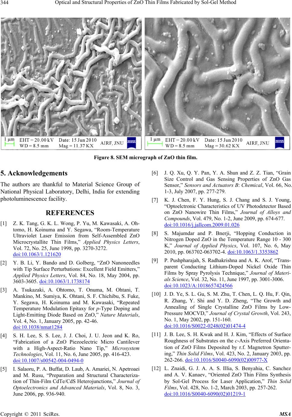 Optical and Structural Properties of ZnO Thin Films Fabricated by Sol-Gel Method Copyright © 2011 SciRes. MSA 344 Figure 8. SEM micrograph of ZnO thin film. 5. Acknowledgements The authors are thankful to Material Science Group of National Physical Laboratory, Delhi, India for extending photoluminescence facility. REFERENCES [1] Z. K. Tang, G. K. L. Wong, P. Yu, M. Kawasaki, A. Oh- tomo, H. Koinuma and Y. Segawa, “Room-Temperature Ultraviolet Laser Emission from Self-Assembled ZnO Microcrystallite Thin Films,” Applied Physics Letters, Vol. 72, No. 25, June 1998, pp. 3270-3272. doi:10.1063/1.121620 [2] Y. B. Li, Y. Bando and D. Golberg, “ZnO Nanoneedles with Tip Surface Perturbations: Excellent Field Emitters,” Applied Physics Letters, Vol. 84, No. 18, May 2004, pp. 3603-3605. doi:10.1063/1.1738174 [3] A. Tsukazaki, A. Ohtomo, T. Onuma, M. Ohtani, T. Mankino, M. Sumiya, K. Ohtani, S. F. Chichibu, S. Fuke, Y. Segawa, H. Koinuma and M. Kawasaki, “Repeated Temperature Modulation Epitaxy for p-Type Doping and Light-Emitting Diode Based on ZnO,” Nature Materials, Vol. 4, No. 1, January 2005, pp. 42-46. doi:10.1038/nmat1284 [4] S. H. Lee, S. S. Lee, J. J. Choi, J. U. Jeon and K. Ro, “Fabrication of a ZnO Piezoelectric Micro Cantilever with a High-Aspect-Ratio Nano Tip,” Microsystem Technologies, Vol. 11, No. 6, June 2005, pp. 416-423. doi:10.1007/s00542-004-0494-0 [5] I. Salaoru, P. A. Buffat, D. Laub, A. Amariei, N. Apetroaei and M. Rusu, “Preparation and Structural Characteriza- tion of Thin-Film CdTe/CdS Heterojunctions,” Journal of Optoelectronics and Advanced Materials, Vol. 8, No. 3, June 2006, pp. 936-940. [6] J. Q. Xu, Q. Y. Pan, Y. A. Shun and Z. Z. Tian, “Grain Size Control and Gas Sensing Properties of ZnO Gas Sensor,” Sensors and Actuators B: Chemical, Vol. 66, No. 1-3, July 2007, pp. 277-279. [7] K. J. Chen, F. Y. Hung, S. J. Chang and S. J. Young, “Optoelctronic Characteristics of UV Photodetector Based on ZnO Nanowire Thin Films,” Journal of Alloys and Compounds, Vol. 479, No. 1-2, June 2009, pp. 674-677. doi:10.1016/j.jallcom.2009.01.026 [8] S. Majumdar and P. Bnerji, “Hopping Conduction in Nitrogen Doped ZnO in the Temperature Range 10 - 300 K,” Journal of Applied Physics, Vol. 107, No. 6, May 2010, pp. 063702-063702-4. doi:10.1063/1.3353862 [9] P. Pushpharajah, S. Radhakrishna and A. K. Arof, “Trans- parent Conducting Lithium-Doped Nickel Oxide Thin Films by Spray Pyrolysis Technique,” Journal of Materi- als Science, Vol. 32, No. 11, June 1997, pp. 3001-3006. doi:10.1023/A:1018657424566 [10] J. D. Ye, S. L. Gu, S. M. Zhu, T. Chen, L. Q. Hu, F. Qin, R. Zhang, Y. Shi and Y. D. Zheng, “The Growth and Annealing of Single Crystalline ZnO Films by Low- Pressure MOCVD,” Journal of Crystal Growth, Vol. 243, No. 1, May 2002, pp. 151-160. doi:10.1016/S0022-0248(02)01474-4 [11] J. B. Lee, S. H. Kwak and H. J. Kim, “Effects of Surface Roughness of Substrates on the c-Axis Preferred Orienta- tion of ZnO Films Deposited by r.f. Magnetron Sputter- ing,” Thin Solid Films, Vol. 423, No. 2, January 2003, pp. 262-266. doi:10.1016/S0040-6090(02)00977-X [12] L. Znaidi, G. J. A. A. S. Illia, S. Benyahia, C. Sanchez and A. V. Kanaev, “Oriented ZnO Thin Films Synthesis by Sol-Gel Process for Laser Application,” Thin Solid Films, Vol. 428, No. 1-2, March 2003, pp. 257-262. doi:10.1016/S0040-6090(02)01219-1  Optical and Structural Properties of ZnO Thin Films Fabricated by Sol-Gel Method Copyright © 2011 SciRes. MSA 345 [13] H. Bahadur, A. K. Srivastava, D. Haranath, H. Chander, A. Basu, S. B. Samanta, K. N. Sood, R. Kishore, R. K. Sharma, Rashmi, V. Bhatt, P. Pal and S. Chandra, “Nano- Structured ZnO Films by Sol-Gel Process,” Indian Jour- nal of Pure & Applied Physics, Vol. 45, April 2007, pp. 395-399. [14] H. X. Li, J. Y. Wang, H. Liu, H. J. Zhang and X. Li, “Zinc Oxide Films Prepared by Sol-Gel Method,” Jour- nal of Crystal Growth, Vol. 275, No. 1-2, February 2005, pp. e943-e946. doi:10.1016/j.jcrysgro.2004.11.098 [15] Z. R. Khan, M. Zulfequar and M. S. Khan, “Optical and Structural Properties of Thermally Evaporated Cadmium Sulphide Thin Films on Silicon (100) Wafers,” Materials Science and Engineering: B, Vol. 174, No. 1-3, October 2010, pp. 145-149. doi:10.1016/j.mseb.2010.03.006 [16] M. Caglar, S. Ilican and Y. Caglar, “Influence of Dopant Concentration on the Optical Properties of ZnO: In films by Sol-Gel Method,” Thin Solid Films, Vol. 517, No. 17, July 2009, pp. 5023-5028. doi:10.1016/j.tsf.2009.03.037 [17] Z. Yang, Z. Z. Ye, Z. Xu and B. H. Zhao, “Effect of the Morphology on the Optical Properties of ZnO Nanos- tructured,” Physica E: Low-Dimensional Systems and Nanostructures, Vol. 42, No. 2, December 2009, pp. 116- 119. doi:10.1016/j.physe.2009.09.010 [18] T. Ivanova, A. Harizanova, T. Koutzarova and B. Ver- truyen, “Study of ZnO Sol-Gel Films: Effect of Anneal- ing,” Materials Letters, Vol. 64, No. 10, October 2010, pp. 1147-1149. doi:10.1016/j.matlet.2010.02.033 [19] Y. J. Kwon, K. H. Kim, C. S. Lim and K. B. Shim, “Chara- terization of ZnO Nanopowders Synthesized by the Po- lymerized Complex Method via an Organochemical Route,” Journal of Ceramic Processing Research, Vol. 3, June 2002, pp. 146-149. [20] M. Vafaee and M. S. Ghamsari, “Preparation and Char- acterization of ZnO Nanoparticles by a Novel Sol-Gel Route,” Materials Letters, Vol. 61, No. 14-15, June 2007, pp. 3265-3268. doi:10.1016/j.matlet.2006.11.089 [21] Y.-S. Kim, W.-P. Tai, S.-J. Shu, “Effect of Preheating Temperature on Structural and Optical Properties of ZnO Thin Films by Sol-Gel Process,” Thin Solid Films, Vol. 491, No. 1-2, November 2005, pp. 153-160. doi:10.1016/j.tsf.2005.06.013 |