Journal of Modern Physics, 2011, 2, 225-230
doi:10.4236/jmp.2011.24031 Published Online April 2011 (http://www.SciRP.org/journal/jmp)
Copyright © 2011 SciRes. JMP
Waveguide Design Optimization for Long Wavelength
Semiconductor Lasers with Low Threshold Current and
Small Beam Divergence
Abdulrahman Al-Muhanna, Abdullah Alharbi, Abdelmajid Salhi
King Abdulaziz City for Science and Technology, KACST,
National Nanotechnology Research Center, Riyadh, Saudi Arabia
E-mail: asalhi@kacst.edu.sa
Received November 5, 2010; revised January 7, 2011; accepted February 8, 2011
Abstract
Long wavelength GaSb-based quantum well lasers have been optimized for high coupling efficiency into an
optical system. Two approaches were used to reduce the vertical far-field. In the first approach we showed
the use of V-shaped Weaker Waveguide in the n-cladding layer dramatically reduces vertical beam diver-
gence without any performance degradation compared to a conventional broad-waveguide laser structure.
Starting from a broad waveguide laser structure design which gives low threshold current and a large vertical
far-field (VFF), the structure was modified to decrease the VFF while maintaining a low threshold-current
density. In a first step the combination of a narrow optical waveguide and reduced refractive index step be-
tween the waveguide and the cladding layers reduce the VFF from 67˚ to 42˚. The threshold current density
was kept low to a value of ~190 A/cm2 for 1000 × 100 µm2 devices by careful adjustment of the doping pro-
file in the p-type cladding layer. The insertion of a V-Shaped Weaker Waveguide in the n-cladding layer is
shown to allow for further reduction of the VFF to a value as low as 35˚ for better light-coupling efficiency
into an optical system without any degradation of the device performance. In the second approach, we
showed that the use of a depressed cladding structure design also allows for the reduction of the VFF while
maintaining low the threshold current density (210 A/cm2), slightly higher value compare to the first design.
Keywords: Semiconductor Laser, Far-Field, Simulation
1. Introduction
Antimonide materials have become increasingly impor-
tant for a number of electronic and optoelectronic de-
vices. In particular antimonide-based semiconductor la-
ser diodes emitting in the 2 - 5 µm range have attracted
considerable attention for a variety of applications: trace
gas sensing, military countermeasures, pollution moni-
toring and molecular spectroscopy [1,2]. In the 2 - 5 µm
wavelengths range, the best results, with low threshold
currents and high optical powers, were achieved by type
I GaInAsSb-AlGaAsSb diode lasers grown on GaSb sub-
strates [3-9]. Continuous wave (cw) output powers as
high as 1W were demonstrated at room temperature at
λ~2 and 2.5 µm [6,7]. Beyond 2.75 µm quantum cascade
lasers based on InAs/AlSb also show promising results
[8,9]. Cw operation of diode lasers, using type I GaI-
nAsSb quantum wells with AlGaInAsSb barriers and
emitting at 3.36 µm, has recently been achieved [10].
The results for type I lasers emitting between 2 and 3 µm,
mentioned above, are based on a broadened-waveguide
structure. The laser structure consists of a wide wave-
guide with two separate confinement layers (SCL), typi-
cally 375 nm in width enclosing the GaInAsSb quantum
wells, and utilize 90% aluminum content cladding layers
[3,6,7]. The wide-waveguide design produces a small
overlap of the optical mode with the cladding layers re-
sulting in low internal losses, αi, and high modal gain as
a result of the high quantum well confinement (ΓQWs)
[3,11,12]. The light coupling efficiency into an optical
system of finite aperture is strongly dependent on the
beam divergence in the fast axis which in the described
design has a typical value of full width at half maximum
(FWHM) of 70˚. This large value makes it difficult to
collect the laser power with standard optics. Therefore,
to reduce VFF, new epitaxial structures were adopted.
226 A. AL-MUHANNA ET AL.
The new structures allow for a broader optical mode in-
side the waveguide without altering the confinement
factor of the quantum wells and free carrier absorption in
order to maintain the same characteristics. Normally,
device characteristics are expected to degrade with a
large optical field due to the increase of free-carrier ab-
sorption, particularly in the p-doped cladding. We take
the additional precaution of tailoring the doping profile
in the p-cladding layer in order to maintain low internal
losses.
In this paper we propose new epitaxial structures for
long wavelength GaSb-based lasers which provide a small
vertical beam divergence and low threshold-current den-
sity. The first new design includes a narrow optical wa-
veguide and smaller refractive index step between the
cladding and the waveguide layers. The insertion of a
V-Shaped Weaker Waveguide (VSWW) in the n-cladding
layer leads to considerable improvement of the vertical
far-field FWHM. A value as low as 35˚ is achieved in the
new design nearly a 50% reduction of the far-field ob-
tained with the conventional design (67˚). The threshold
current density was kept low to a value of 190 A/cm2 for
1000 × 100 µm2 devices by a careful adjustment of dop-
ing in the highly absorbing p-doped cladding layer. In
the second design, instead of inserting a VSWW in the
n-cladding layer, two layers with low refractive index
with respect to the cladding layers are inserted between n
and p-type cladding and the optical waveguide layers.
This approach leads also to a reduction of the VFF to 34˚
keeping the threshold current density to a reasonable
value of 210 A/cm2.
2. Structure Design and Simulation
The base-line structure used in the modeling consists of
three 10-nm-thick Ga0.65In 0.35As0.11Sb0.89 QWs, emitting
at
= 2.38 m, separated by 35-nm-thick Al0.25Ga0.75
As0.02Sb0.98 barriers and enclosed between 375-nm–thick
Al0.25Ga0.75As0.02Sb0.98 confining layers. The waveguide
is surrounded by two Al0.9Ga0.1As0.07Sb0.93 n-type (2 ×
1018 cm–3, Te) and p-type (5 × 1018 cm–3, Be) cladding
layers. A 0.25 µm p+-GaSb is used as contact layer. The
p-doping level of the first 0.2 µm near the active zone
was decreased to 5 × 1017 cm–3 in order to reduce the free
carrier absorption. Further details describing the laser
structure can be found in [3]. The modeling of the near
field, far-field and confinement factors of the optical
modes was performed using FIMMWAVE from Photon
Design. The threshold current density of the laser is per-
formed by a HAROLD [13]. The laser software solves
self-consistently the Poisson equation, the current conti-
nuity equations, the carrier’s capture-escape balance equa-
tions, and the photon rate equation. In addition, it solves
the vertical and longitudinal wave and Schrödinger’s
equations. It calculates also the optical gain using a pa-
rabolic band approximation. The carrier transport
through the multi-quantum well structure is included in
the model. The model allows also the calculation of the
distribution of electron and hole concentrations, for both
confined and unconfined carriers.
The calibration of the laser model was described in our
previous work using the conventional laser structure de-
scribed previously [12].
The model calibration leads to an Auger coefficient of
3.2 × 10⁻²⁸ cm6s–1, a hole cross section in the quantum
well of σp-QW = 80 × 10–18 cm2. The hole cross section in
the p-type cladding layers was fixed to σp-Clad = 46 ×
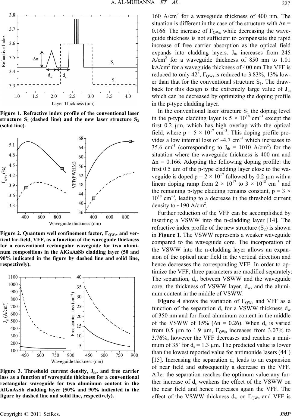
10–18 cm2 as found experimentally in [11]. Figure 1
shows the refractive index profile of the conventional
laser structure as structure S1. In this structure the com-
bination of a high refractive index step between the clad-
ding and the waveguide layers of n = 0.29 (correspond
to an aluminum content of 90% in the cladding layers
and 25% in the waveguide) and a broad-waveguide leads
to a small overlap of the optical mode with the cladding
layers and a high value for the overlap of the optical
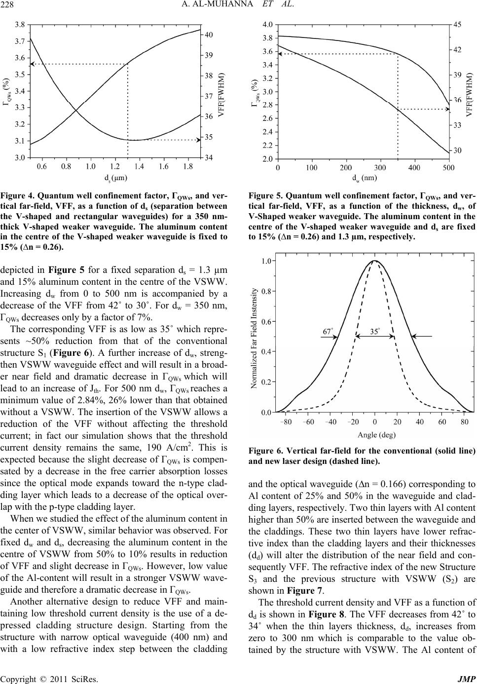
mode with the quantum wells. The variation of ΓQWs and
VFF as a function of the waveguide thickness is pre-
sented in Figure 2. The VFF has a value as high as 67˚
and ΓQWs = 4.4% for conventional laser structure S1 with
a total waveguide thickness of 850 nm. When the refrac-
tive index step is decreased in structure S1 to n = 0.166
(obtained by reducing the aluminum content to 50% in
the cladding layers) the VFF and ΓQWs decreases to 53˚
and 3.75%, respectively (Figure 2). Decreasing the wa-
veguide thickness is accompanied by an increase of the
threshold current density as a result of the increase of the
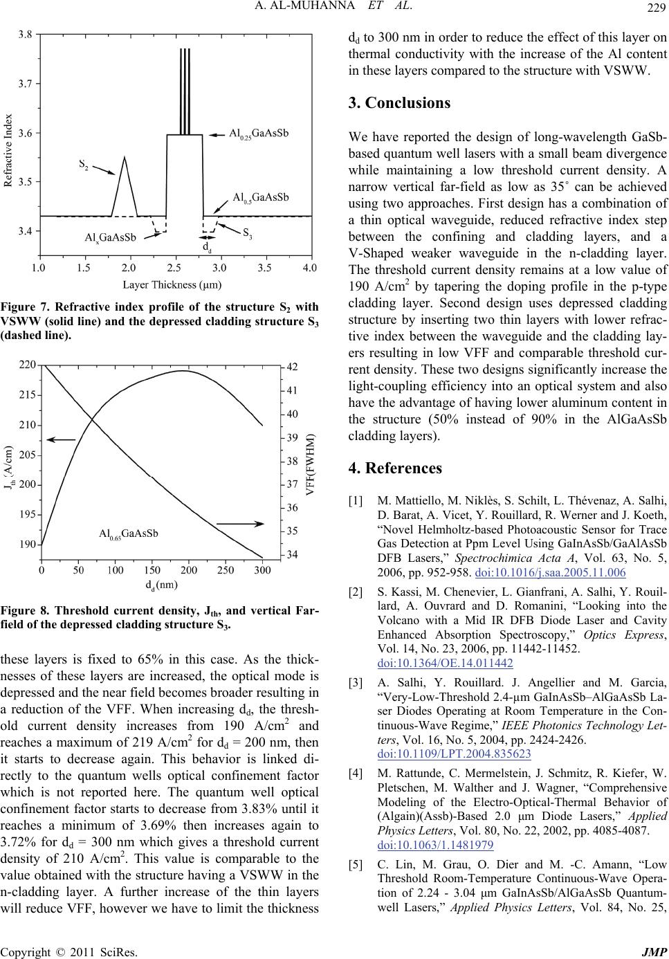
free carrier losses. This behavior is illustrated in Figure
3 in which we show the threshold current density and the
free carrier losses versus waveguide thickness for the
conventional structure with aluminum content of 50%
and 90% (n = 0.166 and 0.29, respectively). For both
structures, decreasing the waveguide thickness is ac-
companied by an increase of free carrier loss due to a
higher optical mode overlap with the p-type cladding
layer. Structures with a smaller index step between the
cladding and waveguide always possess higher
free-carrier losses regardless of the waveguide thickness
as shown in Figure 3. For the structure with n = 0.29
(S1), the threshold current density for 1000 × 100 µm2
laser is 135 A/cm2 (waveguide thickness of 850 nm) re-
mains constant until the waveguide thickness reaches
650 nm. This is due to the fact that the increase in free
carrier absorption is compensated by an increase of ΓQWs
(see Figure 2). Below a waveguide thickness of 650 nm
the threshold begins to increase and reaches a value of
Copyright © 2011 SciRes. JMP
A. AL-MUHANNA ET AL.
227
Figure 1. Refractive index profile of the conventional laser
structure S1 (dashed line) and the new laser structure S2
(solid line).
Figure 2. Quantum well confinement factor, ΓQWs, and ver-
tical far-field, VFF, as a function of the waveguide thickness
for a conventional rectangular waveguide for two alumi-
num compositions in the AlGaAsSb cladding layer (50 and
90% indicated in the figure by dashed line and solid line,
respectively).
Figure 3. Threshold current density, Jth, and free carrier
loss as a function of waveguide thickness for a conventional
rectangular waveguide for two aluminum content in the
AlGaAsSb cladding layer (50% and 90% indicated in the
figure by dashed line and solid line, respectively).
160 A/cm2 for a waveguide thickness of 400 nm. The
situation is different in the case of the structure with n =
0.166. The increase of ΓQWs while decreasing the wave-
guide thickness is not sufficient to compensate the rapid
increase of free carrier absorption as the optical field
expands into cladding layers. Jth increases from 245
A/cm2 for a waveguide thickness of 850 nm to 1.01
kA/cm2 for a waveguide thickness of 400 nm The VFF is
reduced to only 42˚, ΓQWs is reduced to 3.83%, 13% low-
er than that for the conventional structure S1. The draw-
back for this design is the extremely large value of Jth
which can be decreased by optimizing the doping profile
in the p-type cladding layer.
In the conventional laser structure S1 the doping level
in the p-type cladding layer is 5 × 1018 cm–3 except the
first 0.2 µm, which has high overlap with the optical
field, where p = 5 × 1017 cm–3. This doping profile pro-
vides a low internal loss of ~4.7 cm–1 which increases to
35.6 cm-1 (corresponding to Jth = 1010 A/cm2) for the
situation where the waveguide thickness is 400 nm and
n = 0.166. Adopting the following doping profile: the
first 0.5 µm of the p-type cladding layer close to the wa-
veguide is doped p = 2 × 10¹⁷ followed by 0.2 µm with a
linear doping ramp from 2 × 10¹⁷ to 3 × 1018 cm–3 and
the remaining p-type cladding remains constant, p = 3 ×
1018 cm–3, leading to a decrease in the threshold current
density to ~190 A/cm2.
Further reduction of the VFF can be accomplished by
inserting a VSWW into the n-cladding layer [14]. The
refractive index profile of the new structure (S2) is shown
in Figure 1. The VSWW represents a weaker waveguide
compared to the waveguide core. The incorporation of
the VSWW into the n-cladding layer allows an expan-
sion of the optical near field in the vertical direction and
hence decreases the corresponding VFF. In order to op-
timize the VFF, three parameters are modified separately:
The separation, ds, between VSWW and the waveguide
core, the thickness of VSWW layer, dw, and the alumi-
num content in the middle of VSWW.
Figure 4 shows the variation of ΓQWs and VFF as a
function of the separation ds for a VSWW thickness dw
of 350 nm and for fixed aluminum content in the middle
of the VSWW of 15% (n = 0.26). When ds is varied
from 0.5 µm to 1.9 µm, ΓQWs increases from 3.07% to
3.76%, however the VFF decreases and reaches a mini-
mum of 35˚ for ds = 1.3 µm. The predicted value is lower
than the lowest reported value for antimonide lasers (44˚)
[15]. Increasing the separation ds leads to an expansion
of near field and subsequently a decrease in the VFF.
After the separation reaches the optimum value any fur-
ther increase of ds weakens the effect of the VSWW on
the near field and hence increases again the VFF. The
effect of the VSWW thickness dw on ΓQWs and VFF is
Copyright © 2011 SciRes. JMP
228 A. AL-MUHANNA ET AL.
Figure 4. Quantum well confinement factor, ΓQWs, and ver-
tical far-field, VFF, as a function of ds (separation between
the V-shaped and rectangular waveguides) for a 350 nm-
thick V-shaped weaker waveguide. The aluminum content
in the centre of the V-shaped weaker waveguide is fixed to
15% (n = 0.26).
depicted in Figure 5 for a fixed separation ds = 1.3 µm
and 15% aluminum content in the centre of the VSWW.
Increasing dw from 0 to 500 nm is accompanied by a
decrease of the VFF from 42˚ to 30˚. For dw = 350 nm,
ΓQWs decreases only by a factor of 7%.
The corresponding VFF is as low as 35˚ which repre-
sents ~50% reduction from that of the conventional
structure S1 (Figure 6). A further increase of dw, streng-
then VSWW waveguide effect and will result in a broad-
er near field and dramatic decrease in ΓQWs which will
lead to an increase of Jth. For 500 nm dw, ΓQWs reaches a
minimum value of 2.84%, 26% lower than that obtained
without a VSWW. The insertion of the VSWW allows a
reduction of the VFF without affecting the threshold
current; in fact our simulation shows that the threshold
current density remains the same, 190 A/cm2. This is
expected because the slight decrease of ΓQWs is compen-
sated by a decrease in the free carrier absorption losses
since the optical mode expands toward the n-type clad-
ding layer which leads to a decrease of the optical over-
lap with the p-type cladding layer.
When we studied the effect of the aluminum content in
the center of VSWW, similar behavior was observed. For
fixed dw and ds, decreasing the aluminum content in the
centre of VSWW from 50% to 10% results in reduction
of VFF and slight decrease in ΓQWs. However, low value
of the Al-content will result in a stronger VSWW wave-
guide and therefore a dramatic decrease in ΓQWs.
Another alternative design to reduce VFF and main-
taining low threshold current density is the use of a de-
pressed cladding structure design. Starting from the
structure with narrow optical waveguide (400 nm) and
with a low refractive index step between the cladding
Figure 5. Quantum well confinement factor, ΓQWs, and ver-
tical far-field, VFF, as a function of the thickness, dw, of
V-Shaped weaker waveguide. The aluminum content in the
centre of the V-shaped weaker waveguide and ds are fixed
to 15% (n = 0.26) and 1.3 µm, respectively.
Figure 6. Vertical far-field for the conventional (solid line)
and new laser design (dashed line).
and the optical waveguide (n = 0.166) corresponding to
Al content of 25% and 50% in the waveguide and clad-
ding layers, respectively. Two thin layers with Al content
higher than 50% are inserted between the waveguide and
the claddings. These two thin layers have lower refrac-
tive index than the cladding layers and their thicknesses
(dd) will alter the distribution of the near field and con-
sequently VFF. The refractive index of the new Structure
S3 and the previous structure with VSWW (S2) are
shown in Figure 7.
The threshold current density and VFF as a function of
dd is shown in Figure 8. The VFF decreases from 42˚ to
34˚ when the thin layers thickness, dd, increases from
zero to 300 nm which is comparable to the value ob-
tained by the structure with VSWW. The Al content of
Copyright © 2011 SciRes. JMP
A. AL-MUHANNA ET AL.
229
Figure 7. Refractive index profile of the structure S2 with
VSWW (solid line) and the depressed cladding structure S3
(dashed line).
Figure 8. Threshold current density, Jth, and vertical Far-
field of the depressed cladding structure S3.
these layers is fixed to 65% in this case. As the thick-
nesses of these layers are increased, the optical mode is
depressed and the near field becomes broader resulting in
a reduction of the VFF. When increasing dd, the thresh-
old current density increases from 190 A/cm2 and
reaches a maximum of 219 A/cm2 for dd = 200 nm, then
it starts to decrease again. This behavior is linked di-
rectly to the quantum wells optical confinement factor
which is not reported here. The quantum well optical
confinement factor starts to decrease from 3.83% until it
reaches a minimum of 3.69% then increases again to
3.72% for dd = 300 nm which gives a threshold current
density of 210 A/cm2. This value is comparable to the
value obtained with the structure having a VSWW in the
n-cladding layer. A further increase of the thin layers
will reduce VFF, however we have to limit the thickness
dd to 300 nm in order to reduce the effect of this layer on
thermal conductivity with the increase of the Al content
in these layers compared to the structure with VSWW.
3. Conclusions
We have reported the design of long-wavelength GaSb-
based quantum well lasers with a small beam divergence
while maintaining a low threshold current density. A
narrow vertical far-field as low as 35˚ can be achieved
using two approaches. First design has a combination of
a thin optical waveguide, reduced refractive index step
between the confining and cladding layers, and a
V-Shaped weaker waveguide in the n-cladding layer.
The threshold current density remains at a low value of
190 A/cm2 by tapering the doping profile in the p-type
cladding layer. Second design uses depressed cladding
structure by inserting two thin layers with lower refrac-
tive index between the waveguide and the cladding lay-
ers resulting in low VFF and comparable threshold cur-
rent density. These two designs significantly increase the
light-coupling efficiency into an optical system and also
have the advantage of having lower aluminum content in
the structure (50% instead of 90% in the AlGaAsSb
cladding layers).
4. References
[1] M. Mattiello, M. Niklès, S. Schilt, L. Thévenaz, A. Salhi,
D. Barat, A. Vicet, Y. Rouillard, R. Werner and J. Koeth,
“Novel Helmholtz-based Photoacoustic Sensor for Trace
Gas Detection at Ppm Level Using GaInAsSb/GaAlAsSb
DFB Lasers,” Spectrochimica Acta A, Vol. 63, No. 5,
2006, pp. 952-958. doi:10.1016/j.saa.2005.11.006
[2] S. Kassi, M. Chenevier, L. Gianfrani, A. Salhi, Y. Rouil-
lard, A. Ouvrard and D. Romanini, “Looking into the
Volcano with a Mid IR DFB Diode Laser and Cavity
Enhanced Absorption Spectroscopy,” Optics Express,
Vol. 14, No. 23, 2006, pp. 11442-11452.
doi:10.1364/OE.14.011442
[3] A. Salhi, Y. Rouillard. J. Angellier and M. Garcia,
“Very-Low-Threshold 2.4-µm GaInAsSb–AlGaAsSb La-
ser Diodes Operating at Room Temperature in the Con-
tinuous-Wave Regime,” IEEE Photonics Technology Let-
ters, Vol. 16, No. 5, 2004, pp. 2424-2426.
doi:10.1109/LPT.2004.835623
[4] M. Rattunde, C. Mermelstein, J. Schmitz, R. Kiefer, W.
Pletschen, M. Walther and J. Wagner, “Comprehensive
Modeling of the Electro-Optical-Thermal Behavior of
(Algain)(Assb)-Based 2.0 μm Diode Lasers,” Applied
Physics Letters, Vol. 80, No. 22, 2002, pp. 4085-4087.
doi:10.1063/1.1481979
[5] C. Lin, M. Grau, O. Dier and M. -C. Amann, “Low
Threshold Room-Temperature Continuous-Wave Opera-
tion of 2.24 - 3.04 μm GaInAsSb/AlGaAsSb Quantum-
well Lasers,” Applied Physics Letters, Vol. 84, No. 25,
Copyright © 2011 SciRes. JMP
A. AL-MUHANNA ET AL.
Copyright © 2011 SciRes. JMP
230
2004, pp. 5088-5090. doi:10.1063/1.1760218
[6] D. Z. Garbuzov, R. U. Martinelli, H. Lee, P. K. York, R.
J. Menna, J. C. Connolly and S. Y. Narayan, “Ultralow-
loss Broadened-Waveguide High-Power 2 μm Al-
GaAsSb/InGaAsSb/GaSb Separate-Confinement Quan-
tum Well Lasers,” Applied Physics Letters, Vol. 69, No. 7,
1996, pp. 2006-2008. doi:10.1063/1.116861
[7] J. G. Kim, L. Shterengas and G. L. Belenky, “High-
Power Room-Temperature Continuous Wave Operation
of 2.7 and 2.8 μm In(Al)GaAsSb/GaSb Diode Lasers,”
Applied Physics Letters, Vol. 83, No. 10, 2003, pp. 1926-
1928. doi:10.1063/1.1605245
[8] J. Devenson, O. Cathabard, R. Tessier and A. N. Baranov,
“InAs/AlSb Quantum Cascade Lasers Emitting at
2.75-2.97 μm,” Applied Physics Letters, Vol. 91, No. 25,
2007. doi:10.1063/1.2825284
[9] J. Devenson, O. Cathabard, R. Tessier and A. N. Baranov,
“High Temperature Operation of λ~3.3 µm Quantum
Cascade Lasers,” Applied Physics Letters, Vol. 91, 2007.
doi:10.1063/1.2794414
[10] L. Shterengas, G. L. Belenky, T. Hosoda, G. Kipshidze
and S. Suchalkin “Continuous Wave Operation of Diode
Lasers at 3.36 μm at 12˚C,” Applied Physics Letters, Vol.
93, 2008.
[11] M. Rattunde, J. Schmitz, R. Kiefer and J. Wagner,
“Comprehensive Analysis of the Internal Losses in 2.0
μm (AlGaIn)(AsSb) Quantum-Well Diode Lasers,” Ap-
plied Physics Letters, Vol. 84, No. 23, 2004, pp. 4750-
4752. doi:10.1063/1.1760216
[12] A. Salhi and A. Al-Muhanna, “Self Consistent Analysis
of Quantum Well Number Effects on the Performance of
2.3 μm GaSb-Based Quantum Well Laser Diodes,” IEEE
Journal of Selected Topics in Quantum Electronics, Vol.
15, No. 3, 2009, pp. 918-924.
doi:10.1109/JSTQE.2008.2012000
[13] FIMMWAVE and HAROLD by Photon Design
http://www.photond.com
[14] B. Qiu, S. S. McDougall, X. Liu, G. Bacchin and J. H.
Marsh, “Design and Fabrication of Low Beam Diver-
gence and High Kink Free Power Lasers,” IEEE Journal
of Quantum Electronics, Vol. 41, No. 9, 2005, pp. 1124-
1130. doi:10.1109/JQE.2005.853359
[15] M. T. Kelemen, J. Weber, M. Rattunde, G. Kaufel, J.
Schmitz, R. Moritz, M. Mikulla and J. Wagner, “High
Power 1.9 μm Diode Laser Arrays with Reduced
Far-Field Angle,” IEEE Photonics Technology Letters,
Vol. 18, No. 4, 2006, pp. 628-630.
doi:10.1109/LPT.2006.870146