Journal of Computer and Communications, 2013, 1, 40-45
Published Online December 2013 (http://www.scirp.org/journal/jcc)
http://dx.doi.org/10.4236/jcc.2013.17010
Open Access JCC
Study on the Luminescence Properties of the Strain
Compensated Quantum Well*
Tao Liu, Jianjun Li#, Jiachun Li, Jun Han, Jun Deng, Linjie He, Shengjie Lin
Key Laboratory of Opto-Electronics Technology, Beijing University of Technology, Beijing, China.
Email: liutao2011@emails.bjut.edu.cn, #lijianjun@bjut.edu.cn
Received September 2013
ABSTRACT
Compared with the conventional strained quantum well, the InGaAs/GaAsP strain compensated quantum well (SCQW)
has better optical properties, as the well layer and th e barrier layer lattice mismatch with each other which result s in the
introduction of stress. In this paper, we adopted the Kohn-Luttinger Hamiltonian, conducted some theoretical calcula-
tions using the transfer matrix method, and finally verified the following change trend of the InGaAs quantum well fol-
lowing the In-group through experiments: the growth of the low In-group can improve the epitaxial flatness of the ac-
tive area; the growth of the high In-group can increase the wavelength as well as the strain. In this paper, we adopted
the AlGaAs barrier material instead of the GaAsP, made an analysis on the level changes of the compensation quantum
well, and successfully fostered the strain compensated quantum well structure using the metal-organic chemical vapor
deposition (MOCVD) system which ha d better optical properties compared with the strained quantum wells.
Keywords: InGaAs/AlGaAs; InGaAs/GaAsP; Strain Compensated Quantum Well; MOCVD
1. Introduction
InGaAs is an important semiconductor material, whose
carrier mobility is more than 10 times compared with the
ordinary Si material. InGaAs has many potential applica-
tions in the new generation of optical fiber communica-
tion and lasers. The high-quality strained InGaAs quan-
tum wells have been widely used in the optoelectronic
devices. The laser performance [1,2] can be greatly im-
proved by adopting the strained quantum well structure
in the active layer.
When design the large optical cavity (LOC) high-
power lasers, high-quality quantum wells grown is our
key consideration and the design of the InGaAs/AlGaAs
strained quantum wells is the focus of the design direc-
tion. Ho wev er , as th e cr it ica l s train th ic kn e ss of the strained
quantum well is small, it is difficult to release stress. In
the growth process of high In composition, the lattice
defects may lead to the design limitations of the long
wavelength.
In the strain compensated structure, the barrier layer
adopts the GaAsP which has an opposite strain with the
well layer. Therefore, the above mentioned shortcomings
[3] can be well overcame. Moreover, Dutta et al. [4]
found through exp eriments that the gain of the lasers can
be improved by adopting the InGaAs/GaAsP strain com-
pensated qua ntum wells inste ad of s trained quantum wells.
GaAsP an d AlG aAs hav e a similar band gap, wh ile GaAsP
has a smaller lattice constant. The tensile stress subjected
in the quantum wells compensates with the compressive
resistance of the InGaAs potential well, which can great-
ly improve the stress properties of material growth.
By adopting the In0.2Ga0.8As quantum wells which is
of 8 nm LP-MOVCD thick growth, the AlGaAs and the
GaAsP are selected as the barrier materials. Theoretical
and experimental validation show that the stress of the
InGaAs/AlGaAs strain ed quantum well grown in the GaAs
substrate has increased rapidly and the critical thickness
thereof has decreased rapidly. The wavelength is limited
in a certain range and the long-wavelength components
can’t be made. The InGaAs/GaAsP strain compensated
quantum wells can effectively alleviate the impact of stress.
Through theoretical analysis and PL spectra measure-
ments, the impact of the quantum wells stress on spec-
trum is verified.
Through theoretical analysis on th e well width and the
barrier material trends of the energy band structure in
quantum wells, and comparative analysis of the InGaAs/
AlGaAs strained quantum well and InGaAs/GaAsP strain
compensated quantum wells, we can see that compared
*Supported by the Advanced Technology F u
nd of Beijing University of
Technology und er Grant No. 0020005143 1 2003.
#Correspondi ng author.
Study on the Luminescence Properties of the Strain Compensated Quantum Well
Open Access JCC
41
with the strained quantum well, the strain compensated
quantum wells have better luminescence properties.
2. Experimental Methods
We adopted the Emcore D125 LP-MOCVD system and
conducted the epitaxial growth of the material, wherein
the growth conditions are as follows: the pressure is 80
mbar; the substrate carrier speed is 1000 r/s, the palla-
dium tube purified H2 is adopted as the carrier gas; the
flow rate is 30 slm, the adopted V group source is the
high purity AsH3; the III group source are TMAl, T MGa
and TMIn.
We conducted epitaxial growth in accordance with ep-
itaxial structure in Table 1. We adopted the no-clean
GaAs semi-insulating substrate. The substr ate orientation
is (100) biased (111) 2˚. The grown sequence are GaAs
buffer layer, n-type confinement layer, waveguide layer,
quantum wells, barrier layer, quantum well, upper wave
guide layer, p-cladding layer, covering layer.
As shown in Table 2 , we prepared four different sam-
ples. The first two samples are InGaAs/AlGaAs strained
quantum well structure. The last two samples are In-
GaAs/GaAsP strain compensated quantum wells. In the
growth process, In with different traffic were flowed into
the four samples, wherein the traffic volume are as fol-
lows: No 1:126.7 cm3; No 2: 101.7 cm3; No 3:126.7 cm3;
No 4: 101.7 cm3.
Table 1. Quantum well growth parameters design.
Layer Composition Width (nm)
1 GaAs coating 5
2 Al0.3Ga0.7As p-cladding layer 200
3 Al0.1Ga0.9As n-waveguide layer 200
4 barrier 20
5 InGaAs well 20
6 barrier 8
7 InGaAs well 200
8 barrier 20
9 Al0.1Ga0.9As n-waveguide layer 200
10 Al0.3Ga0.7As n-cladding layer 300
11 GaAs buffer layer 200
12 GaAs substrate
Table 2. Barrier growth parameters of the four samples.
Sample In flow (cm3) Barrier material
1 126.7 AlGaAs
2 101.7 AlGaAs
3 126.7 GaAsP
4 101.7 GaAsP
3. Theoretical Calculations
In order to explore the stress of the quantum well, we
have checked the relevant material properties [6], in-
cluding the lattice constant, elastic modulus, hydrostatic
pressure and shear deformation potential, etc. We have
conducted some theoretical calculations by using these
parameters. And then we got the change rules of the
quantum well band gap following the stress, which have
given the theoretical support for our experiment.
InGaAs/AlGaAs strained quantum well band gap is
subject to the following three aspects:
1) The In components may result in the InGaAs ma-
terial band gap changes [7];
2
( )1.4241.6140.54
g
Exx x=−+
(1)
2) The thickness of the well material is thin enough to
be comparable with the De Buluo intended wavelength
(1 ~ 50 nm), which result in the Quantum Size Effect
[8,9]. The energy level can be split into a series of values:
E1, E2, E3, ..., En.
3) The strain may result in the overall movement of
the bottom and top of conduction band, and the separa-
tion of heavy and light holes.
As shown in Figure 1, the potential well material In-
GaAs, and the barrier materials AlGaAs and GaAsP were
respectively used to prepare the strained quantum wells
and strain compensated quantum wells. As for the strained
quantum well, the barrier band gap structure will not
vary with strain changes of the potential well. As the
lattice matches with the substrate, the barr ier can grow to
a very large thickness, which has reduced the difficulty
of the epitaxial growth. As for the strain compensated
quantum wells, the introduction of the GaAsP material
which does not match the substrate lattice may result in
the restriction of the grown thickness. In order to reduce
the lattice defects resulting from the dismatch, our Al and
P compone nt s are 0. 1 with the thi c kness of 20 nm.
According to the literature [10] calculation method, we
use the Kohn-Luttinger Hamiltonian to solve the quan-
tum wells strain effect. By adopting this approach, we
need to solve a 4 × 4 matrix. Through unitary transfor-
mation, we need to solve a 2 × 2 matrix calculation. By
adopting the transfer matrix method, we can get a credi-
ble theoretical solution.
0
0
U
L
H
HH

=

(2)
Wherein, the HU and HL are both 2 × 2 matrix.
As for the strained quantum well, the Hamiltonian is:
()
h
PQ R
H Vz
R PQ
ζ
ζ
 ++

= +


−−


(3)
Wherein,
Study on the Luminescence Properties of the Strain Compensated Quantum Well
Open Access JCC
42
j=12 3456789
d
1
d
3
d
4
d
5
d
6
d
7
d
8
d
2
(GaAsP)
AlGaAs In
x
Ga
1-x
As
a(x)
-ζ
LH +ζ
ΔE
c
ΔE
v
HH
AlGaAs AlGaAsAlGaAs
(GaAsP)
In
x
Ga
1-x
As In
x
Ga
1-x
As In
x
Ga
1-x
AsAlGaAs
δE
c
E
g
B
δE
v
E
g
(x)
(GaAsP) (GaAsP)(GaAsP)
Figure 1. The e nergy-band diagram in real space.
(4)
Through analysis of the continuous wave function, we
use the matrix Uj(j+1) to represent the relationship between
adjacent layers,
( 1)
( 1)( 1)
HHjHH j
jj
HHjHH j
AA
U
BB
+
+
+
 
=
 
 
(5)
By adopting the transfer matrix method, we obtained
the Ut, and then the solution of Ut can be gotten,
( 1)
11223( 1)( 1)
1
HH j
HH jj HH j
HH
A
AUU UB
B
+
+
+


=⋅⋅⋅ 

 
(6)
11 12
1223( 1)21 22
t jj
uu
U UUUuu
+

=⋅⋅⋅= 

(7)
Wherein,
( 1)1
( 1)1
( 1)( 1)
( 1)( 1)( 1)
11 0
111
20
i zj
i zj
ik l
jj jj
jj ik l
jj jj
pp
e
Upp e
++
++
++
+
++

+−

=

−+



(8)
( 1)
( 1)1
jjz
jj j jz
mk
pmk
+
+
+
=
(9)
2
2
12
1[( )]
()
2
zh
kE Vz
h
m
ζ
γγ
= +−
+
(10)
By calculating the solution of u11 = 0, we obtained E.
As the existence of the quantum size effect, we got a
series of solutions: E1, E2, E3, ..., En. They are corres-
ponding to the different energy levels. The boundary
condition determines that they can not exceed the poten-
tial barrier height. The fact of the energy splitting result-
ing from the strain was also verified theoretically. As
shown in Figures 2, and 3, the a, b, c in Figure 2 are th e
change trend of the wavelength along with the In compo-
sition and well width, which respectively represents the
change trend of the wavelength of the strained quantum
well conduction band energy, the amount of heavy-hole
band, and between the nearest energy levels. Figure 3
shows the corresponding strain compensated quantum
wells. By comparison, we found that the change trend of
the energy band of the barrier material adopting the
Al0.1Ga0.9As and Ga0.9AsP0.1 is consistent with the change
trend of the transition wavelength.
As for the strain compensated quantum wells, when
the thickness of the well layer (8 nm) is the same with the
In component (0.2). Compared with the strained quantum
well, the compensated quantum wells have introduced
the tensile stress in the barrier material. The tensile s tress
served as Interaction force and acted on the potential well
layer. The additional stress caused the reduction of the
effective mass of the heavy hole. Due to the reduction of
the heavy hole effective mass, the variation volume of
the band gap resulting from the quantum size effect may
increase, which finally resulting in an increase of the
effective band gap and the blue shift of the wavelength.
We can clearly find that this phenomenon in the follow-
ing experiment. As the theoretical analysis model is a b it
complex, we only conduct qualitative analysis here. We
can also see the properties in the researches made by
Duraev et al. [11].
4. Results and Analysis
After the text edit has been completed, the paper is ready
for the template. Duplicate the template file by using the
Save As command, and use the naming convention pre-
scribed by your journal for the name of your paper. In
Study on the Luminescence Properties of the Strain Compensated Quantum Well
Open Access JCC
43
Figure 2. Change of the InGaAs/GaAsP strained quantum
well energy following the In-group and the potential well
width. a is the first heavy-hole band; b is the first conduc-
tion band, c is the energy level transition wavelengths be-
tween the first heavy-hole band and the conduct i on ban d.
Figure 3. Change of the InGaAs/GaAsP strained compen-
sated quantum well energy following the In-group and the
potential well width. a is the first heavy-hole band; b is the
first conduction band, c is the energy level transition wave-
lengths between the first heavy-hole band and the conduc-
tion band.
this newly created file, highlight all of the contents and
import your prepared text file. You are now ready to style
your pape r .
Under the same environmental conditions (300 K), we
conducted unified tests for the four samples. The test
equipment is the Philips PLM100 type PL test system.
Test results ar e shown in Table 3. The In flow of sample
1 is 126.7 cm3, the corresponding component is 0.2, and
the luminescence center wavelength is 962 nm. Because
of the parameter control error resulting from the labora-
tory equipment, compared with the theoretical results,
there is still a certain wavelength deviation.
The above theoretical studies have shown that the cen-
tral wavelength is mainly affected by three parts: First,
the InGaAs material changes resulting form the In com-
position. As the decrease of the In composition, the band
gap of the quantum well material may increase; Second,
due to the change of the stress, the conduction band will
increase and the light and heavy holes may separate, and
the band gap may change. As the increase of the In
composition, the InGaAs lattice constant may increase,
the well material stresses may also increase, the bottom
of the conduction band and the top of valence band may
decrease, the heavy and light hole may separate, the band
gap may increase, and the wavelength may have a blue
shift; Third, the narrow quantum well may result in width
effect as well as a energy level split of the potential well.
Through study of the No 1 and No 3 samples, we can
conduct qualitative analysis o f the impact of the stre ss on
the quantum wells. Sample No. 1 and No 3 are of the
same In flow rate: 126.7 cm3. The No 3 Sample is the
InGaAs/GaAsP strain compensated quantum wells. As
the lattice constant of the GaAs0.9P0.1 barrier (5.6331 Å)
is less than the lattice constant of the GaAs substrate
(5.6533 Å), the barrier layer will subjec t to tensile strain.
The tensile strain stress, as the interaction force, will act
on the InGaAs well layers. The InGaAs well layers are
inherently subjected to the compressive stress. The oppo-
site stress of the barrier and the well compensate each
other, to promote more uniform stress, which can greatly
improve the stability of the quantum well. Due to the
increase of the internal stress, the separation of light and
heavy hole band may also increase. After comparison
with the strained quantum well, we find that the center
wavelength has a blue shift. From Figure 4, we can
Table 3. Measurements of the four samples of photolumi-
nescence (PL).
Sample Peak wavelength
(nm) Light intensity
(AU*) Half peak width
(nm)
1 962.0 3176.1 22.1
2 928.0 3870.8 20.1
3 952.0 4571.4 23.5
4 912.0 4986.4 18.2
0 2 4 6 810 12 14
-0.04
-0.02
0
0.02
0.04
well width (nm)
Energy (eV)
a HH10.25
0.2
0.15
0.1
x
0246810 12 14
0.05
0.1
0.15
0.2
0.25
0.3
0.35
0.4
well width (nm)
Energy (eV)
b C1
0.2
0.25
0.15
x
0.1
0 2 46810 1214
800
850
900
950
1000
well width (nm)
wavelengt h (nm )
c C 1 - HH10.25
0.2
0.15
0.1
x
024681012 14
-0.04
-0.02
0
0.02
0.04
well width (nm)
Energy (eV)
a HH1
0.1
x
0.25
0.2
0.15
0246810 1214
0.1
0.2
0.3
0.4
0.5
well width (nm)
Energy (eV)
b C1
0.15
x
0.25
0.2
0.1
0 246810 1214
800
850
900
950
1000
well width (nm)
wavelengt h (nm )
c C 1 - HH1
x
0.25
0.2
0.15
0.1
Study on the Luminescence Properties of the Strain Compensated Quantum Well
Open Access JCC
44
850900950 1000
0
1000
2000
3000
4000
5000
43
2
Intensit y(AU*)
Wavelength(nm)
S am ple 1
S am ple 2
S am ple 3
S am ple 4
1
SCQW
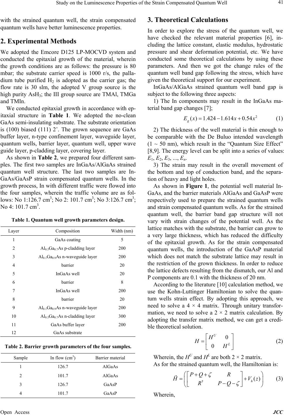
Figure 4. Photoluminescence of four samples.
clearly see that the No. 3 sample has an obvious blue
shift compared with No 1, reaching 10 nm.
Based on the study of the four samples, we find that as
the In composition decreases, the strained quantum wells
and the strain compensated quantum wells, the peak half-
width may reduce accordingly. As the decrease of the In
component, the decrease of the lattice fit of the quantum
well, the decrease of the corresponding stress, the de-
crease of the defects in the epitaxial growth process, and
the increase of the flatness of the epitax ial layer, the light
intensity can be effectively improved and the peak half
width can be reduced. Therefore, the growth of the low
In composition can improve the epitaxial growth of the
active region.
Affect the optical properties of quantum wells factors
on the one hand the strained quantum well type, the epi-
taxial growth proce ss on the o ther hand .
After comparison of the No 1 and No 3 sample and
comparison of the No 2 and No 4 sample, we found that
the fluorescenc e intensity of the strain comp ensated quan-
tum wells can be significantly improved on the basis of
strained quantum well. This kind of improvement can not
be fully explained by the strain mechanism. The strained
quantum well barrier materials adop t the AlGaAs. As the
Al is of high chemical activity, it can easily react with O
impurities and then generate the Al-O bond. The incor-
poration of the O impurities may lead to the non-radia-
tive recombination centers, which can greatly reduce the
fluorescence intensity [12]. In contrast, the strain com-
pensated quantum well adopts the GaAsP materials. The
application of materials without Al can reduce the incor-
poration of the O impurities, which can effectively im-
prove the fluorescence intensity.
5. Summary
We prepared four kinds of samples under the same con-
ditions. The theoretical calculation and the experimental
demonstration have verified the affecting factors of the
characteristics of luminescen ce for the qu antum well. This
paper has focused on analysis of the stress on the optical
properties of quantum we lls. Due to t he c ompressi ve stress,
the wavelength of the fluorescence luminescence center
may have a blue shift. The adoption of the growth of the
In composition, the stress of the potential well layer may
decrease, which may greatly improve the epitaxial flat-
ness of the well layer. The barrier material adopts the
GaAsP material, and InGaAs strain compensated quan-
tum well structure is prepared. The stress compensation
and properties of the without Al can greatly increase the
optical properties of quantu m wells.
REFERENCES
[1] J. V. Moloney, J. Hader and S. W. Koch, “Quantum De-
sign of Semiconductor Active Materials Laser and Am-
plifier Applications,” Laser & Photonics Reviews, Vol. 1,
2007, pp. 24-43.
http://dx.doi.org/10.1002/lpor.200610003
[2] J. Hader, J. V. Moloney, M. Fallahi, et al., “Closed-Loop
Design of a Semiconductor Laser,” Optics Letters, Vol.
31, No. 22, 2006, pp. 3300-3302.
http://dx.doi.org/10.1364/OL.31.003300
[3] H. Toktamis, B. Gonul and M. Oduncuoglu, “Compara-
tive Study of the Band-Offset Ratio of Conventionally
Strained and Strain Compensated InGaAs/GaAs QW La-
sers,” Physica E, Vol. 24, 2004, pp. 183-186.
http://dx.doi.org/10.1016/j.physe.2004.03.020
[4] N. K. Dutta, W. S. Hobson, D. Vakhshoori, et al., “Strain
Compensated In-GaAs-GaAsP-InGaP Laser,” IEEE Pho-
tonics Technology Letters, Vol. 8, No. 7, 1996, pp. 852-
854. http://dx.doi.org/10.1109/68.502248
[5] A. Moser, A. Oosenbrug, E. E. Latta, Th. Forster and M.
Gasser, High-Power Operation of Strained InGaAs/Al-
GaAs Single Quantum Well Lasers,” Applied Physics
Letters, Vol. 23, 1991, pp. 2642-2644.
http://dx.doi.org/10.1063/1.105924
[6] P. K. Bhattacharya, “Semiconductor Optoelectronic De-
vices,” Pearson Education, US, 1996.
[7] R. M. Kolbas, N. G. Anderson, W. D. Ladig, et al., IIEEE
Journal of Quantum Electronics, QE, Vol. 24, No. 8,
1998, p. 1605.
[8] S. L. Chuang, Physics of Optoelectronic Devices,” Wi-
ley, New York , 1995.
[9] L. A. Coldren and S. W. Corzine, “Diode Lasers and Pho-
tonic Integrated Physics,” Wiley, Ne w Yor k , 1995.
[10] S. L. Chuang, “Efficient Band-Structure Calculations of
Strained Quantum Wells,” Physical Review, Vol. B43,
1991, pp. 9649-9661.
[11] V. P. Duraev, A. A. Mamalyuk, A. A. Padalitsa, et al.,
Effect of GaAsP Barrier Layers on the Parameters of
InGaAs/AlGaAs Laser Diodes Emitting in the 1050~1100
nm Spectral Range,” Quantum Electronics, Vol. 35, No.
Study on the Luminescence Properties of the Strain Compensated Quantum Well
Open Access JCC
45
10, 2005, pp. 909-911.
http://dx.doi.org/10.1070/QE2005v035n10ABEH005742
[12] D. C. Lu and S. K. Duan, “Principles and Applications of
Metal Organic Vapor Phase Epitaxy,” Science Press, Bei-
jing, 2009, pp. 160-164. (in Chinese)