Wireless Sensor Network
Vol.4 No.6(2012), Article ID:19703,4 pages DOI:10.4236/wsn.2012.46025
A 2.4-GHz-Low-Power CMOS RF Transmitter for IEEE 802.15.4 Standard
Laboratory of Micro-Optoelectronics and Nanostructures (LMON), Faculty of Sciences of Monastir, Boulevard de L’environnement, Monastir, Tunisia
Email: {nasrimohsen, amina.msolli}@yahoo.fr, abdelhamid.helali@isimm.rnu.tn, hassen.maaref@fsm.rnu.tn
Received April 7, 2012; revised May 12, 2012; accepted May 29, 2012
Keywords: IEEE 802.15.4 Transmitter; CMOS; Low Cost; Low Power; Wireless Sensor Network
ABSTRACT
This paper presents the experimental results of a low-power RF transmitter for 2.4-GHz-band IEEE 802.15.4 standard in 0.18-µm CMOS technology. In order to make an adaptive RF transmitter, several factors must be considered. The most important factors are performances, power consumption, output power, noise factor, and cost. The RF transmitter comprises a quadrature passive mixer, and a power amplifier. The proposed RF transmitter consumes only 10.8-mW under a supply voltage of 1.8-V.
1. Introduction
Recently, the growth of single-chip ultra low-power CMOS transceivers for the 2.4-GHz-band has been increasing significantly with the birth of the IEEE 802.15.4 standard [1]. This standard demands a longer battery life and lower-cost solutions for applications. The IEEE 802.15.4 standard refers to the large-scale deployment of small, inexpensive, and battery-powered sensing devices called sensor node with on-board processing and wireless communication capabilities which achieve a self-organized, infrastructure-less, and fault-tolerant sensor network in a cooperative way. Using such network, three operating frequency bands are considered: 868-MHz band in European, 915-MHz band in America, and the 2.4- GHz-band globally. There are three possible data rate of the IEEE 802.15.4 standard depending on the operating frequency band: 20 kb/s, 40 kb/s and 250 kb/s. This standard is being deployed over long periods of time in a wide range of potential applications scenarios, including automation, industrial, consumer electronics, personal health care, and chemical or biological phenomena. Of course, energy conservation is a fundamental concern for achieving the required network lifetime since battery replacement of sensor nodes is often impossible.
The radio subsystem is one of the most power consuming parts in sensors node. This unit consumes more than 50% during data communication. Our preliminary study on the design of a Radiofrequency Front-End module for WSN shows that the transmitter unit is one of the most powers hungry of the transceiver component of sensor nodes as depicted in Figure 1. By optimizing power consumption of this unit, performance and energy requirements of the entire RF parts can be significantly improved. For this reason, we target the transmitter design step to minimize the energy consumption.
In this paper, we will describe the design and implementation of low-power CMOS RF transmitter for 2.4- GHz-band IEEE 802.15.4 standard. With the main goal of low power, low noise, and high linearity, the solution we are presenting is the use of a quadrature passive mixer operating in the current mode followed by a power amplifier (PA) [2].
The rest of the paper is organized as follows. In Section 2, we examine related work. The transmitter design is described in Section 3. Simulation results are shown in Section 4. We conclude the paper in Section 5.
2. Related Work
In the last decade, there are several CMOS-based 2.4- GHz low-power transceivers related to the IEEE 802.15.4 standard [3]. But, those works are not always energy efficient for the IEEE 802.15.4 applications. However, those related research efforts still dissipate quite high power consumption. Thus, it is desirable to minimize the power dissipation. To address the above mentioned concerns, the most common solution is to employ a current reused technique [4]. Using the current reused technique, the linearity is limited due to the stack of several transistors.
This solution is based on different transceiver archi-
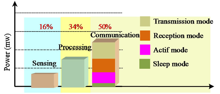
Figure 1. Distribution of energy consumption in sensing, processing and communication.
tectures. The transceiver design related to wireless sensor network applications are classified in a three categories: 1) super-heterodyne; 2) low-intermediate frequency (lowIF); and 3) direct conversion [5]. The super-heterodyne architecture requires several mixers; therefore, it leads to greater power and makes the transceiver implementation more complicated. The low-IF architecture is characterized by a high analog-to-digital conversion (ADC) sampling rate leading higher power consumption [6]. In the direct-conversion architecture, a minimum number of external components is used such as the image rejection filter which is not needed and the IF bandpass filter is replaced by the low-pass filter. Therefore, this architecture is suitable for low-power and low-cost applications.
In this design, considering a low-cost and low-power aspect, the direct-conversion architecture is considered. This architecture is attracting by the easy integration with the baseband circuit, as well as its low power consumption and low manufacturing costs. In the transmitter chain, the image signals rejection is taken into account by using the low-IF receiver. This architecture uses 90˚ phases shifter in the signal path that introduces the limitation in the signal bandwidth, since the phase shifter is inherently narrow band. The considered transmitter consists of a quadrature passive mixer and a low-noise power amplifier.
Using this architecture, the IEEE 802.15.4 applications have a very low duty cycle of use. Therefore, it’s essential to reduce both their consumption in operation mode and in sleep mode. For the latter mode, the power consumption should be less than 1 μA. Therefore, a minimum number of external components and a small silicon surface are critical to reduce the cost of such circuits.
3. The Transmitter Design
The proposed transmitter front-end is shown in Figure 2. It consists of a power amplifier (PA), and a passive upconversion mixer with an O-QPSK digital modulation. In the direct-conversion transmitter, an LO leakage to the RF out port is one of the main drawbacks. In the upconversion mixer, the LO leakage is caused by either the mismatches in input signal or the mismatches in the DC current between two differential branches in the switching pair. To solve this problem, a conventional passive mixer dissipating no dc current is adopted [7].
In this architecture, an output RF signal of the upconversion mixer is then amplified by a conventional cascode power amplifier topology with an additional capacitor C1 as shown in Figure 3. The function of the power amplifier is to provide a transmitted signal with an appropriated output power. A capacitor is added to the gate-source terminal of an input transistor M1 to keep the input signal linear since the intrinsic gate-source capacitance Cgs, which is essentially a bias dependent varactor, may lead to significant distortion at high input power levels [8]. The input transistor is biased at a high gatesource voltage to operate in class-A mode. The loading of the amplifier is chosen by considering the voltage and current swing at this node [9]. The total current consumption of the proposed amplifier is 6-mA under a supply voltage of 1.8-V.
The power cascode topology is chosen for the following reasons:
• Due to the greater power margin, the linearity should be improved.
• The gain can be controlled by varying the DC current of the pMOS transistor by changing the DC voltage to the cascode transistor gate.
Using the proposed PA, the network L1 – C1 eliminates the strong second harmonic of the carrier, while the network
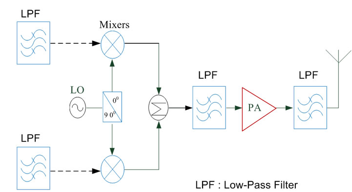
Figure 2. The block schematic of the transmitter RF.
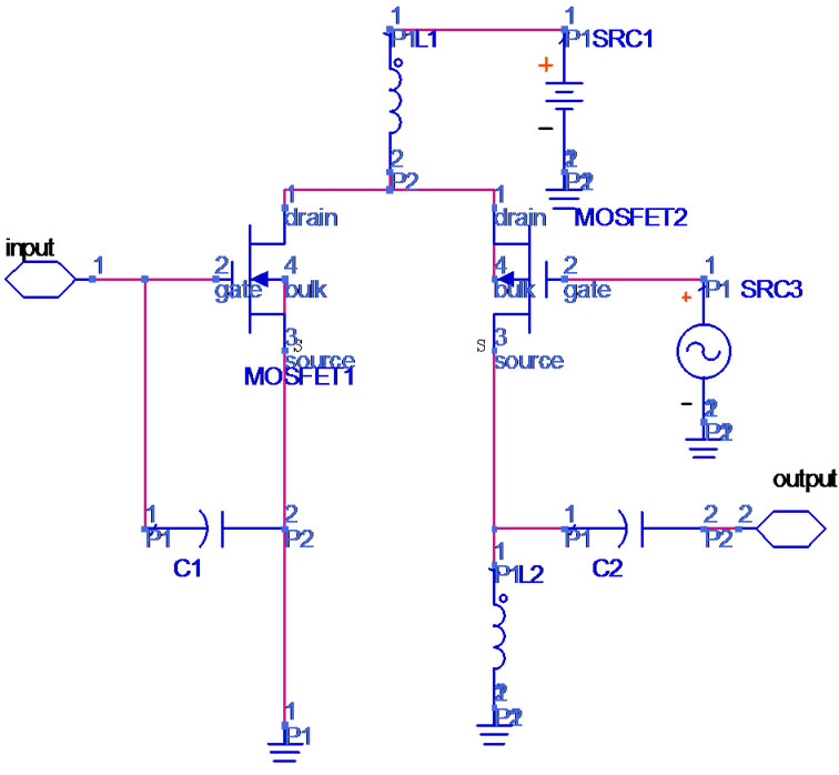
Figure 3. The power amplifier.
L2 – C2 is tuned to carrier frequency. The input impedance of the proposed PA is given by
 (1)
(1)
where, Cgs is gate-source capacitor of the transistor M1.
The network L2 – C2 is used also to adapt the output impedance to 50-Ω.
4. Simulation Results and Discussions
The proposed circuit is simulated with ADS simulation tools in 0.18-µm CMOS. The circuit is designed for 2.4- GHz ISM frequency band using the 2.4 - 2.48 GHz bandwidth. The transmitter dissipates 6-mA from a 1.8-V supply. S-parameters of the power amplifier have been shown in Figure 4. Both of input and output matching are good in the desired IF frequency (IF = 6-MHz). From Figure 4, it can be seen that the input and output impedance of the proposed PA are well adopted at 2.4-GHz which is a goal in the study.
Since the sensor network will be used for some critical sensing application, the transmission reliability is evaluated by the output power signal. Figure 5 depicts a maximum output power of 1.7-dBm with an input power of 0- dBm.
The results show that the proposed architecture reduces significantly the power consumption with sufficient a transmitter output power.
The comparison of the results in this study with those of other works is given in Table 1. As can be seen in Table 1, this work has low power dissipation while still achieving relatively good performances compared with the others.
 (a)
(a)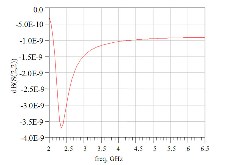 (b)
(b)
Figure 4. S-parameters: (a) Input return loss (S11); (b) Reverse isolation (S22).
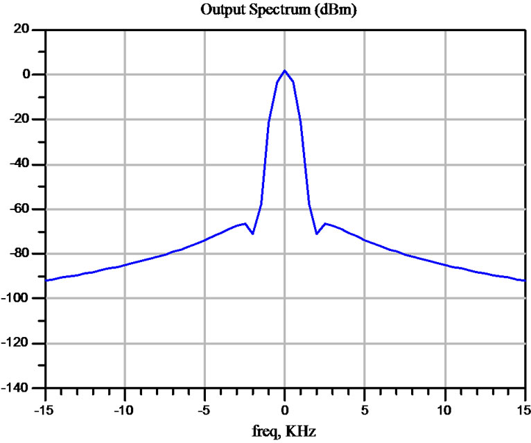
Figure 5. Output power of the proposed transmitter.
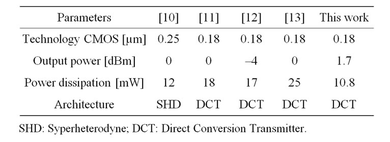
Table 1. Performances comparison.
5. Conclusion
In this paper, a low-power low-cost direct conversiontransmitter for the 2.4-GHz-band IEEE 802.15.4 standard was presented. Then, the specifications for power amplifier module in the transmitter were assigned, which is the sensitive module. The proposed transceiver was fabricated using 0.18-μm CMOS technology with a supply voltage of 1.8-V. The power amplifier showed a PEA (Power Added Efficiency) of 38% and dissipated 9-mW. In the whole transmitter chain, 1.7-dBm output power and 3.98-dBm output third-order intercept point (OIP3) were obtained. The proposed transmitter dissipated 10.8- mW.
REFERENCES
- T. Sasilathaa and J. Raja, “A 1 V, 2.4 GHz Low Power CMOS Common Source LNA for WSN Applications,” International Journal of Electronics and Communications, Vol. 64, No. 10, 2010, pp. 940-946. doi:10.1016/j.aeue.2009.07.009
- K. Vladimir, T.-K. Nguyen, S.-G. Lee and J.-C. Choi, “A Direct Conversion CMOS Front-End for 2.4 GHz Band of IEEE 802.15.4 Standard,” Proceedings of IEEE Asian Conference on Solid-State Circuits, Hsinchu, 1-3 November 2005, pp. 449-451.
- S. Byun, C.-H. Park, Y. Song, S. Wang, C. S. G. Conroy, and B. Kim, “A Low Power CMOS Bluetooth RF Transceiver with a Digital Offset Canceling DLL-Based GFSK Demodulator,” IEEE Journal of Solid-State Circuits, Vol. 39, No. 10, 2004, pp. 1609-1618.
- A. Zolfaghari and B. Razavi, “A Low-Power 2.4-GHz Transmitter/Receiver CMOS IC,” IEEE Journal of Solid-State Circuits, Vol. 38, No. 2, 2003, pp. 176-183. doi:10.1109/JSSC.2002.807580
- T.-K. Nguyen and V.-H. Le, “Low-Power Direct Conversion Transceiver for 915 MHz Band IEEE 802.15.4b Standard Based on 0.18 μm CMOS Technology,” ETRI Journal, Vol. 30, No. 1, 2008, pp. 33-46. doi:10.4218/etrij.08.0107.0034
- S. Mirabbasi and K. Martin, “Classical and Modern Receiver Architecture,” IEEE Communications Magazine, Vol. 38, No. 11, 2000. pp. 132-139. doi:10.1109/35.883502
- V. H. Le, T.-K. Nguyen, S. H. Han and S.-G. Lee, “High Linearity, 900 MHz RF Transmitter Front-End,” IEICE Transactions on Electronics, Vol. 90, No. 1, 2007, pp. 201- 203.
- K. T. Christensen, “Low Power RF Filtering for CMOS Transceiver,” Ph.D. Thesis, Technical University of Denmark, Copenhagen, 2001.
- S. C. Cripps, “RF Power Amplifiers for Wireless Communications,” Artech House Publishers, London, 1999.
- A. Zolfaghari and B. Razavi, “A Low-Power 2.4-GHz Transmitter/Receiver CMOS IC,” IEEE Journal of Solid-State Circuits, Vol. 38, No. 2, 2003, pp. 176-183. doi:10.1109/JSSC.2002.807580
- P. Choi, H. C. Park, S. Kim, S. Park, I. Nam, T. W. Kim, S. Park, S. Shin, M. S. Kim, K. Kang, Y. Ku, H. Choi, S. K. Park and K. Lee, “An Experimental Coin-Size Radio for Extremely Low-Power WPAN (IEEE 802.15.4) Application at 2.4 GHz,” IEEE Journal of Solid-State Circuits, Vol. 38, No. 12, 2003, pp. 2258-2268. doi:10.1109/JSSC.2003.819083
- S. Kim, I. Nam, T. Kim, K. Kang and K. Lee, “A SingleChip 2.4 GHz Low-Power CMOS Receiver and Transmitter for WPAN Applications,” Proceeding of IEEE Europe Solid-State Circuits Conference, Estoril, 16-18 September 2003, pp. 163-166.
- S. Byun, C.-H. Park, Y. Song, S. Wang, C. S. G. Conroy and B. Kim, “A Low Power CMOS Bluetooth RF Transceiver with a Digital Offset Canceling DLL-Based GFSK Demodulator,” IEEE Journal of Solid-State Circuits, Vol. 39, No. 10, 2004, pp. 1609-1618.