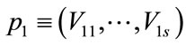
Circuits and Systems
Vol.4 No.5(2013), Article ID:36865,15 pages DOI:10.4236/cs.2013.45054
Analogue and Mixed-Signal Production Test Speed-Up by Means of Fault List Compression
Department of Electrical and Computer Engineering, Técnico Lisboa, Portugal
Email: nuno.m.guerreiro@ist.utl.pt, marcelino.santos@ist.utl.pt, paulo.teixeira@ist.utl.pt
Copyright © 2013 Nuno Guerreiro et al. This is an open access article distributed under the Creative Commons Attribution License, which permits unrestricted use, distribution, and reproduction in any medium, provided the original work is properly cited.
Received July 8, 2013; revised August 8, 2013; accepted August 15, 2013
Keywords: Test; Fault Model; Fault Clustering; Fault Simulation; Fault Representativeness; Analog; Mixed-Signal Test
ABSTRACT
Accurate test effectiveness estimation for analogue and mixed-signal Systems on a Chip (SoCs) is currently prohibitive in the design environment. One of the factors that sky rockets fault simulation costs is the number of structural faults which need to be simulated at circuit-level. The purpose of this paper is to propose a novel fault list compression technique by defining a stratified fault list, build with a set of “representative” faults, one per stratum. Criteria to partition the fault list in strata, and to identify representative faults are presented and discussed. A fault representativeness metric is proposed, based on an error probability. The proposed methodology allows different tradeoffs between fault list compression and fault representation accuracy. These tradeoffs may be optimized for each test preparation phase. The fault representativeness vs. fault list compression tradeoff is evaluated with an industrial case study—a DC-DC (switched buck converter). Although the methodology is presented in this paper using a very simple fault model, it may be easily extended to be used with more elaborate fault models. The proposed technique is a significant contribution to make mixed-signal fault simulation cost-effective as part of the production test preparation.
1. Introduction
Digital testing is a mature field, where many efficient methodologies and tools exist for production test preparation. However, in the analog and mixed-signal (AMS) testing domain, although reasonable approaches have been developed, they typically can only be applied to very simple case study circuits. Still, computational costs are prohibitive for real SoCs that are produced nowadays. Hence, there is a huge gap between what is published by research groups and what industry really needs in terms of AMS testing. The problem can be stated as follows: how can we demonstrate to a customer that the proposed test of his (her) AMS IP core verifies it and ensures a zero defect level product? The trend of increasing complexity, performance and speed of AMS devices poses significant challenges for test from a test yield and cost standpoint [1]. AMS circuits account for 70% of SoC test cost and 45% of test-development time, even though AMS functionality makes up a small fraction of the chip complexity [2]. The reasons for this situation may be summarized as follows: 1) there are no practical fault models (structurally-oriented), consequently 2) there are no Automatic Test Pattern Generators for AMS circuits, and 3) Design For Test (DFT) and Built-in Self-Test (BIST) solutions for AMS devices are still purely custom [2]. While trying to understand the root causes for this we find that AMS fault simulation costs for structural faults are still very high and a methodology for test stimuli generation (TPG) that uncovers structural faults is not defined yet. Thus, there is a need to lower AMS test costs. Moreover, an additional challenge exists: AMS test is mainly functional test, not structural test. Hence, it is very difficult to accurately prove to a customer the test effectiveness of the production test, based on the functional test. Many approaches have been proposed to overcome these challenges. Supply current monitoring for a quiescent state is widely used for digital circuits testing (IDDQ testing) [3]. The obvious advantage of IDDQ testing is that it does not require access to inner nodes of the structure. However, analog circuit IDDQ testing is significantly more difficult [3]. Moreover, diagnostic resolution of IDDQ testing is poor. IDDQ is found suitable only for catastrophic faults as the power supply current may be distinguishable only when the fault causes a change of current larger than the expected parametric scattering [4].
As stated, AMS test is mainly functional test. Analog circuits have traditionally been tested for critical specifications like AC gain over a range of frequencies, commonmode rejection ratio or signal-to-noise ratio, due to the lack of simple structural fault models [5]. However, the costly (time and resources) nature of AMS test preparation has motivated research into structural testing for analog circuits [6]. Nevertheless, no widely accepted fault models exist in the analog domain. Moreover, there is no automated way of minimizing the number of faults required to uncover likely physical defects in the structure of the entire AMS circuit [2]. Thus, no proven alternative to functionaloriented analog testing exists and more research in this area is needed [7]. An efficient strategy to test complex circuits is needed and the most promising approach is the Holy Grail of AMS: structural test [2]. Still, some difficulties arise: 1) the AMS cell definition, in a similar way to logic gate definition (in digital test environment); 2) a validation methodology to prove that a functional-oriented AMS test can also uncover structural faults. Therefore, there is a real need to develop a methodology for AMS SoCs testing, providing a methodology and tools for test preparation in the design phase.
In [8] a Computer-Aided-Test platform was developed to evaluate the test techniques for analogue and mixedsignal circuits. However, its operation is based on a statistical circuit performance analysis that accounts for process deviations. This is a good approach in a sense that it is useful to compare and improve different test techniques, by calculating analogue test metrics under process deviations. However, the lengthy Monte Carlo simulations process makes it less appealing. In [1] the authors developed a Mixed-Mode Fault Simulation approach for the analog fault coverage analysis at transistor-level, examining the faulty behavior in a structural way, along with the use of Hardware Description Language (HDL) models to perform the simulation in a manageable time. This approach is capable of uncovering structural faults, but the fact that it uses HDL models in some parts of the circuit reduces test accuracy that may not be tolerable, like in automotive applications.
In [9] a statistical approach is proposed for analog circuits under process variations. A hierarchical variability analysis for analog testing is performed, where both parametric and catastrophic faults are studied. A detectability metrics, based on the statistical distribution of each specification, is used to determine the best measurement sets that detect each fault. The circuit fault coverage (FC) is computed by summing all the detectabilities weighted by the occurrence probability of each fault. The test selection algorithm used results in appreciable reductions in the test time. In [10] the authors present an adaptive test strategy that adjusts the test sequence in order to cope with the properties of each individual instance of a circuit. It uses an initial test sequence ordering in order to boost the performance of the adaptive test elimination method. Test dropping is obtained by adapting the likelihoods of the unmeasured specifications passing the test, using the ongoing measurement results and a correlation matrix. This adaptive technique uses less resources with well-performing circuits, by passing them quickly, whereas more test time is used to test marginal devices (which do not fall near the nominal of the distribution space). An improvement in the test quality is obtained, for the same test time, with respect to other techniques.
In [11] the authors used a current measurement technique in order to improve the circuits fault coverage. This improvement is achieved by adding current measurements to the original specification based test program already present in the Defect Oriented Testing (DOT). An adaptive test strategy for the same DOT technique is presented in [12]. The test is prepared using a fast analog simulation algorithm Fault Sensitivity Analysis (FSA) that obtains the detection status of catastrophic faults in a manageable time. The proposed framework guides an optimized test selection, using a Greedy algorithm that eliminates redundant functional tests. This technique showed a defect simulation speed-up between 100 and 500 times for a specific design, when compared with the estimated standard simulation time. Moreover, by using more tightened specification limits, the defect coverage was improved. In [13] the authors explored the concept of fault equivalence in AMS circuits, by substantially reducing the number of structural faults that needed to be simulated. However, fault “equivalence” can be defined only in the particular case when anaccurate fault representation (one fault representing others) is possible and a more general representation concept can be defined that allows to truly explore the tradeoff between accuracy of representation and fault list compression.
In this paper, a completely different methodology is proposed, as a first step to overcome the limitations pointed above. We suggest a novel fault list compression technique for AMS cells, allowing cost-effective AMS low-level fault simulation. The proposed approach uses structural test along with stratified fault grouping, leading to the identification of a reduced set of “representative” faults. The estimated value for fault coverage may then be used to evaluate the test quality and to appropriately drive DFT efforts [14]. This technique was introduced in [15] but it was limited to single output cells (voltage signals). Now we extend its applicability to multiple output cells (voltage and/or current signals). An improvement in the selection of the test stimuli is also proposed to improve the fault compression rate for the same accuracy. The compressed structural fault list will be used to ascertain whether (or not) the production test is able to detect the structural faults (described at transistor level); if not, the designer may complement the production test set.
The paper is organized as follows: in Section 2, the new fault list compression technique is presented; an industrial DC-DC converter is studied in Section 3, where the fault compression technique is applied to the constituting blocks; Section 4 shows a fault representativeness evaluation for all the blocks in the DC-DC converter, that contain cells identified by our tool, as well as an improvement in the test quality of the DC-DC converter that contains two instances of a differential pair cell (DIFFpair); in Section 5 some conclusions are drawn.
2. Fault List Compression Technique
For digital circuits, structural testing has provided costefficient solutions that lead to high defects coverage, without functional test [8]. However, AMS testing significantly differs from digital testing. The major difference comes from the need to consider continuous signals and parametric deviations, in addition to just catastrophic faults (opens and shorts) [16]. In digital test, the impact of all internal physical defects at ate level is modeled by Boolean faults at input/output (I/O) nodes, e.g., using the single Line Stuck-At (LSA0, LSA1) fault model. Fault equivalence and collapsing are used to reduce the fault list. As only two voltage levels are relevant (VDD, VSS), gate-level fault simulation can be performed. When a test vector activates a fault, a complementary, erroneous Boolean value occurs at the cell’s I/O.
In analog test, analog cells can be identified, as they are extensively used (e.g., a differential pair, a common source amplifier, etc.). As a first step towards the search of representative faults, the analog cells, with basic functionality and appropriate granularity must be identified.
It is a well-known fact that non-catastrophic faults can also impact the performance and reliability of digital circuits. As a consequence, the traditional Line stuck-at fault model, used for the generation of a structural and static test, needs to be complemented with a performance evaluation test, which aims the detection of dynamic faults. Accordingly, in AMS circuits, a structural test that aims the detection of catastrophic/hard faults can be complemented by functional tests that evaluate the required performance. The proposed methodology aims the detection of hard faults and comprises five main steps that are explained bellow. Next, the methodology is applied to a DC-DC converter case study.
2.1. Analog Cell Definition
An initial question that arises when defining the analog cell boundaries refers to current mirror transistors. Shall these MOSFETs be included in a current mirror cell, or individually in each cell that uses a transistor as current source? A first analysis of a two stage comparator, with one current mirror transistor biasing the differential pair and another transistor of the same current mirror biasing the following common source stage, shows that a masking effect occurs for some faults that affect the current in both current mirror transistors. This masking effect has a parallel in the well-known difficulty found in the detection of faults in reconvergent fanout paths in digital circuits. Therefore, in the proposed technique, current mirror transistors are embedded in the analog cells they serve and no current mirror is defined as a primitive cell, except if it has a unique output current (when no masking effect is possible).
In digital circuits fault representativeness is obtained through fault equivalence and collapsing, analyzed at gate level. The granularity of a digital gate corresponds to the minimum functional block that can be analyzed at logic level with defined output values for all the possible input combinations. Faults are equivalent if, for all the possible input combinations, their impact on the output is the same.
Similarly, fault representativeness in analog circuits can be searched for the minimum size cells where functionality can be identified. Faults are grouped taking into account the similitude of their impact on the functionality when considering exhaustive input stimuli.
2.2. Structural Fault Model Selection
Faults should be defined in such a way that their detection allows the identification of permanent physical structure damage, due to a manufacturing defect (e.g., an open via). The structural test process will, thus, check the physical integrity of the manufactured IP core. In digital test, the LSA fault model, used to ensure the controllability and observability of the whole structure, is based on a static analysis. Parametric faults, not being properly modeled by the LSA model, need alternative test methods (like IDDQ or dynamic tests). Similarly, the proposed fault model aims at analyzing the structure integrity; therefore it is also based on catastrophic/hard faults. As in the digital test domain, the detection of some parametric faults is only possible using complementary test methods (e.g., functional test). In CMOS technology, cell branches are mainly composed of MOSFETs. Hence, the selected structural fault model is transistor stuck-on (TSON) (zero parallel resistance) and transistor stuck-off (TSOFF) (modeled by a 1012 Ω series resistance). For an analogue cell with t MOSFETs, the fault list will contain (f = 2t) faults.
2.3. Cell Fault Simulation (FS)
In order to evaluate the cell functionality in the presence of each fault, a set of stimuli capable of fully exercise the cell must be defined. Two approaches were evaluated for the stimulus definition:
● Operation-aware test: for the Fault-Free (FF) circuit and for all the faulty circuits (in each one, a single fault, Fi, is injected), all combinations of MOSFET regions of operation are identified (off, sub-threshold, triode, saturation). For each such combination, a test stimulus is generated. The test set will comprise s test stimuli. Some of the stimuli impose values unrealistic in the normal cell operation. For example, the DIFFpair cell, with a differential input voltage range [−2, 2] V, requires s = 87 stimuli.
● Sweep test: equally spaced test vectors, in the input range interval used in the cell normal functionality, are used. For the same DIFF pair cell, s = 33 stimuli are used for the input range [−340, 340] mV. This second approach proved to lead to the identification of better representative faults, by better exercising the cell functionality, as will be shown in the next sections.
Once the test set for cell fault simulation is defined, the values of the output variable (s) under observation (e.g., vO (t)) for each test stimulus and each simulation run (associated with the FF and single fault injection) are stored. Those values are combined to obtain several points, pi, in Rs, each point corresponding to one circuit response, obtained during a simulation run. Hence, the total set of vOi (t) values range from
 , (1)
, (1)
to
 (2)
(2)
where
 (3)
(3)
2.4. Fault Stratification
With the data collected in the cell FS step, we need criteria to cluster the structural faults in strata, according to their resemblance, in terms of similar responses. The proposed criterion is based on the computation of the faulty and FF circuit responses distances. An optimization algorithm is used to obtain the minimum for the sum of distances between every pair of representative and represented fault responses. These distances have been computed for different definitions (Euclidean distance, Manhattan distance, etc.). Attending to the definition of the Minkowski distance of order p,
 (4)
(4)
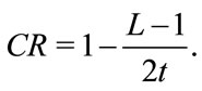
the Manhattan and the Euclidean distances correspond to the first and second orders, respectively. The Manhattan distance has been selected as the one leading to more accurate results. The number of strata, L, is used to define the trade-off between accuracy and FS effort. For L = 2t, each stratum contains only one fault, i.e., there will be no fault list compression. For L < 2t, one fault per stratum is selected to represent the other faults. Each stratum will thus contain one Representative Fault (RF), and a number of represented faults (which can even be zero). One of the strata will cluster faults whose responses are very close to the FF response. Hence, there will be no need to fault simulate for this stratum. Therefore, the number of faults in the reduced fault set will be (L − 1). The compression rate (CR) is
 (5)
(5)
Ultimately, the number of fault strata, L, will be user’s defined, allowing to choose the desired accuracy for each test preparation phase. Criteria for this choice are provided by the proposed methodology. Increasing L will increase fault representativeness; however, it decreases the compression rate. Figure 1 shows a stratification example where faults that originate responses p5, p6 and p10 are the RF; the other faults are the represented faults, being this combination of fault results the one that minimizes (for L = 3) the sum of the distances, d.
2.5. Error Evaluation
One degree of freedom is L, the number of representative faults that are chosen, and it may vary between one and the total number of faults (L = 1, 2, ..., f). This section explains how the error probability achieved by using L strata is computed. By selecting L < 2t, fault representation will occur with an error, which probability must be evaluated. When comparing the FS results, if the detection (or not detection, ND) status of a represented fault coincide with the one of its representative fault, no error occurs. However, if they differ (e.g., the RF is detected,

Figure 1. Fault stratification example: Three RF and seven represented faults in a universe of ten faults. Each faulty response, pi, contains two values (s = 2).
but the represented one is ND), the representation process introduced an error, which is the price paid to constrain the FS cost. Since the use of RF may introduce errors, more important than knowing the probability of one error it is important to quantify the probability of occurrence of n or more errors. In the proposed methodology, a metric for error evaluation is introduced, as follows:
Definition: En is the probability of occurrence of n or more errors. En is computed as a function of L in order to quantify the error probability for different compression ratios.
To obtain the data to calculate the error probability, again a set of test stimuli for error estimation must be generated, and the corresponding simulations must be performed. The number of test stimuli is similar to s, the number of test stimuli used in the analog cell FS. To compute this error probability, we consider that the circuit connected at the output of the analog cell under analysis has an unknown threshold value that is used to decide if each fault is detected or not. Therefore, for each applied stimulus, there is an error if the output given the presence of the representative fault is higher/lower than the threshold value whereas the output given the presence of the represented fault is lower/higher than the threshold value. To quantify the error probability, obtained by representing the 2t faults by L - 1 RF, the following method is proposed: First, the output value range is partitioned in k equal intervals that we refer as bins. Hence, a total of k + 1 possible output value levels are obtained (Figure 2). Then, for each stimulus, the corresponding output values for one pair of (representative and represented) faults are approximated to the nearest levels.
Finally, there is an error if the threshold value lies between those two levels. In this situation one fault is regarded as detected and the other one as not detected, thus, an error occurs. In the example shown on Figure 2, bins
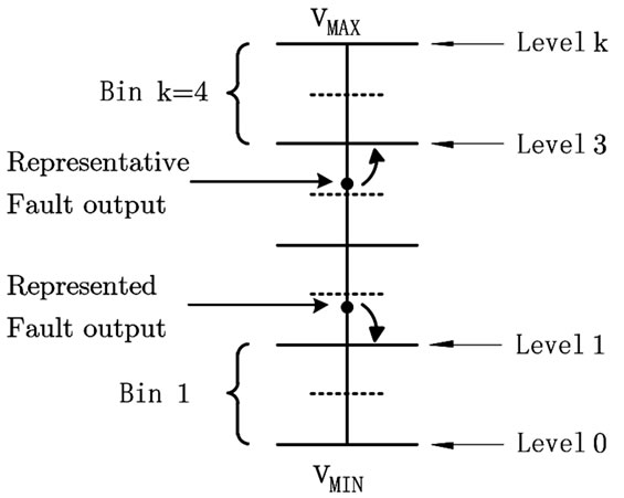
Figure 2. Example where the representative fault and the represented fault output values are quantized to the nearest levels (3 and 1), respectively.
2 and 3 contain one error each, since the RF output is approximated to level 3 and the represented fault output is approximated to level 1. It means that there may be an error if the unknown threshold value is found on bins 2 or 3; therefore, the number of errors is incremented on those bins. This evaluation is performed for every stimulus applied to the circuit in the presence of every pair of representative and corresponding represented faults and the errors obtained for the corresponding bins are summed. That is, the number of times each stimulus causes an error on each bin is counted and a table is created with this information. Table 1 is an example of such a table obtained using 4 bins and 5 input stimuli.
A second table is built by finding the number of errors in the previous table that are higher than or equal to n, for each stimulus and bin. Table 2 shows the entries where the number of errors is larger than or equal to n = 2, that are set to 1; the other entries are set to 0.
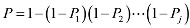
Taking the data of the second table, we sum the number of cases where the number of errors is higher than or equal to n. Dividing that value by the number of stimuli, s, multiplied by the number of bins, k, we get the error probability
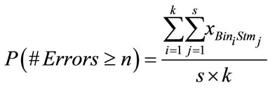 (6)
(6)
where
 (7)
(7)
that is obtained for a specific number of strata, L. A value of L is user’s defined, taking into account the fault list compression rate and the error probability, computed

Table 1. Number of errors example, obtained on each bin by the corresponding stimuli (Stm), when k = 4 and s = 5.
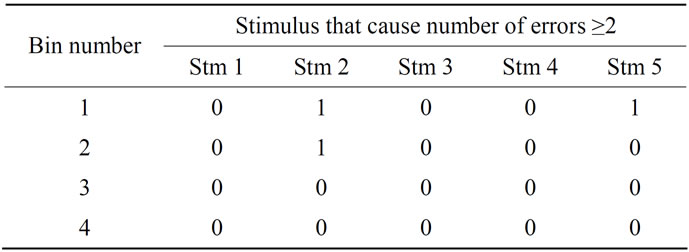
Table 2. Bins where the number of errors caused by a stimulus is higher than or equal to n = 2.
for each number of strata. In the analyzed case-study, a value of k = 300 was used. This number of bins was found to be appropriate for the analysis since smaller values lead to substantially different error probabilities and above this value the results don’t change significantly. Performing this analysis, for each integer value of L, the above mentioned probability is computed. Results show that even with low L values it is possible to obtain low probability values of 2 or more error occurrences, which shows that a significant fault list compression is possible without prohibitive sacrifice of FS accuracy.
3. DC-DC Converter Case Study
This research was driven by the need to reduce fault simulation effort in a real DC-DC converter industrial design. Therefore, priority was given to the identification of analog cells present in this case study. The DC-DC converter, implemented using a Chartered 65 nm CMOS technology, is composed of many blocks that are studied in this section. It contains two comparators that use one instance of a differential pair cell, each. The differential pair cell is one of the cells that is detailed in this section in order to illustrate the proposed methodology, while considering voltages as the input and output variables. Another relevant block is a current generator that contains several cells. It is studied to show how to apply the methodology while using multiple outputs and currents as output variables. A table that contains the statistics for the main blocks of the DC-DC converter is shown in the next section.
3.1. Differential Pair Cell Fault Stratification
The differential pair cell is composed of 7 transistors and is shown in Figure 3. For this cell, the exhaustive test, used for stratified fault grouping, can be obtained by exciting the inputs (VIP, VIN) with stimuli that drive the differential pair either into each possible combination of transistor states (Operation-aware test) or by applying equally spaced test vectors (Sweep test), as stated before. The testbench used for the research of potentially representative faults in the differential pair uses a common mode voltage source (CM) of 1 V and two signal sources
( ), as shown in Figure 4.
The differential pair is supplied with VDD = 2 V and different stimuli (VID = VIP − VIN) are applied at the inputs. For the Operation-aware test, Fault-Free and faulty simulation results for the 14 faults (7 transistor stuck-on, 7 stuck-off) are shown in Table 3, where only 5 of the total stimuli are shown.
Applying the method described in Subsection 2.4 to the differential pair cell and using the data partially presented in Table 3, distinct number of strata, L, where
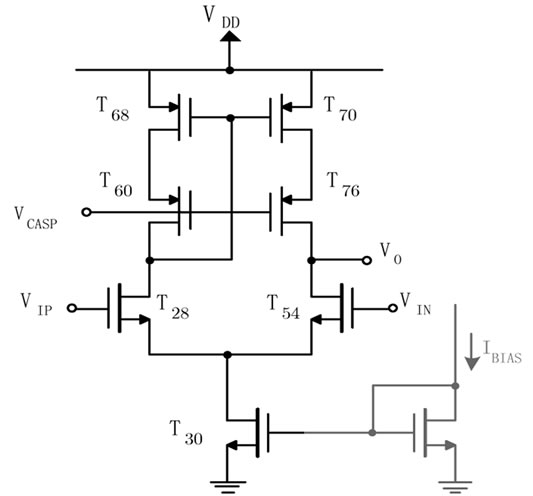
Figure 3. Differential pair cell schematic.

Figure 4. Differential pair cell test bench.
used. For every value of L in the set {1, ..., f}, the probability of occurrence of n or more errors was computed and it is presented in Figure 5, obtained for the set of 33 input stimuli that drive the MOSFET transistors to all possible operating zones (Operation-aware test), but taking the results given by stimuli in the range from −335 to 335 mV. The applied input voltage range was found appropriate to fully exercise the differential pair functionality, since for each limit the drained current shifts almost completely from one branch of the differential pair to the other. Each curve corresponds to one value of n. The curve that displays the highest probabilities corresponds to n = 1 (the probability of occurrence of one or more errors for each value of L). As expected, the error probability decreases when the number of strata and RF increases, allowing to exploit the tradeoff between accuracy and FS effort. For example, by using L = 3 (and simulating only L-1 = 2 RF) the probability of occurrence of more than n = 2 errors in this cell is reduced to almost zero.

Table 3. Differential pair output voltage, VO, for several differential input voltages, VID, in the presence of faults and for the fault free circuit.
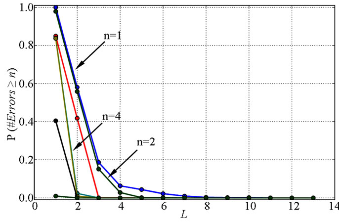
Figure 5. Diff. pair cell: Probability of error obtained with the exhaustive test set (33 input stimuli, driving the transistors to all possible state combinations for an input voltage in the interval [−335, 335] mV). The number of errors, n, varies from 1 to 8.
A similar result was obtained using the same procedure, but now with the (Sweep test), applying stimuli obtained by dividing the differential pair input voltage range in 100 equal steps and using only stimuli obtained from −340 to 340 mV. A total of 17 stimuli were used in this case. Table 4 shows the clusters of representative and represented faults for 3 strata (L = 3), where the RF are bold typed. Fault xt30-TSOFF is one that drives the cell output node to a high impedance state. Thus, this fault was removed from the fault representation analysis, since the resulting unpredictable behavior cannot be represented by any other fault results, so it is not present in the above mentioned table.
Figure 6 shows the error probability obtained using now the (Operation-aware test) but for the full input range [−2, 2] V. The results show higher probabilities than the ones obtained with a smaller range. This may be explained by the fact that the strata obtained in this case are not optimized for the operating zone of the differential pair (normally small differential input voltages). In the DC-DC converter under study, the differential pairs are excited with differential input voltages not greater than 300 mV. So, for this cell it is appropriate to use a small range for the input voltage, in order to select fault representatives that minimize the error probability.
Temperature, power supply voltage and process variations were applied to the DIFFpair cell, in the Fault stratification and Error evaluation steps (Sections 2.4 and 2.5). The clusters obtained were the same as the ones obtained without variations and little variations were observed in the error probabilities, for this cell. A more elaborate study is needed, in order to get an accurate measurement of this dependencies, which is not within the scope of this paper. Nevertheless, the results show limited impact of temperature, power supply voltage and process variations on the error probability.
3.2. Current Generator Cells Fault Stratification
The current generator is a block that contains one BiasLink cell, two CascodeBias cells and one IbiasSet cell, as shown in Figure 7. The analysis of the cells present in this block is done by applying variations to the nominal input current variable, IBIAS, performing a Sweep test for a range of ±30% around the nominal value. The output

Table 4. Representative and Represented Faults in the Differential Pair Cell for L = 3.
variables are the currents at the output nodes (IOUTiP and IOUTiN), for a total of 19 outputs. In this case the stratification step was performed using the k-means algorithm, as the number of output variables was quite large.
The error probability values computed for each output, obtained in the manner described in subsection 2.5, are combined to obtain the final error probability as follows:
 (9)
(9)
where Pi (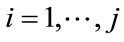 ), are the error probabilities obtained for the individual outputs.
As an illustration, Figure 8 shows the error probabilities obtained for the IbiasSet cell while considering only 5 output variables. The Sweep test was applied in a range of ±30% around the IBIAS nominal value, for a total of 20 input stimuli (s = 20). The results obtained for the total number of outputs on this block of the DC-DC converter are presented in the following section, where it was possible to get an optimal number of strata L = 39, for a total number of 76 faults from 19 outputs. The results obtained for the BiasLink cell and for the CascodeBias cells are also presented in the next section.
4. DC-DC Converter Fault Representativeness
The evaluation of the proposed fault representation technique is mandatory in order to ascertain if the exercised functionality and the accepted output difference leads to clusters of faults that are not detected or simultaneously detected when real circuits are submitted to production test. The testability analysis of a low complexity DC-DC converter industrial design, whose simplified block diagram is shown in Figure 9, requires circuit-level simulation of 1608 × 2 faults, taking 33 days!
The proposed technique aims at reducing the computational effort with limited impact on the accuracy of the obtained testability measure. To ascertain this, the fault simulation dictionary of the complete fault list was used, followed by a scenario of fault representativeness evaluation: for each individual fault in a stratum, the coincidence in the test strobe, that is, the coincidence in the
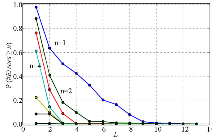
Figure 6. Diff. pair cell: Probability of error obtained with the exhaustive test set (87 input stimuli, driving the transistors to all possible state combinations for an input voltage in the interval [−2, 2] V). The number of errors, n, varies from 1 to 8.
observation instant is evaluated. The analog simulator used at Silicongate is hspice. Hence, the hspice netlist was used for cell recognition and fault injection, adding resistors where faults need to be injected. Analog fault simulation is carried out also with the hspice simulator. Fault injection is done by assigning an appropriate value to each resistor using. alter sections. Measures in specified simulation instants are the test strobes that allow fault dropping. Additionally, a timeout for the simulation of each fault is also used in order to limit computational effort. This fault simulation method was used to simulate all the faults in the DC-DC that already included Test Point Insertion (TPI) as design for testability solution. The test stimuli and measures used in the fault simulation process are the same as Silicongate provides in the product’s Test Integration Guidelines as being appropriate for production test. Different test modes are used, changing the DC-DC normal control actions. Each test mode drives the DC-DC into a state that allows the evaluation of specific static and/or dynamic behavior of selected nodes, made observable through an embedded analog multiplexer used for the TPI. Figure 9 shows the output signal used for test proposes (anatestbus), provided by the Analog Multiplexer block.
The testbench used in the design of all production test modes was used for the fault simulation of all the faults in de DC-DC. The fault simulation of 1608 × 2 faults during 33 days allowed the creation of a partial fault dictionary (only the first detection was registered). With the aim of being able to reduce the fault list size in the future, taking advantage of the proposed representative faults, a software tool was designed to recognize the basic cells. This cell recognition tool allowed the identification of the number of topologies present in the DC-DC listed in Table 5.
It can be concluded that a significant number of tran-
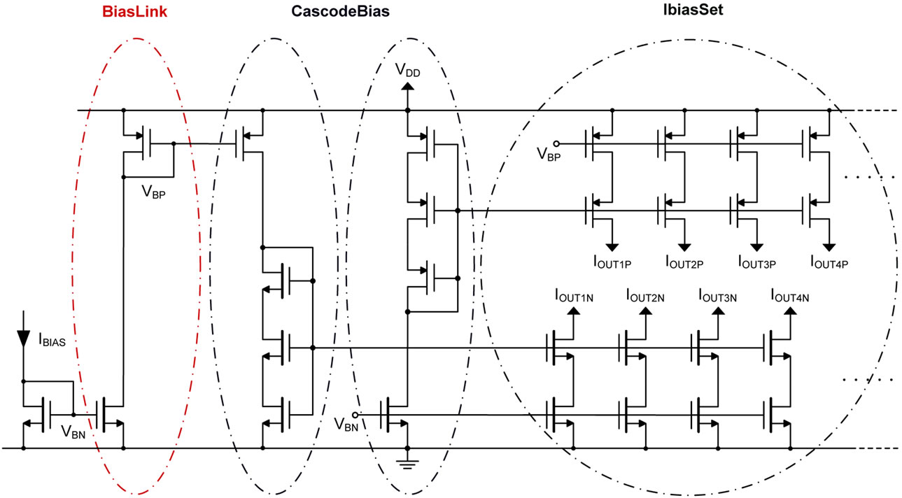
Figure 7. Current source generator simplified schematic where four cells are identified: One BiaLink Cell, two cascodeBias Cells and one IbiasSet Cell with multiple outputs.
Figure 8. IbiasSet Cell: Error probability obtained with the exhaustive test set (20 input stimuli for the Sweep test) in a range of ±30% around the IBIAS nominal value and for 5 output variables.
sistors is identified, remaining around 1/8 as unidentified. The tool has a graphical interface that details the statistics presented in Table 5 for each module of the circuit hierarchy. This interface helps identifying the modules where more unidentified transistors remain.
4.1. Differential Pair Fault Representativeness Evaluation
Fault simulation was carried out, by injecting only TSON and TSOFF faults in the two differential pairs of the DC-DC converter, either by injecting all the 28 listed faults (full fault list simulation), or by injecting only the 4 representative faults. Table 6 contains the results of the analysis of the exact measure that detects each fault in each stratum in each differential pair (D.P.1 and 2). The groups of representative and represented faults are the ones previously presented in Table 4, obtained for a number of representative faults L = 3. The group of faults present on Stratum 1 (undetectable faults) were not detected (ND) on both differential pairs. On Stratum 2 every fault was detected by Measures 13 and 1 on differential pairs 1 and 2, respectively. Stratum 3 contains faults that were not detected on D.P. 1 and were all detected by Measure 5 on D.P. 2. This evaluation confirms that, for two instances of the differential pair cell, all the faults are well represented by their representatives. Choosing this specific number of strata (L = 3), faults in each group were detected by a unique measure or were not detected.
The fault stratification procedure was carried out for every possible number of representatives (L), in the DIFFpair cell, and an evaluation was performed for both instances of this cell present in the DC-DC converter. Results are shown in Figure 10, where the used input stimuli correspond to the test associated with the referred “Measure”. In this figure, R represents the ratio of well represented faults in a stratum, that is, faults that lead to the same simulation result as the corresponding RF, i.e., when both the RF and the represented fault are simultaneously ND, or detected by the same Measure. The ratios of well represented faults, as a function of the number of strata, L, are shown for D.P. 1 and 2. The data in Figure 10 result from similar stratification of the faults using the same procedure, but two different sets of input stimuli
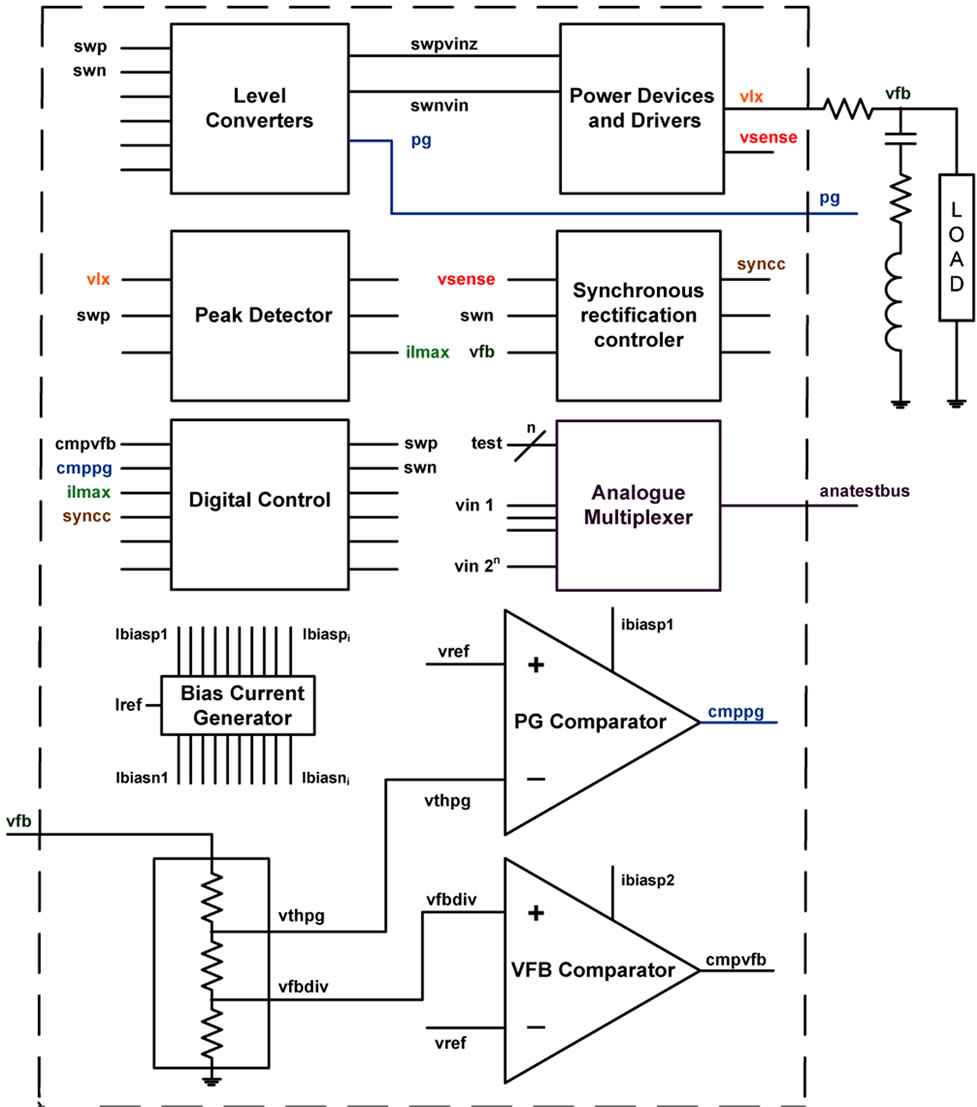
Figure 9. DC-DC converter block diagram in a production test environment.
(Operation-aware test or Sweep test). For the same number of strata, L, the same partition of the total population occurs when the 33 or the 17 input stimuli have been used; only the representative faults are different for some values of L, not affecting significantly the error probability results. The input set corresponding to the Operationaware test set (33 stimuli) leads to the same fault representativeness as the sweep set (17 stimuli): for L > 2, all faults are well represented on both differential pairs (Figure 10). The stimuli used to calculate the error probabilities were obtained in the same interval used for fault stratification, from −340 to 340 mV, shifted one unit, in order not to coincide with the ones used for the Sweep test set, as to avoid biasing the results.
4.2. DC-DC Converter Blocks Fault Representativeness Using the software tool referred above to identify all the seven cell types already processed by the methodology in the DC-DC converter and the complete fault dictionary, two tables were obtained. Table 7 presents the representativeness process evaluation. This is done for different levels of accuracy (Li) in the stratification process of all the cells in the various blocks by calculating the corresponding ratio of well represented faults (Ri). The three different levels of accuracy (L1 = Lmax, L2 = Lmed and L3 = Lmin) were analyzed taking into account the error probabilities obtained for each cell, that obey to the conditions shown in (9). Each of these levels of accuracy can be useful in different test preparation stages.
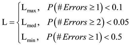
Table 5 presented before, contains the fault compression rate, calculated for every cell already processed by the methodology, using the referred different levels of accuracy shown in (9). This illustrates the trade-off between simulation effort and compression rate, for every cell, that is used for different phases of the test prepara
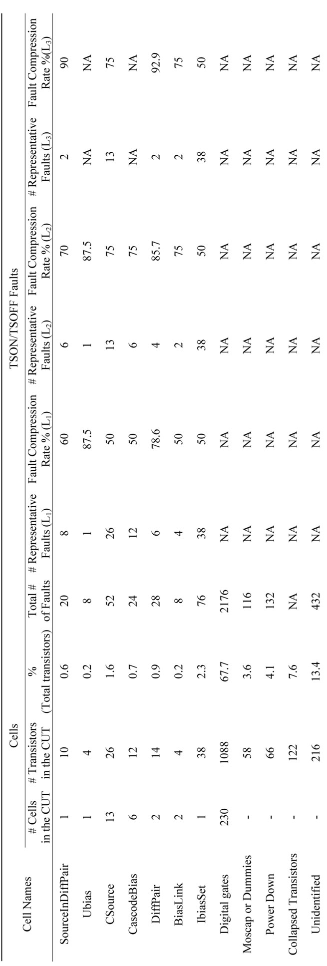
Table 5. Mixed-Signal Cells and Faults Identified in the DC-DC Converter, number of representative faults and compression rate for 3 different levels of accuracy (Li).

Figure 10. DC-DC Converter: Ratio between the faults that are well represented and all the faults in the differential pair instances, for RFs obtained with 32 stimuli that correspond to the transistor state combinations, in the input range [−340, 340] mV.
tion.
Table 8 contains the number of identified cells, number of faults per type of element and fault coverage (for the entire block and only for the identified cells on the block). It contains the estimated fault coverage and cells fault representation level (ratio of well represented faults in the cells) for three different levels of accuracy Li. Part of the peakdetector block schematics is presented in appendix A, showing two identified cell instances.
Taking the data on Table 8, the ratio of well represented faults in the cells already identified in the entire DC-DC converter was calculated for the 3 different levels of accuracy. A simulation effort reduction is obtained, as a consequence of the fault compression. Figure 11 represents the ratio of well represented faults as a function of the simulation effort, for the 3 different levels of accuracy considered. For the lowest level of accuracy, representing 86% of well represented faults in the entire circuit, we have a considerable simulation effort reduction, that is, an effort lower than 40%. For 97% of well represented faults we still have a quite low simulation effort, which is 56%.
4.3. Structural Fault Coverage Improvement
Observing Table 6 it is possible to conclude that the structural fault coverage obtained for the differential pair 2 (D.P. 2) is 100%, since all the detectable faults (on stratum 2 and 3) are detected by the production test used. This instance of the differential pair cell is part of the (VFB Comparator) found on the DC-DC converter partially represented in Figure 9. The other comparator (PG Comparator) contains D.P. 1 instance, for which the fault coverage is less than 100%, as 6 of the faults are not detected. This result shows that the test quality of the test set used may be improved. To increase the fault coverage

Table 6. Representative Faults evaluation without xt30- TSOFF Fault (L = 3).
an additional test stimulus and an additional Measure were designed to detect the undetected set of faults on D.P.1. Looking at Figure 9 we observe that the output signal of PG Comparator is connected to the Digital Control block input. This block has two output signals (swp, swn) that are connected to the Level Convertes block, whose outputs (swpvinz, swnvin) are in turn connected to the Power Devices and Drivers block. This last block delivers power to the load. The load voltage (vout = vfb) is sensed and is used to control the DC-DC operation, acting on both comparators in a feedback loop. Another signal present at the Level Converters block output is pg, that corresponds to the PG Comparator output signal (cmppg) after passing through the Digital Control block and the Level Converters block. This signal is made observable as a circuit output for system integration proposes, signaling whether the DC-DC is delivering the requested power or not, and may be used to test the differential pair (D.P. 1). This is possible because the PG Comparator output drives pg signal to logic level "1" when one of the faults on the second stratum of the inner differential pair is activated. Since this state (pg = “1”) corresponds to the transference of the requested power, to test the (D.P. 1) it is sufficient to force the control to drive the pg signal to logical level “0”, using an extra load to sink more current, and observe that this signal is kept permanently at logic level “1”, using an extra Measure. This improvement in the test set was implemented and it was possible to achieve 100% fault coverage for both differential pairs, simulating only 4 faults instead of 28.
5. Conclusion
In this paper, a method for reducing the fault simulation effort by simulating only representative faults (RF) is proposed for AMS circuits. The fault list compression technique includes analog cell identification, criteria for fault clustering in strata, according to a user’s defined number of strata, L, and RF identification. A trade-off between fault simulation effort and accuracy can be de

Table 7. Representativeness evaluation for sets of cells belonging to the same type, in the DC-DC converter, for different levels of accuracy (Li).
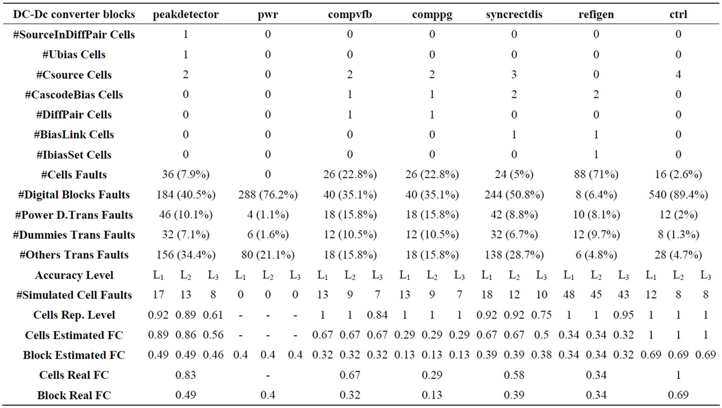
Table 8. DC-DC converter main blocks and corresponding statistics: number of identified cells, number of faults per type of element and Fault Coverage (for the entire block and only for the identified cells on the block) as well as Estimated Fault Coverage and Cells Representation Level for different levels of accuracy (Li).
fined for each test preparation phase: a fast, initial fault simulation can be performed with lower accuracy, just aiming to highlight testability problems. Then, later on, higher accuracy fault simulation can be used for the validation of the final test sequence. In order to support the selection of the appropriate number of RFs for each test preparation phase, a method is proposed for the evaluation of the probability of occurrence of n or more errors due to the RF-only simulation, and the assumption that the represented faults behave accordingly. The method was illustrated in a differential pair cell showing that using L = 3 (and simulating only L-1 = 2 RF) was enough to reduce to almost zero the probability of occurrence of more than n = 2 errors in 14 faults. The fault compression technique is further used in a commercial DC-DC converter that has two instances of this differential pair. Fault simulation results show that RF-only simulation does not lead to any error if L > 2, when the RFs are selected using an exhaustive test, going through all the combinations of the MOS regions of operation in the fault free and each faulty circuit or by applying equally spaced input stimuli in a narrow interval around the origin. The technique was then used in the main blocks of the DC-DC converter in order to show the quality of the representativeness process when applied to the seven types of cells identified. The impact of different levels of accuracy on the estimated fault coverage and representation level on each block was shown. Finally, a plot that shows the variation of the ratio of well represented faults as a function of the simulation effort of

Figure 11. DC-DC Converter: Ratio between the faults that are well represented and all the faults in the instances of the cells identified in the DC-DC converter.
the complete DC-DC converter was presented. The definition of the optimum stimuli for RF selection is now under research. More analog cells are being defined. Moreover, a preliminary analysis shows limited impact of temperature, power supply voltage and process variations on the error probability, which confirms the methodology reliability. The study of these dependencies is being carried out and it will be reported in the future.
6. Acknowledgements
This work was supported by national funds through FCT Fundação para a Ciência e a Tecnologia, under projects PEst-OE/EEI/LA0021/2013 and PTDC/EEA-ELC/1225 05/2010 and the PhD research grant SFRH/BD/61833/ 2009. The authors thank SiliconGate for providing the facilities and the case study that made this work possible.
REFERENCES
- J. Parky, S. Madhavapeddiz, A. Paglieri, C. Barrz and J. Abraham, “Defect-Based Analog Fault Coverage Analysis Using Mixed-Mode Fault Simulation,” IEEE 15th International of Mixed-Signals, Sensors and Systems Test Workshop, IMS3TW 09, Scottsdale, 10-12 June 2009, pp. 1-6.
- R. Wilson, “Under the Lid: Analog Test Is Suddenly the Critical Ingredient,” EDN, 7 January 2010. http://www.edn.com/electronics-news/4312835/Under-the-Lid-Analog-test-is-suddenly-the-critical-ingredient
- T. Golonek, D. Grzechca and J. Rutkowski, “Analog Ic Fault Diagnosis by Means of Supply Current Monitoring in Test Points Selected Evolutionarily,” International Conference on Signals and Electronic Systems (ICSES), Gliwice, 7-10 September 2010, pp. 397-400.
- S. Sindia, V. Singh and V. Agrawal, “Parametric Fault Diagnosis of Nonlinear Analog Circuits Using Polynomial Coefficients,” 23rd International Conference on VLSI Design, Bangalore, 3-7 January 2010, pp. 288-293.
- A. Madian, H. Amer and A. Eldesouky, “Catastrophic Short and Open Fault Detection in Mos Current Mode Circuits: A Case Study,” 12th Electronics Conference on Biennial Baltic (BEC), Tallinn, 4-6 October 2010, pp. 145-148.
- S. Spinks, C. Chalk, I. Bell and M. Zwolinski, “Generation and Verification of Tests for Analogue Circuits Subject to Process Parameter Deviations,” Proceedings of 1997 IEEE International Symposium on Defect and Fault Tolerance in VLSI Systems, Paris, 20-22 October 1997, pp. 100- 108.
- “International Technology Roadmap for Semiconductors,” 2009. http://www.itrs.net/Links/2009ITRS/2009Chapters_2009Tables/2009_ExecSum.pdf
- A. Bounceur, S. Mir and E. Simeu, “Cat Platform for Analogue and Mixed-Signal Test Evaluation and Optimization,” International Conference in Very Large Scale Integration, Nice, 16-18 October 2006, pp. 320-325. doi:10.1109/VLSISOC.2006.313254
- F. Lui and S. Ozev, “Statistical Test Development for Analog Circuits under High Process Variations,” IEEE Transactions on Computer-Aided Design of Integrated Circuits and Systems, Vol. 26, No. 8, 2007, pp. 1465- 1477.
- E. Yilmaz and S. Ozev, “Test Application for Analog/rf Circuits with Low Computational Burden,” IEEE Transactions on Computer-Aided Design of Integrated Circuits and Systems, Vol. 31, No. 6, 2012, pp. 968-979.
- L. Fang, Y. Zhong, H. van Donk and Y. Xing, “Implementation of Defect Oriented Testing and ICCQ Testing for Industrial Mixed-Signal IC,” 16th Asian Test Symposium, Biejing, 8-11 October 2007, pp. 404-412. doi:10.1109/ATS.2007.93
- B. Kruseman, B. Tasic, C. Hora, J. Dohmen, H. Hashempour, M. van Beurden and Y. Xing, “Defect Oriented Testing for Analog/Mixed-Signal Designs,” IEEE Design & Test of Computers, Vol. 29, No. 5, 2012, pp. 72-80. doi:10.1109/MDT.2012.2210852
- N. Guerreiro and M. Santos, “Mixed-Signal Fault Equivalence: Search and Evaluation,” 20th Asian Test Symposium (ATS), New Delhi, 20-23 November 2011, pp. 377- 382.
- M. L. Bushnell and V. D. Agrawal, “Essentials of Electronic Testing for Digital, Memory and Mixed-Signal VLSI Circuits,” Kluwer Academic Publishers, city, 2002.
- N. Guerreiro, M. Santos and P. Teixeira, “Fault List Compression for Cost-Effective Analogue and Mixed-Signal Fault Simulation,” 27thConference on Design of Circuits and Integrated Systems, Avignon, 28-30 November 2012, pp. 261-266.
- A. Bounceur, S. Mir and E. Simeu, “Estimation of Test Metrics for the Optimisation of Analogue Circuit Testing,” Journal of Electronic Testing, Vol. 23, No. 6, 2007, pp. 471-484. doi:10.1007/s10836-007-5006-6
Appendix
Other DC-DC Converter Block Cells
This schematic contains part of the peakdetector block where two cell instances are shown, namely, Ubias and SourceInDiffPair (see Figure 12).
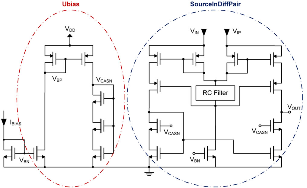
Figure 12. DC-DC Converter: Source input comparator and polarization circuit. Two identified cells: Ubias and SourceInDiffPair.