Journal of Modern Physics
Vol.3 No.7(2012), Article ID:21089,4 pages DOI:10.4236/jmp.2012.37073
Elaboration and Characterization of AuCl Semiconductor Nanocrystals Embedded in KCl Single Crystals
1Laboratoire d’Etude des Matériaux (LEM), Département de Physique, Facultés des Sciences Exactes et des Sciences de la Nature et de la Vie, Université de Jijel, Wilaya de Jijel, Algeria
2Laboratoire de Cristallographie (LC), Université de Mentouri-Constantine, Wilaya de Constantine, Algeria
Email: *zehanifouzia@yahoo.fr
Received April 10, 2012; revised May 11, 2012; accepted June 8, 2012
Keywords: AuCl; Semiconductor nanocrystals; X-ray diffraction; Photoluminescence
ABSTRACT
In this work, we investigated the structural and the optical properties of AuCl semiconductor nanocrystals embedded in KCl single crystals. The AuCl nanocrystals were obtained by doping the KCl crystalline matrix with gold using the Czochralski method. The X-ray diffraction showed the formation of the AuCl nanocrystals in KCl with a tetragonal structure. The average radius of the AuCl nanocrystals is estimated using the Scherrer formula. The photoluminescence spectra presented a band emission situated at 580 nm leading to the formation of the AuCl nanocrystals within KCl.
1. Introduction
Semiconductor nanocrystals embedded in wide gap matrices, such as alkali halides [1,2] have in recent years a great interest for both fundamental research and technical application. From the technological point of view, the main motivation for studying nanocrystals is to search new applications by controlling their physical properties as a function of size [3]. The nanocrystals are characterized by a dominant surface effect and they have a considerable surface/volume [4]. In that respect, the optical properties of semiconductor considerably change when their sizes become comparable to the bulk Bohr radius of exciton [3]. This change permits to get the quantum confinement of the electronic excitations [5]. The confinement in three dimensions of the exciton could be at the origin of strong nonlinear properties, which make them suitable materials for use in laser devices.
Gold(I) chloride (AuCl) belong to the family of elements I-VII having semiconductor properties, was the subject of little studies. The optical properties of AuCl were studied by Claude Schwab et al. [6] and T. N. Silukova et al. [7]. They showed that the luminescence of the gold monochloride has a narrow band and a broad band situated respectively at 472.2 nm (2.62 eV) and 632 nm (1.96 eV). But their crystallographic properties were studied by E. M. W. Janssen et al. They found that the AuCl has a body-centered tetragonal structure with a space group I41/amd [8].
The aim of this work is to elaborate and study the structural and the optical properties of AuCl nanocrystals embedded in a KCl crystalline lattice; which is a dielectric material and transparent in the visible range. It is the range of optical response of AuCl nanocrystals. The characterization of AuCl nanocrystals in KCl has been studied by using the X-ray diffraction and the photoluminescence (PL).
2. Experimental
The samples of KCl single crystals doped AuCl nanocrystals are elaborated using the Czochralski method, which consists of melting the gold thin films deposited on pure KCl pastilles. The growth process is performed by using a seed oriented [100]. The obtained single crystals have cylindrical shape and transparent colour. The single crystals are cleaved perpendicularly to the crystallographic direction [100]. The cleavage permits to obtain samples with 1 mm thickness. The thermal treatment of samples is performed at 650˚C during 3 hours. After the annealing, the samples are cooled slowly at room temperature.
The crystalline structure was analysed with X-ray diffraction (XRD) by a Bruker D8 advanced diffractometer system with Cu irradiation (λkα = 1.54056 Å) at 40 kV and 40 mA in the 2θ range (10˚ - 80˚). The photoluminescence (PL) spectra were measured with a Jobin-Yvon spectrofluorometer Fluorolog-3 using a Xenon lamp (450 W).
3. Results and Discussion
3.1. X-Ray Diffraction
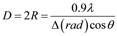
Figure 1 exhibits the X-ray diffraction of pure KCl samples. We observe two very intense peaks situated at 2θ = 28.37˚ and 2θ = 58.68˚, corresponding to (200) plane and its harmonic (400) of KCl single crystals, as identified by using JCPDS file 41-1476.
X-ray diffraction of KCl doped AuCl nanocrystals after annealing at 650˚C for 3 h, is showed in Figure 2. The spectrum shows the intense peaks of KCl single crystals and two diffraction peaks with a weak intensity, situated at 2θ = 31.74˚ and 2θ = 65.83˚. These peaks are attributed respectively to (211) and (422) planes of AuCl tetragonal structure with a space group I41/amd, comparing with the literature data of JCPDS file 30-0603. We note that the AuCl presents a preferential orientation along (211) and (422) planes, because of the oriented growth of KCl single crystals obtainedby the Czochralski method. We observe that the (400) peak of KCl is very intense that (200) comparing with those of spectrum of pure KCl. This change may be due to doping of the KCl matrix by the AuCl.
A slight shift of the AuCl peak angular positions towards higher angles can be noticed in comparison to the standard position indicated in the JCPDS file 30-0603. This shift may be attributed to the contraction of the AuCl nanocrystals cells in KCl lattice [9].
Therefore, X-ray diffraction results confirm the formation and the embedding of AuCl nanocrystals in KCl matrix.
We assume that the shape of AuCl nanocrystal embedded in KCl was spherical. The average radiuses (R) of AuCl were estimated using Scherer’s formula [10]:
where:
D is the average diameter of the nanocrystals
λ is the wavelength of the X-ray radiation
θ is the Bragg angle diffraction
Δ is the full-width at half-maximum (FWHM) of the peak.
The average radius of AuCl nanocrystals in KCl corresponding to each diffracting plan is reported in Table 1. We note a large dispersion of AuCl nanocrystals size in KCl. It is varied between 3.4 and 18.7 nm.
3.2. Photoluminescence
PL spectra of pure KCl and KCl doped AuCl nanocrystals after annealing at 650˚C for 3 h and excited with λex
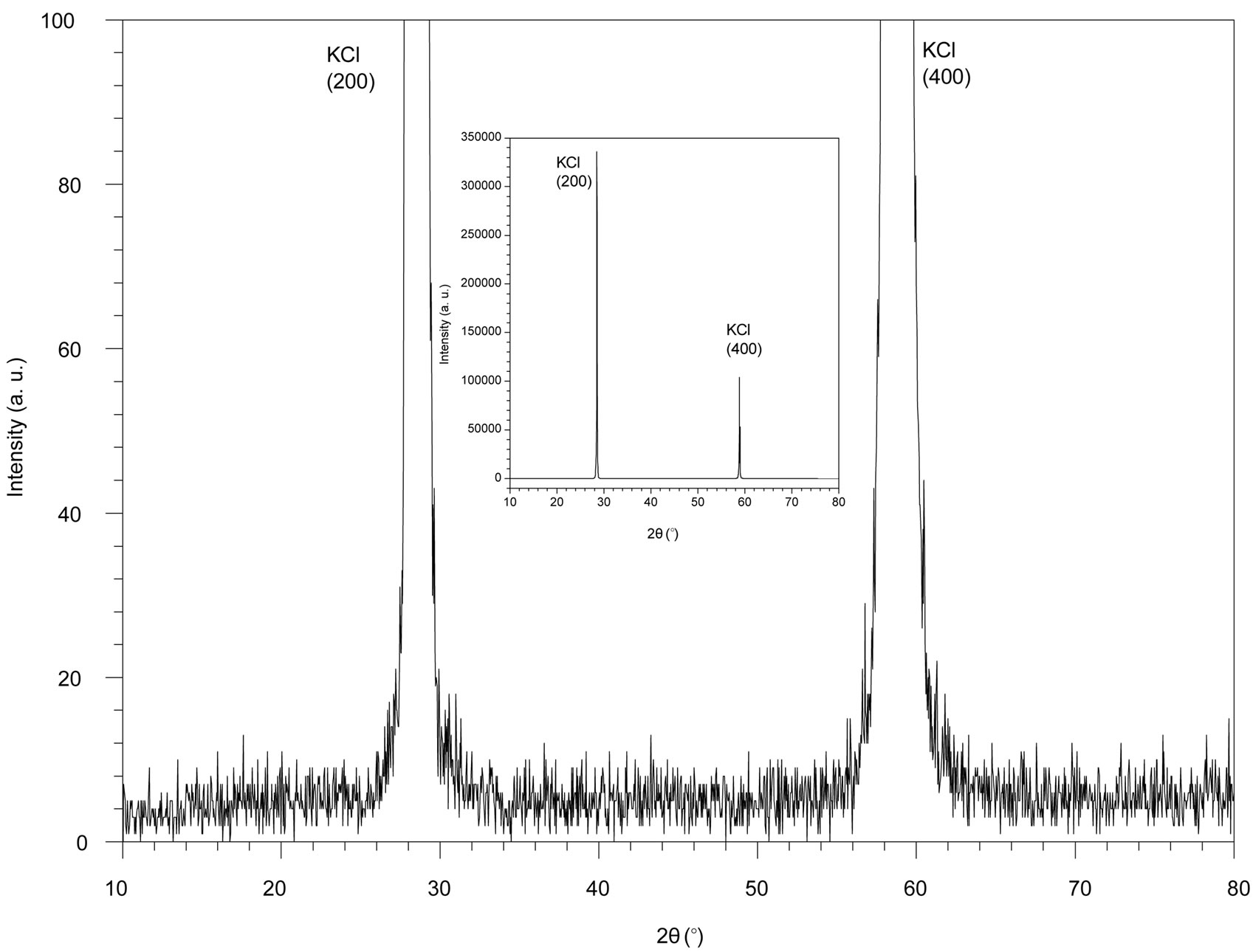
Figure 1. X-ray spectrum of pure KCl single crystals.
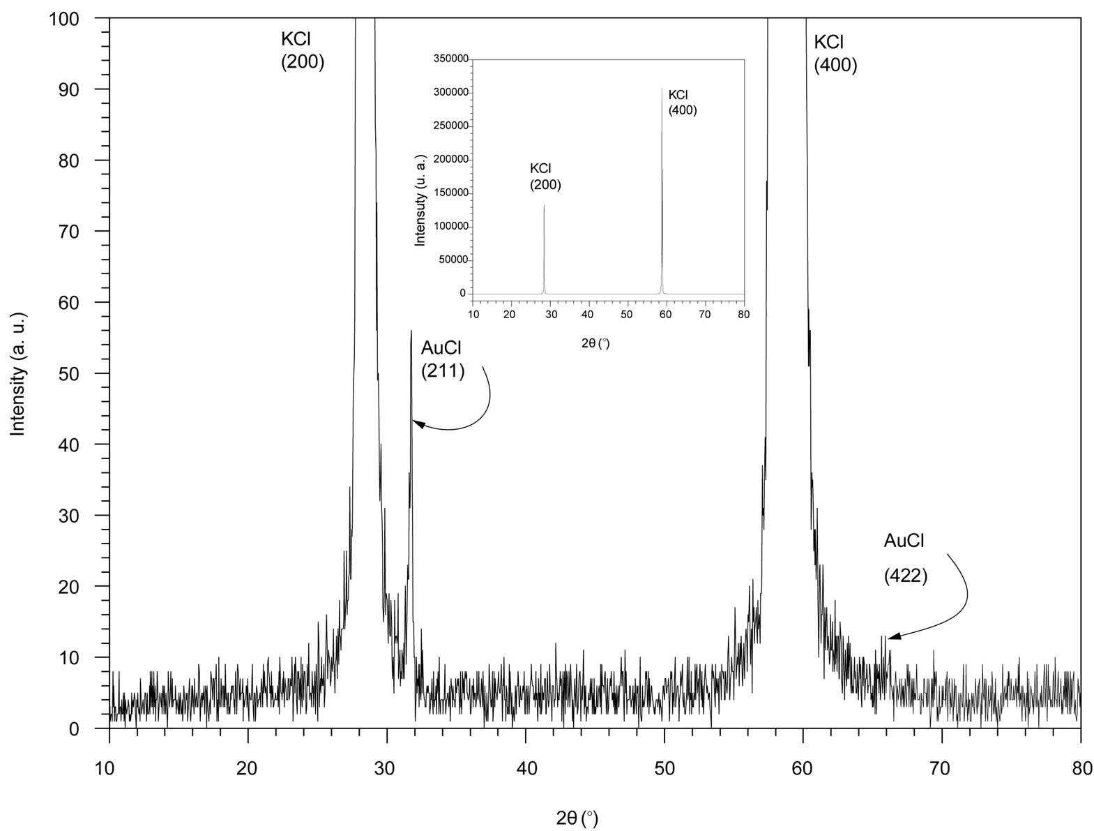
Figure 2. X-ray spectrum of KCl single crystals doped AuCl after annealing at 650˚C for 3 h.
= 300 nm at room temperature, are reported in Figure 3. Indeed, for the spectrum ofpure KCl single crystals (Figure 3(a)), noemission bandcould be detected. However, the spectrum of KCl doped AuCl (Figure 3(b))
Table 1. Nanocrystal sizes of AuCl calculated from XRD.
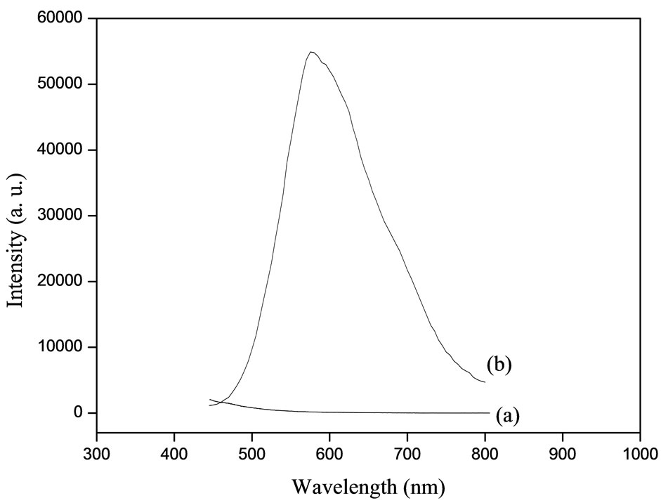
Figure 3. PL spectra (λex = 360 nm) of: (a) pure KCl and (b) KCl doped AuCl nanocrystals.
shows a emission band centered at 580 nm (2.14 eV). We assign this band to AuCl nanocrystals with a shift from the bulk equal 52 nm (0.18 eV) [6]. The enlargement of this band can be explained by the presence of size dispersion of AuCl nanocrystals inside KCl (Table 1).
4. Conclusion
KCl single crystals doped AuCl nanocrystals were prepared by the Czochralski method. Structural characterization by XRD shows the formation of AuCl nanocrystals in KCl with a tetragonal structure. However, the PL measurements exhibit the characteristic emission band of AuCl nanocrystals situated at 2.14 eV (0.18 eV shift from bulk of AuCl).
REFERENCES
- T. Itoh, Y. Iwabuch and M. Kotaoka, “Study on the Size and Shape of CuCl Microcrystals Embedded in AlkaliHalide Matrices and Their Correlation with Excitons Confinement,” Physica Status Solidi (b), Vol. 145, No. 2, 1988, pp. 567-577. doi:10.1002/pssb.2221450222
- T. Itoh, Y. Iwabuch and T. Kirihara, “Size-Quantized Excitons in Microcrystals of Cuprous Halides Embedded in Alkali-Halide Matrices,” Physica Status Solidi (b), Vol. 146, No. 2, 1988, pp. 531-543. doi:10.1002/pssb.2221460215
- A. I. Ekimov, “Optical Properties of Semiconductor Quantum Dots in Glass Matrix,” Physica Scripta, Vol. 1991, 1991, pp. 217-222. doi:10.1088/0031-8949/1991/T39/033
- A. Ekimov, “Growth and Optical Properties of Semiconductor Nanocrystals in a Gass Matrix,” Journal of Luminescence, Vol. 70, No. 1-6, 1996, pp. 1-20.
- A. I. Ekimov, A. L. Efros, M. G. Ivanov, A. A. Onushchenko and S. K. Shumilov, “Donor-Like Exciton in Zero-Dimension Semiconductor Structures,” Solid State Communications, Vol. 69, No. 5,1989, pp. 565-568. doi:10.1016/0038-1098(89)90242-1
- C. Schwab, et al., “Propriétés Optiques de AuCl aux Basses Temperatures,” Comptes Rendus de l’Académie des Sciences, 1967, pp. 1739-1742.
- T. N. Silukova, P. A. Babin, S. F. Voroparev and V. G. Plekhanov, “Luminescence of Excitons in Gold Monochloride,” Optics and Spectroscopy, Vol. 46, No. 2, 1979, pp. 218-219.
- E. M. W. Janssen, J. C. W. Folmer and G. A. Weigers, “The Preparation and Crystal Structure of Gold Monochloride, AuCl,” Journal of the Less Common Metals, Vol. 38, No. 1, 1974, pp. 71-76. doi:10.1016/0022-5088(74)90204-5
- M. Samah, H. Khelfane, M. Bouguerra, A. Chergui, M. A. Belkhir and S. Mahtout, “Optical Responses of AlkaliHalide Matrix (NaCl)-Doped Silver,” Physica E, Vol. 23, No. 1-2, 2004, pp. 217-220. doi:10.1016/j.physe.2004.03.009
- H. Benelmadjat, B. Boudine, O. Halimi and M. Sebais, “Fabrication and Characterization of Pure and Sn/SbDoped ZnO Thin Films Deposited by Sol-Gel Method,” Optics & Laser Technology, Vol. 41, No. 5, 2009, pp. 630-633. doi:10.1016/j.optlastec.2008.09.011
NOTES
*Corresponding author.