Journal of Modern Physics
Vol.3 No.5(2012), Article ID:19251,5 pages DOI:10.4236/jmp.2012.35053
In-Situ Study of Silicon Single Crystals Conductivity under Electron Irradiation
1A.I. Alikhanyan National Science Laboratory (YerPhI), Yerevan, Armenia
2Institute of Metrology Republic of Armenia, Yerevan, Armenia
3State Nuclear Safety Regulatory Committee by the Government of Armenia, Yerevan, Armenia
Email: *Grant@yerphi.am
Received February 23, 2012; revised March 12, 2012; accepted March 23, 2012
Keywords: Silicon; Radiation Defects (RD); Carrier Concentration; Carrier Mobility; Conductivity
ABSTRACT
The influence of electron radiation on the properties of semiconducting silicon single crystals (Si)—both nand p-types (currently one of the most widely applied material in the electronic technology) was studied under the electron irradiation process in-situ in air (in common conditions). Higher value of electro-conductivity (σ) during the irradiation process with respect to after irradiation was observed, which was explained by ionization and capture mechanisms resulting in the formation of non-equilibrium carriers (hole-electron pairs). The kinetics of radiation defects generation, their physical nature, temperature stability and relaxation are examined. Structural radiation defects formation: point and complexes, their influence on the silicon conductivity are considered.
1. Introduction
There are numerous investigations concerning the influence of irradiations on the properties of solid states (including silicon) which are carried out before and after irradiation [for example 1-14]. The works on studying the properties of solid states directly under the irradiation process are very scarce [15-20]. However, these works describe the situation in more adequate conditions and are important in terms of using silicon devices, for instance in space, nuclear plants, in particle accelerators. In present study silicon conductivity (the main property for practical usage) measurements are carried out directly under the electron irradiation process.
The nature of radiation structural defects depends on type, energy, dose and intensity of radiation [1,2,4]. The charged particles interact with atoms in the material by means of long-distance Coulomnic forces, resulting in frequent, but weak collisions. The neutral particles transfer large amount of energy to the atomic nucleus and the constituent atoms undergo infrequent, but energetic collisions. In the first process, the formation of large number of simple vacancy-interstitial type atoms predominates; while in the second case large disordered areas (clusters), consisting of hundreds, thousands of simple defects are formed. The difference in these mechanisms results in different properties of the radiated materials, and it is very difficult to specify common equivalents for radiation by charged particles or for radiation by neutral particles.
However, it is possible to find common features when comparing the effect of different charged particles on a particular material. For example, when modeling some effects in semiconductors it is reasonable to substitute protons and α-particles with energy of several МeV—by electrons with energies of tens MeV. Nevertheless, each type of radiation-substitution requires its own particular and detailed analysis, because even when both kinds of radiation consist of charged particles there is no absolute equivalence, because of different defect densities in the tracks of particles with different masses.
In this paper the results of in-situ measurements of specific conductivity of silicon single crystals (both nand p-type) under electron irradiation with energy 8 MeV in air (in common conditions) are presented.
2. Experimental Procedure
Both pand n-types of silicon samples with initial electro physical parameters (see Table 1) have the following sizes: thickness 0.4 mm; width 4 mm, length 10mm and distance between contacts 5 mm.
Conductivity, mobility and carrier concentration were measured by Hall Effect equipment having following parameters: magnetic field induction 0.3 Tesla; Hall-potential and contact differential voltage were measured by voltmeter B7-34A (Russian production) with input impedance of 2 × 10¹⁰ Ω and accuracy of 5%. The electrical parameters of the samples are given in Tables 1, 2.
The Ohmic contacts were made by Ga: Zn compound with relation 1:4. In-situ measurements were performed at the distance of 7 m from the exit window of the linear accelerator; the measuring test current through sample was 1 mA. Electron beam current from linear accelerator has pulse form with length 5 microsecond and frequency of 200 Hz. The electron irradiation current was indicated by the “Faraday cap” and irradiation dose was determined by D = It/S×6.25×1012 el/cm2, where I is mean current of the beam in μA, t—exposure time in seconds, S—cross section of the beam in cm2.
3. Results and Discussion
The measurements results of specific conductivity (σ) versus electron radiation dose for both n-Si:P and p-Si:B are presented in Figure 1. The electrical parameters of the samples, measured under the irradiation process for maximal irradiation dose of 4 × 10¹⁵ el/cm2 and after switch off irradiation beam are given in Table 1. As it is obvious from Figure 1 the dose dependence of logσ for both types of Si are of the same quality; there are two intervals of almost linear dependences of logσ versus logD (D-irradiation dose). However, for n-Si the inflection point (indicated by row) on the logσ (logD) curve is located at the 4 × 10¹⁴ el/cm2, while for p-Si this point is located at the 1.5 × 10¹⁵ el/cm2.
It is seen that the specific conductivity of Si-samples, measured at the irradiation process and after irradiationhas different values.
In order to elucidate the sharp decreasing of samples’ conductivity (up to degradation) after irradiation, a temperature dependence of the Hall Effect measurements were carried out from 285 K to 315 K. In Figures 2-4 the temperature dependencies of conductivity, mobility and concentration of main carriers are presented. The main feature is that the specific conductivity change rate is higher for n-Si than for p-Si.
These results can be explained as follows.
It is known, that the irradiation by electron with energy 8 MeV forms in Si crystals structural point and complex defects (in particular, with impurity), so called “secondary radiation defects” (SRD) [1-6]. At low irradiation doses mainly point defect production may occur, while at high doses SRD formation becomes preferable, and moreover, clusters are formed too [5].
Generally, the introduction of radiation defects (RD) leads to reduction of concentration of main carrier concentration and their mobility in crystal. The degree of variation of these parameters depends on the initial properties of the Si-samples, energy, dose and irradiation intensity. When RD clusters are formed, the corresponding centers are more efficient, and changes of parameters occur at lower doses. Energetic levels of RD in the forbidden gap of n-Si have been determined according to thermal dependence of carrier concentrations at different irradiation doses taking into account the capture probability of vacancies by matrix and non-matrix atoms. After irradiation by dose of 4 × 10¹⁵ el/cm2 the following activation energies of RD are calculated 0.395 eV; 0.53 eV in n-Si and 0.56 eV; 0.66 eV in p-Si which stimulate conductivity because the carriers’ mobility has a weak dose dependence. Among many known energetic levels in Si [1-15] corresponding to different RD, Figures 2-4 present energetic levels, which are identified to defined levels in literature. For example, the observed level of 0.395 eV can be classified as E-center with location on
Table 1. Electrical parameters of studied samples before irradiation.
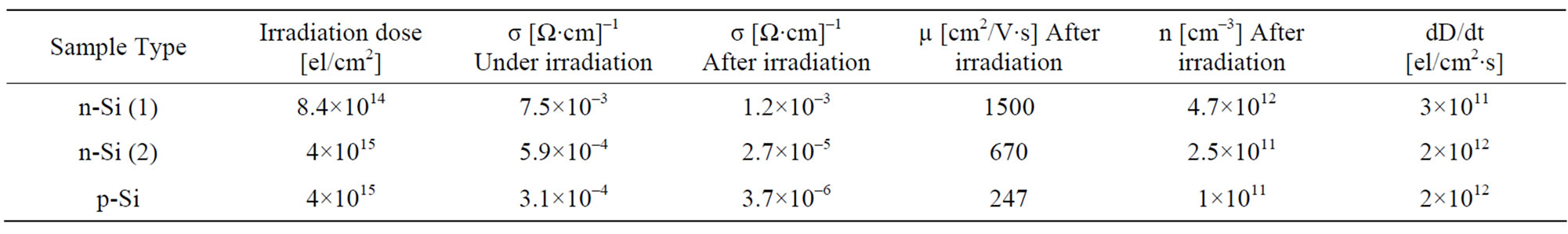
Table 2. Electrical parameters of studied samples after irradiation by electrons with energy 8 MeV and different intensity (dD/dt).
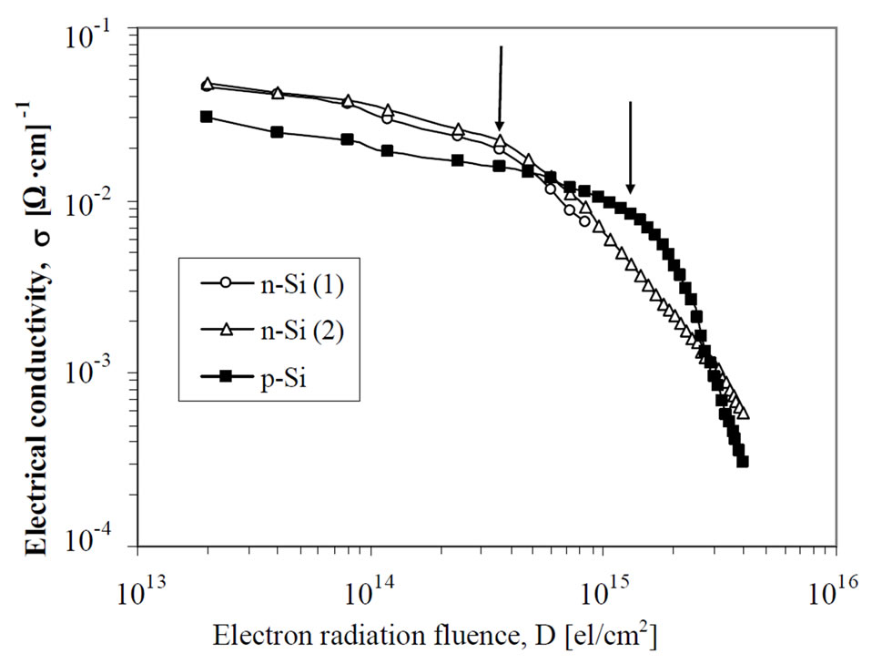
Figure 1. Specific conductivity of n-Si and p-Si versus electron radiation dose. The measurements were carried out insitu during electron radiation with energy of 8 MeV.
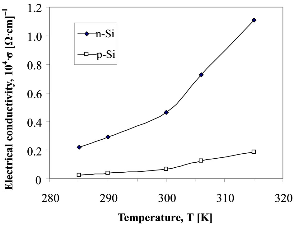
Figure 2. Temperature dependence of specific conductivity for nand p-types Si after radiation by electrons with energy 8 МеV and dose 4 × 10¹⁵ el/cm2.
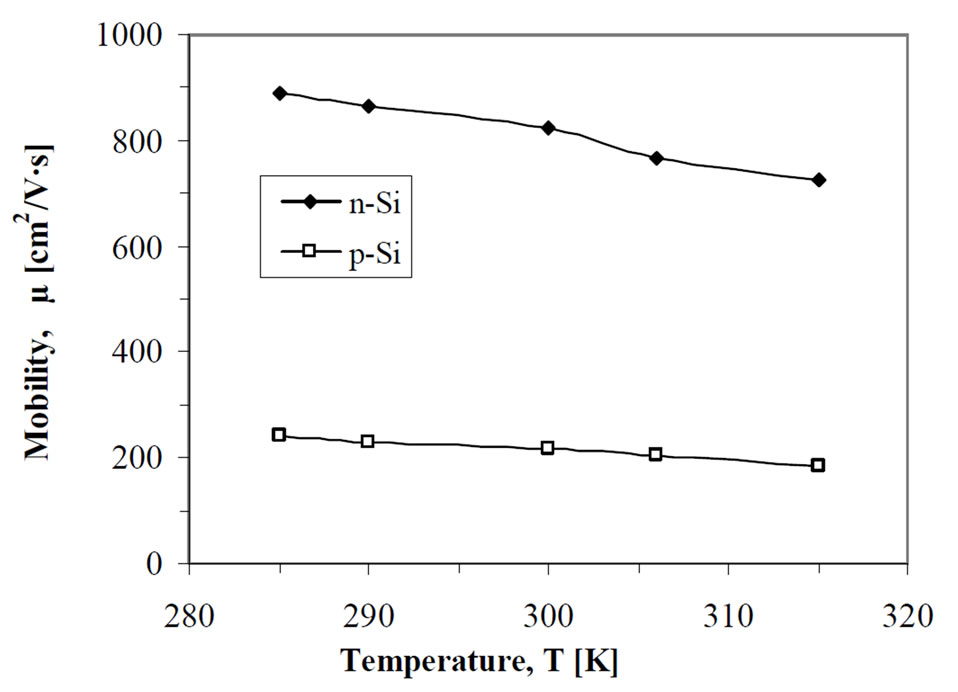
Figure 3. Temperature dependence of mobility of electrons and holes in nand pof types of silicon after irradiation by electrons with energy 8 МеV and dose 4 × 10¹⁵ el/cm2.
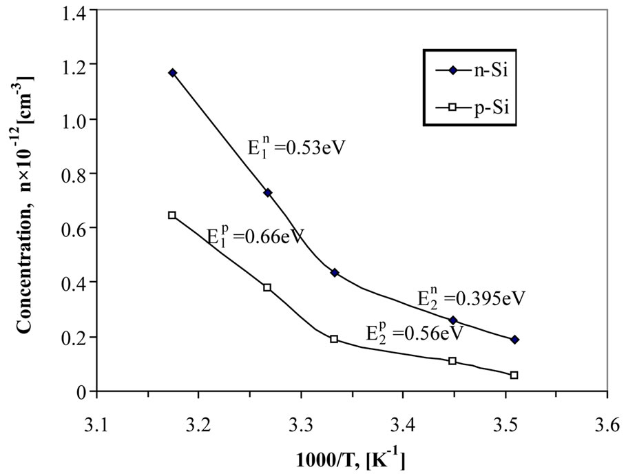
Figure 4. Dependence of electrons and holes concentrations versus reciprocal temperature in nand p-types of silicon after irradiation by electrons with energy 8 МеV and dose 4 × 10¹⁵ el/cm2. (En = 0. 47 eV; Ep = 0. 61 eV).
Ec 0.4 eV in the forbidden gap of Si [7-9,12,13], i.e. vacancy of Si atom + donor impurity atom, while the levels of 0.53 eV and 0.56 eV are near Ec 0.54 eV and Ec 0.55 eV which were identified as bi-vacancy. However, it was revealed that these levels coincide to bi-vacancy only on annealing temperature [11]. The observed level of 0.66 eV is near Ec 0.65 eV and was identified after electron irradiation of Si by electrons with energy 10 MeV [15].
Apart from known A-centres, (interstitial oxygen atom + Si-vacancy) and E-centres (donor atom + Si-vacancy), new centres with Ес 0.33 eV; Ес 0.40 eV and Ес 0.22 eV have been found and studied in literature [1-15]. The first one is connected with interstitial Si atom, the second one corresponds to bi-vacancy and the third one is identified as bi-vacancy + oxygen (C-centre) [1,3,7,8]. The appearance of last centre is explained by the fact that during irradiation process more vacancies are formed in samples at high fluencies and part of them can either connect with each other and be captured with oxygen atom, or form A-centre and then connect with other vacancy and form a complex C-centre [1,3,8,9,13].
When considering the mobility problem, two known mechanisms should be taken into account: scattering on the phonons at high temperatures and scattering on the ionized impurities at low temperatures. The irradiation mainly influences on the second mechanism, although the obtained data suggest that there might be other mechanisms that may explain the observed phenomena, for instance in А3В5 compounds. The mobility behavior quickly changes when irradiated by high energy or high dose and intensity: an anomalous in the temperature mobility occurs, i.e. in the law of μ~Tj, j may obtain values higher than known 3/2. This is stipulated by creation of disordered regions in crystals surrounded by spatial charge, which significantly increases the scattering of carriers [5,7,8]. The mobility of charge carriers depends on initial material, too. In samples with higher concentration of impurities, this anomalous phenomenon happens at higher doses of irradiation, than in samples with lower concentration of impurities. With the increase of irradiation dose (1016 - 1017 el/cm2), the temperature region of anomalous dependence shifts to higher temperatures.
Note, that mentioned defects are stable and they act as both scattering and capture centers, i.e. decreases carriers mobility and their concentration. The analysis shows (Table 2) that the concentration of carriers decreases rapidly (103 times) than the mobility (tenth percents), so one can conclude more important role of different capture properties of radiation defects which take place under irradiation and at post-irradiation processes.
4. Conclusions
Thus the results given above bring to following conclusions:
• Irradiation induces into Si different RD, concentration and character of which highly depends on sample temperature and also on dose of ionizing radiation. At high temperatures, the generated RDs are highly stable and their concentration depending on sample temperature, dose shows non-monotonous character. Efficiency of RD introduction into n-Si shows maxima with increase of electron beam dose.
• The higher value of σ under the irradiation process is due to ionization mechanisms (Auger or other irradiation induced process) which results in the formation of non-equilibrium carriers (hole-electron pairs). These carriers are accelerated in reverse directions by switching on electrical field which gives additional contribution to the specific conductivity. However, after switching-off the beam, part of non-equilibrium carriers migrate through the sample and occupy more stable defined charge states. At the same time the carriers generated by electron beam at non-equilibrium state are captured by the radiation centers (SRD clusters and so on) and not take part in conductivity, which is confirmed by formation of high concentration effective capturing radiation centers.
• The analysis show a formation of mainly deep centers with energetic levels Ec 0.395 eV; Ec 0.53 eV in n-Si and Ec 0.56 eV; Ec 0.66 eV in p-Si in the forbidden gap of the Si crystals which are responsible for decreasing and degradation of conductivity.
• This work demonstrates the importance of in-situ study of radiation defect production in solids which describes the results in real situation.
REFERENCES
- B. N. Mukashev, Kh. A. Abdullin and Yu. V. Gorelkinski, “Metastable and Bistable Defects Isilicon,” Uspekhi Fizicheskikh Nauk, Vol. 170, No. 2, 2000, pp. 143-154 (in Russian). doi:10.3367/UFNr.0170.200002b.0143
- C. Leroy and P.-G. Rancoita, “Particle Interaction and Displacement Damage in Silicon Devices Operated in Radiation Environments,” Reports on Progress in Physics, Vol. 70, No. 4, 2007, pp. 493-625. doi:10.1088/0034-4885/70/4/R01
- Sh. Makhkamov, N. A. Tursunov, M. Ashurov, R. P. Saidov and Z. M. Khakimov, “Formation of Radiation Defects in Silicon Structures under Low-Intensity Electron Irradiation,” Semiconductor Science and Technology, Vol. 16, No. 7, 2001, pp. 543-547. doi:10.1088/0268-1242/16/7/303
- L. I. Murin, V. P. Markevich, I. F. Medvedeva and L. Dobaczewski, “Bistability and Electrical Activity of the Vacancy-Dioxygen Defect in Silicon,” Fizika i Tekhnika Poluprovodnikov, Vol. 40, No. 11, 2006, pp. 1316-1320 (in Russian).
- T. A. Pagava, “A Study of Recombination Centers in an Irradiated p-Si,” Fizika i Tekhnika Poluprovodnikov, Vol. 38, No. 6, 2004, pp. 665-669 (in Russian).
- V. S. Vavilov, “Atomic Migration and Defect Concentration and Structure Changes Due to Electronic Subsystem Excitations in a Semiconductor,” Uspekhi Fizicheskikh Nauk, Vol. 167, No. 4, 1997, pp. 407-412 (in Russian). doi:10.3367/UFNr.0167.199704c.0407
- N. Yarykin and J. Weber, “Interaction of Copper Impurity with Radiation Defects in Boron-Doped Silicon,” Fizika i Tekhnika Poluprovodnikov, Vol. 44, No. 8, 2010, pp. 1017-1020 (in Russian).
- V. B. Molodkin, S. I. Olikhovskii, E. G. Len1, B. V. Sheludchenko1, et al., “X-Ray Diffraction Characterization of Microdefects in Silicon Crystals after High-Energy Electron Irradiation,” Physica Status Solidi (A), Vol. 208, No. 11, 2011, pp. 2552-2557. doi:10.1002/pssa.201184253
- V. S. Vavilov, “Origine and Energetic Specter of Radiation Damages in Semiconductors,” Uspekhi Fizicheskikh Nauk, Vol. 54, No. 3, 1964, pp. 431-450 (in Russian).
- V. V. Emtsev, A. M. Ivanov, V. V. Kozlovski, A. A. Lebedev, G. A. Oganesyan, N. B. Strokan and G. Wagner, “Similarities and Distinctions of Defect Production by Fast Electron and Proton Irradiation: Moderately Doped Silicon and Silicon Carbide of n-Type,” Fizika i Tekhnika Poluprovodnikov, Vol. 46, No. 4, 2012, pp. 473-481 (in Russian).
- T. A. Pagava, “Annealing Peculiarities for RadiationInduced Defects in p-Si Crystals,” Fizika i Tekhnika Poluprovodnikov, Vol. 41, No. 6, 2007, pp. 651-653 (in Russian).
- G.-F. Chen, W.-B. Yan, H.-J. Chen, H.-Y. Cui and Y.-X. Li, “Infrared Studies of Oxygen-Related Complexes in Electron-Irradiated Cz-Si,” Chinese Physics B, Vol. 18, No. 7, 2009, p. 2988.
- A. N. Gorban, V. V. Kravchina, D. M. Gomolskii and A. I. Solodovnik, “Features of Formation of Silicon Diodes Fast Recovery,” Technology and Fabrication of Electron Devices, Vol. 3, No. 3, 2008, pp. 36-40 (in Russian).
- K. D. Shcherbachev, V. T. Bublik, V. N. Mordkovich and D. M. Pazhin, “Features of Radiation Defects Formation in a Silicon Layer ‘Silicon on Insulator’ Structures,” Fizika i Tekhnika Poluprovodnikov, Vol. 45, No. 6, 2011, pp. 754-758 (in Russian).
- V. V. Lukyanitsa, “Determination of Energy Levels of Elementary Primary Defects in Silicon,” Fizika i Tekhnika Poluprovodnikov, Vol. 33, No. 8, 1999, pp. 921-923 (in Russian).
- M. Yu. Barabanenkov, A. V. Leonov, V. N. Mordkovich and N. M. Omelyanovskaya, “Effect of in Situ Photoexcitation of n-Type Si as a Result of Ion Implantation at Low Doses on the Formation of Radiation Defects,” Fizika i Tekhnika Poluprovodnikov, Vol. 33, No. 5, 1999, pp. 537-541 (in Russian).
- M. Yu. Barabanenkov, A. V. Leonov, V. N. Mordkovich and N. M. Omelyanovskaya, “Pecularities of Radiation Defect Formation under Photon Assisted Low Dose Ion Implantation of p-Si,” Fizika i Tekhnika Poluprovodnikov, Vol. 33, No. 8, 1999, pp. 897-899 (in Russian).
- Yu. I. Golovin, A. A. Dmitrievskiĭ and N. Yu. Suchkova, “Influence of the Type and Concentration of a Dopant on the Dynamics of the Beta-Induced Variation in the Microhardness of Silicon,” Physics of the Solid State, Vol. 50, No. 1, 2088, pp. 25-27.
- K. D. Shcherbachev, V. T. Bublik, V. N. Mordkovich and D. M. Pazhin, “The Effect of in Situ Photoexcitation on the Generation of Damaged Structures during Ion Implantation into Si Wafers,” Journal of Physics D: Applied Physics, Vol. 38, No. 10A, 2005, pp. A126-A131.
- P. C. Srivastava, O. P. Sinha, J. K. Tripathi and D. Kabiraj, “In Situ I-V Study of Swift (~100 MeV) O6+ Ion-Irradiated Pd/n-Si Devices,” Semiconductor Science and Technology, Vol. 17, No. 9, 2002, pp. L44-L46. doi:10.1088/0268-1242/17/9/102
NOTES
*Corresponding author.