World Journal of Condensed Matter Physics
Vol.07 No.01(2017), Article ID:74463,10 pages
10.4236/wjcmp.2017.71004
Nanometer Thick Diffused Hafnium and Titanium Oxide Light Sensing Film Structures
Fred J. Cadieu1,2, Lev Murokh1,2
1Department of Physics, Queens College of CUNY, Flushing, NY, USA
2Graduate Center of CUNY, New York, NY, USA

Copyright © 2017 by authors and Scientific Research Publishing Inc.
This work is licensed under the Creative Commons Attribution International License (CC BY 4.0).
http://creativecommons.org/licenses/by/4.0/


Received: January 8, 2017; Accepted: February 25, 2017; Published: February 28, 2017
ABSTRACT
We examine 10 nm thick film structures containing either Hf or Ti sandwiched between two respective oxide layers. The layers are deposited onto heated substrates to create a diffusion region. We observe a high degree of light sensitivity of the electric current through the film thickness for one polarity of an applied voltage. For the other polarity, the current is not affected by the light. We explain the observed phenomenology using the single- particle model based on the existence of interface states on the metal-oxide interfaces.
Keywords:
Thin Film, Light Sensing, Current Enhancement, Interface States, Hafnium, Titanium

A high degree of light sensitivity has been observed in certain hafnium dioxide and titanium dioxide diffused structures. This behavior is illustrated in Figure 1. Such light sensitive behavior is the subject of US Patent No. 9,040,982 Issue Date 05/26/2015, Inventor: Fred J. Cadieu [1] [2] . Certain thin oxide films of principally Ti and Hf have been important for non-light related applications. Recently hafnium oxide films in which the hafnium oxide exhibits an exceptionally high dielectric constant have proven enabling for the fabrication of 45 nm versus otherwise 65 nm linewidth semiconductor circuits [3] [4] [5] . Also of note is that new circuit elements called memristors have been made by using principally oxygen depleted Ti oxide nanostructures in which the electrical resistivity exhibits hysteresis characterized by bow-tie type pinched I versus V curves [6] . Similarly to the case of magnetic films that exhibit magnetic hysteresis, the “current state or resistance” of memristors depends upon whether the voltage is rising or falling allowing their use as compact memory elements [7] [8] . The interest in
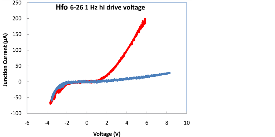
Figure 1. Current versus voltage curves are shown for a junction formed by the intersection of top and bottom conducting stripes. The relatively flat curve is the dark response. The curve dipping sharply up for positive bias values shows the response when exposed to white light.
the memristor type films was mainly for high density data storage so that the objective was to make patterned features with dimensions much less than the wavelengths of visible light. In contrast to that case, the effort here is to make junctions or pixels comparable or greater in size than the wavelengths of visible light. The elements Ti and Hf are in the same column of the periodic table and are expected to exhibit analogous physical and electrical properties. Titanium dioxide, dielectric constant 2.6, and hafnium dioxide, dielectric constant 25, can be made in degradations of oxygen depletion by sputtering the materials in different argon-oxygen mixtures at various substrate temperatures. In our studies, the use of Si device wafers as substrates has allowed a dual utility role in that the possible film devices can be directly exploited as a part of silicon device technology and the smoothness of Si device wafers allows a very powerful tool of x-ray reflectivity to be used for thickness and composition studies. The devices of the patent, Ref. 1, have been made by sputtering Hf sequentially in oxygen, then in argon, and then in oxygen again onto heated Si substrates. The length of sputtering time for the first oxide layer was about 3 times longer than the sputtering time for last oxide capping layer. The film layering of these devices has been analyzed by X-ray reflectivity. In order to fit the reflectivity data it is necessary to account for diffused oxygen depleted layer. The thicknesses of films sputtered in oxygen and argon under similar sputtering conditions were calibrated by X-Ray reflectivity measurements [10] . The combined thickness of the hafnium oxide, depleted oxide, and top oxide layer is 10 - 12 nanometer. The films exhibit a high lateral electrical resistance, and also a high resistance measured across the thickness of the film structure. The special feature of this film layer is that the through the film thickness electrical resistance can be changed by exposure to certain wavelengths of light and in the most general case for light across the entire visible and near infrared range of light wavelengths. The change in the electrical resistance also exhibits a diode type character in that the change in electrical resistance upon exposure to light only occurs when a bias voltage is applied in what is termed the positive direction. It should be noted that because the thin film structure exhibits a high lateral electrical resistance that it has not been necessary to pattern the thin film structure in any way to have each junction region act independent of any other junction region. The top and bottom conducting stripes used here are evaporated aluminum metallic stripes. But transparent conducting material such as graphene have also been demonstrated [1] .
As illustrated in Figure 2, samples with an array of 75 junctions have been deposited onto ≈ 25 mm x ≈ 60 mm silicon device substrates. The junctions have been labeled yj, xi where j can range from 1 to 5, and i from 1 to 15. To ensure that there is a high resistance between the y-stripes it is advisable to use either intrinsic silicon, or silicon that has been over coated with an oxide layer, or an over coat of intrinsic silicon. At the present time we have not been able to achieve uniform junction properties across an entire substrate. This illustrates that junction diode behavior and light response are very sensitive to deposition temperatures and times. For test purposes voltages from about −5 V to +5 V were applied across the junctions in series with a 5 kΩ to100 kΩ current sensing resistor one at a time. Figure 3 shows the light sensitive responses as measured at junction y2, x4 for a simple LED strobe flashlight. The data sampling rate was increased to 10 kHz to better follow the time response. The ratio of the light to dark current was about 48 times at 3 V for a saturating strobe light intensity. The increase in the electrical conductivity is roughly proportional to the illumination intensity up to some saturation value.
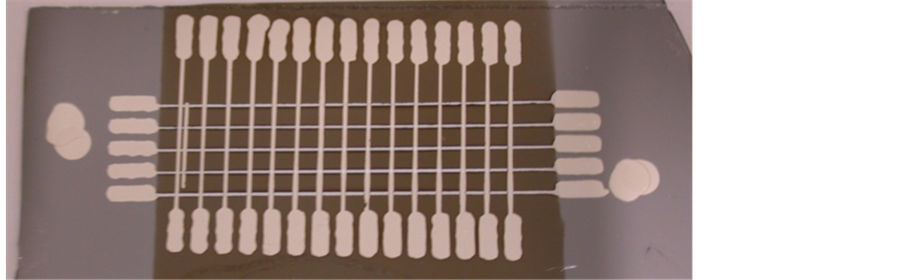
Figure 2. This picture shows a sample made onto a silicon substrate. The silicon surface shows as grey in the picture. Next aluminum conducting stripes y1, y2, …and y5 were evaporated onto the oxidized silicon surface. Next Hf was sputtered in oxygen, then in Ar, and then in oxygen again with the silicon surface heated to a temperature sufficiently high to cause diffusion to occur. The initial Hf in oxygen sputtering was for about 3 times as long as the final layer which acted to yield diode type current versus voltage behavior. The hafnium oxide diffused region shows as brown in the photograph and is mostly transparent since it has a total thickness of approximately 10 nm. Finally Al cross stripes x1, x2, x3, … x15 were evaporated.

Figure 3. The current through the film thickness for junction y1, x6 for the white light LED strobe light is shown for an applied voltages of 3 V across junction and 5 kΩ serial connected resistor for different strobe light intensities. The data sampling rate was 10 kHz. At saturation the light to dark current ratio was 48. Solid Red Line 500 Lumen strobe, Dashed Green Line 250 Lumen strobe, Long Dash Dot Line 150 Lumen strobe. Lumen numbers should be considered relative values only.
This research benefited from studies using various oxide films such as tantalum oxide, aluminum oxide, titanium oxide, and hafnium oxide films to constitute boundary adhesion layers to allow the deposition of strongly adherent metallic films onto Si semiconductor device wafers [11] . Ta, Al, Ti, Hf, and TaxO1-x, AlxO1-x, TixO1-x, HfxO1-x, films have been made by sputtering the respective element in either argon or oxygen onto heated Si device wafers. X-Ray reflectivity measurements were used to characterize the films and their respective deposition rates. The intensity modulation for hafnium dioxide films was up to two orders of magnitude and the largest for any of the metal oxide systems studied [10] .
An LED white strobe light was also used to illuminate a junction in open circuit configuration as shown in Figure 4 with leads just connected to a voltmeter. Without illumination, the voltage was zero, while when illuminated the top surface contact exhibited a voltage of −0.042 V.
Figure 5 shows the junction current as a function of time for 1 Hz square wave biasing voltage as the junction was illuminated with a white LED strobe light at a steady rate of approximately 10 Hz. It can be seen that there is a response to the strobe light only when the top surface is positive during the square wave bias voltage cycle. The 3 volt square wave bias was applied across the com- bination of the junction y4, x7 in this case in series with a 5 kΩ resistor. The actual junction resistance is always large compared to the 5 kΩ resistor. The ratio of the current during illumination compared to the dark current was approximately a factor of 20. The behavior illustrated here is consistent with that expected from Figure 1.

Figure 4. The voltage developed across a junction in open mode for the same white light LED strobe light is shown for a voltage sampling rate of 10 kHz. In the absence of light the voltage was zero while in the presence of light the top surface contact exhibited a voltage of −0.042 V.

Figure 5. The junction current for a 1Hz 3 V amplitude square wave bias with a con- tinuous ≈10 Hz strobe illumination is shown.
Since there are four connections to each junction region, it is possible to do four terminal measurements of each junction. Such behavior is shown in Figure 6 for a HfO type junction with the bias voltage scanned sinusoidal at 0.1 Hz while the white LED strobe light is flashing on and off at 10 Hz across the entire bias voltage range. Only for bias voltages greater than +0.6 volts is there any response to the flashing light. The apparent current oscillations are just due to the junction resistance responding to the light and switching from the lower curve to upper curve envelope in agreement with the expectations from Figure 1. The data sampling rate was 10 kHz.
Figure 7 shows the junction current for a film sample made using Ti in place of Hf. The respective layer sputtering times were inversely proportional to the sputtering rates for Ti compared to Hf. The thicknesses of the respective film layers in a sample made using Ti in place of Hf should then be the same. The current for an illuminated junction versus the dark current is a function of 7 in this case, but the overall behavior is very similar as for the Hf based samples. The conditions for the Ti based sample fabrications have not been optimized, nor is the light intensity believed to approach saturation in this case.
We believe that the enhancement of the current is caused by the presence of interface states. These states are located at the interface of the diffused oxygen depleted layer and the second HfO2 layer. Similar states are known to exist at the Si/SiO2 interfaces [13] [14] and caused by the oxygen dangling bonds or oxygen vacancies. Their energies are within the infrared frequency range from the conduction band of the oxygen-depleted layer in agreement with the 1 eV redshift of the luminescence of the porous silicon quantum dots which occur due to such
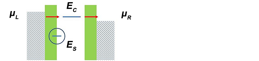
states [15] . These states are also known to affect drastically the transport characteristics of the junction of two different oxide layers [16] [17] . To explain the unidirectionality of the current enhancement, we employ the following simplified single-particle model. The electron states inside the HfO are modelled by a single-particle level with the energy EC, located in the conduction window between the chemical potential of the reservoirs, whereas the surface states are modelled as a single-particle level with the energy ES. This system is shown in Figure 8 for the case of no light illumination. When the voltage is applied, so the chemical potential of the left lead is larger than the chemical potential of the right lead, the particle current is directed from left to right, see Figure 8(a). In the opposite case, the particles are transferred from right to left, Figure 8(b). The surface states are always populated, because the level ES is always well below the chemical potentials and it is not involved in transport processes. It should be noted that the electron transfer is symmetrical, so the current-voltage characteristics should be symmetrical as well in the absence of light.
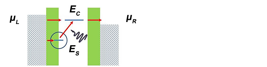
In the case of the light illumination, the electrons from the surface states can be elevated to the conduction band via the photon absorption. It would open the possibility for another transport channel in addition to the direct electron transfer from the left to the right. It is shown in Figure 9(a). After the absorption of aphoton, electrons are promoted to the EC level and can proceed to the right re-

Figure 6. Junction current versus voltage characteristics are shown for a HfO based structure with a sinusoidal swept 0.1 Hz bias voltage with constant 10 Hz on-off strobe illumination. The strobe light only has a measurable effect when the bias voltage is greater than +0.6 V. The data sample rate was 10 kHz.
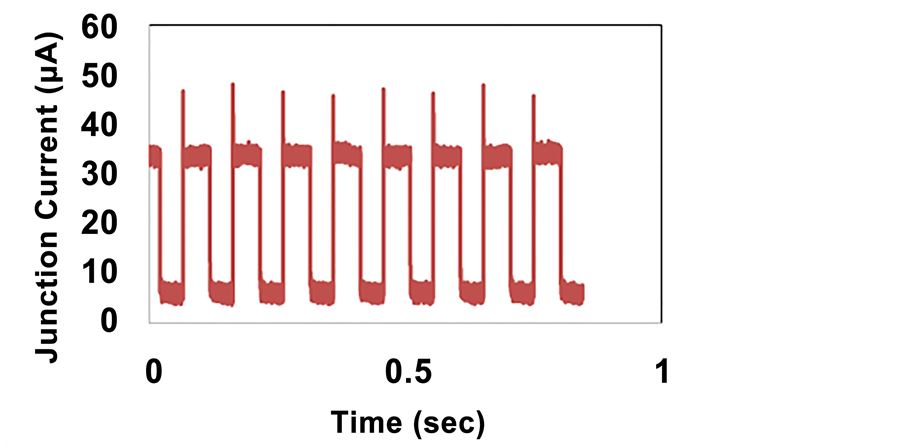
Figure 7. The response of an analogous Ti oxide based junction is shown when exposed to a white LED strobe light.
servoir. The empty surface state can be filled from the left lead. However, the reverse process accompanied by the photon emission would not contribute to the electron current, as electrons cannot be transferred from the ES level to the left reservoir, see Figure 9(b). The ES level is well below the chemical potential of this reservoir and all the states with this energy are already populated. Therefore, the current-voltage characteristics become highly non-symmetrical. The left-to- right current is enhanced because of the additional transport channel, whereas the right-to-left current is not affected by the light illumination. It should be emphasized that the surface states are located closer to the left reservoir than the states inside the HfO layer, so the transfer matrix element for them can be much larger and the current enhancement can be significant. It should be noted that at large applied voltage, when the chemical potential of the left lead is below the
 (a)
(a)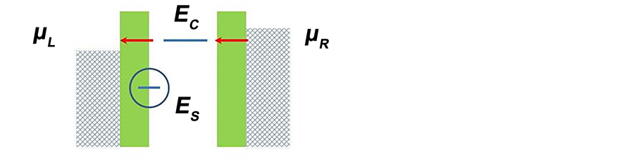 (b)
(b)
Figure 8. Electron transport without light illumination.
 (a)
(a)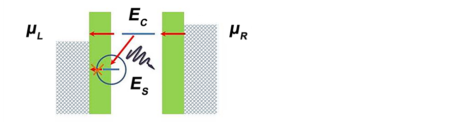 (b)
(b)
Figure 9. Electron transport with light illumination.
level ES, the surface states become involved in transport even at dark via non- radiative relaxation. This process is not symmetric, as it promotes the electron transfer from right to left but not from left to right. It manifests itself in the non- symmetrical current-voltage characteristics of Figure 1 for the dark case.
In this model, several important properties of the original system are omitted. For example, states inside the HfO layer do not have discrete character but rather they are inside a continuous band. We also neglect the particle scattering in the HfO layer, so the electrons transferred to the right reservoir would have smaller energy than just after the photon absorption. Moreover, after the absor- ption of a high-frequency photon, electron would have the energy outside of the conduction window. However, after non-radiative relaxation, the energy is decreased and the electron can proceed to the drain. Nevertheless, we believe that our simple model explains the main features of the observed phenomenology.
A key feature of the geometry shown in Figure 2 is that each junction, or pixel, can be sampled individually by sweeping a bias voltage from junction to junction. It should also be noted that the junction density can be changed by simply increasing the top and or bottom conducting line density without the need for any patterning or changes to the active film layers.
We wish to acknowledge the students Michael Winters, Heriberto Vasquez, and Joseph Monaco assisted in some of the verification measurements. This research was supported in part by PSC-CUNY FRAP grants. The work of L. M. is partially supported by AFOSR, Award No FA9550-16-1-0279, and PSCCUNY, Award No 69365-00 47.
Cite this paper
Cadieu, F.J. and Murokh, L. (2017) Nanometer Thick Diffused Hafnium and Titanium Oxide Light Sensing Film Structures. World Journal of Condensed Matter Physics, 7, 36-45. https://doi.org/10.4236/wjcmp.2017.71004
References
- 1. Cadieu, F.J. (2015) Device with Light-Responsive Layers. US Patent No. 9,040,982.
- 2. Cadieu, F.J. (2014) Device with Light-Responsive Layers. Patent Application Publication No. US 2014/0021468 A1.
- 3. Wilk, G.D., Wallace, R.M. and Anthony, J.M. (1999) Hafnium and Zirconium Silicates for Advanced Gate Dielectrics. Journal of Applied Physics, 87,484.
https://doi.org/10.1063/1.371888 - 4. Callegari, A., Cartier, E., Gribelyuk, M., Okom-Schmidt, H.F. and Zabel, T. (2001) Physical and Electrical Characterization of Hafnium Oxide and Hafnium Silicate Sputtered Films. Journal of Applied Physics, 90, 6466.
https://doi.org/10.1063/1.1417991 - 5. Royal Society of Chemistry 2007, Hafnium Oxide Helps Make Chips Smaller and Faster.
https://www.chemistryworld.com/news/hafnium-oxide-helps-make-chipssmaller-and-faster/1015409.article - 6. Alexandrov, A.S., Bratkovsky, A.M., Bridle, B., Savel’ev, S.E., Strukov, D.B. and Stanley Williams, R. (2011) Current-Controlled Negative Differential Resistance Due to Joule Heating in TiO2. Applied Physics Letters, 99, 202104.
https://doi.org/10.1063/1.3660229 - 7. Chua, L.O. (1971) Memristor-The Missing Circuit Element. IEEE Transactions on Circuit Theory, 507-519.
- 8. Beck, A., Bednorz, J.G., Gerber, Ch., Rossel, C. and Widmer, D. (2000) Reproducible Switching Effect in Thin Oxide Films for Memory Applications. Applied Physics Letters, 77, 139.
https://doi.org/10.1063/1.126902 - 9. Cadieu, F.J., Vander, I., Rong, Y. and Zuneska, R.W. (2012) X-Ray Measurements of Nanometer-Thick Tantalum Oxide and Hafnium Oxide Films on Silicon Substrates for Thickness and Composition Determination. Powder Diffraction, 27, 87-91.
https://doi.org/10.1017/S0885715612000425 - 10. Cadieu, F.J. (1992) Permanent Magnet Thin Films. In: Vossen, J. and Francombe, M., Eds., Physics of Thin Films, Vol. 16, Academic Press, San Diego.
- 11. Cadieu, F.J. (2000) Chapter 1: Magnetic Film Devices Volume of the Handbook on Thin Film Devices Technology and Applications. In: Adam, J.D. and Francombe, M.H., Eds., Permanent Magnet Films for Applications, Academic Press, Inc., San Diego.
- 12. Cadieu, F.J., Vander, I., Rong, Y. and Zuneska, R.W. (2011) Glancing XRD and XRF for the Study of Texture Development in SmCo Based Films Sputtered Onto Silicon Substrates. Advances in X-Ray Analysis, 54-DXC 2010, 162-176 (Denver X-Ray Conf. 2010).
- 13. Sakurai, T. and Sugano, T. (1981) Theory of Continuously Distributed Trap States at Si-SiO2 Interfaces. Journal of Applied Physics, 52, 2889-2896.
https://doi.org/10.1063/1.329023 - 14. Lucovsky, G., Fitch, J.T., Kobeda, E. and Irene, I.E. (1988) Local Atomic Structure of Thermally Grown SiO2 Films. In: Helms, C.R. and Deal, B.E., Eds., The Physics and Chemistry of SiO2 and the Si-SiO2 Interface, Premium Press, New York, 139-148.
https://doi.org/10.1007/978-1-4899-0774-5_15 - 15. Wolkin, M.V., Jorne, J., Fauchet, P.M., Allan, G. and Delerue, C. (1999) Electronic States and Luminescence in Porous Silicon Quantum Dots: The Role of Oxygen. Physical Review Letters, 82, 197.
https://doi.org/10.1103/PhysRevLett.82.197 - 16. Ohtomo, A. and Hwang, H.Y. (2004) A High-Mobility Electron Gas at the LaAlO3/SrTiO3 Heterointerface. Nature, 427, 423.
https://doi.org/10.1038/nature02308 - 17. Eckstein, J.N. (2007) Oxide Interfaces: Watch Out for the Lack of Oxygen. Nature Materials, 6, 473.
https://doi.org/10.1038/nmat1944