Advances in Materials Physics and Chemistry
Vol. 2 No. 3 (2012) , Article ID: 23198 , 5 pages DOI:10.4236/ampc.2012.23020
Fabrication and Characterization of Poly[Decaphenylcyclopentasilane]-Based Solar Cells
1Department of Materials Science, The University of Shiga Prefecture, Hikone, Japan
2Osaka Gas Chemicals Co. Ltd., Osaka, Japan
Email: *oku@mat.usp.ac.jp
Received May 31, 2012; revised July 3, 2012; accepted July 13, 2012
Keywords: PDPS; polysilane; solar cell; amorphous; silicon
ABSTRACT
Poly[decaphenylcyclopentasilane] (PDPS)-based photovoltaic cells were fabricated by using mixture solution of PDPS including boron and phosphorous elements. A doping effect of phosphorus and boron into PDPS was investigated on the performance of the photovoltaic devices. The solar cell provided short-circuit current density of 0.11 mA/cm2 and open-circuit voltage of 0.81 V under simulated sunlight. Microstructural analysis indicated that PDPS had an amorphous structure, which would result in the photovoltaic properties.
1. Introduction
Fossil fuels are widely used on the earth in the present time, and burning fossil fuels affects the natural environment by production of greenhouse gases. Problems of energy supply are related not only to global warming but also to environmental concerns such as air pollution and forest destruction. In addition, fossil fuel is limited, and other energy resources should be developed, and photovoltaic devices are one of the important candidate. Although a mainstream of solar cells is silicon solar cells with a high energy conversion efficiency and long lifetime, they are expensive and heavy. For the next generation solar cells, thin film organic solar cells have been studied since they are inexpensive, flexible and light. Polysilanes have a high hole mobility as organic semiconductors because of its σ-conjugated polymers, and it is possible to use the materials for organic thin film solar cells. Although the polysilanes could be applied to p-type semiconductors for organic thin film solar cells [1-3], few studies on polysilane-based solar cells have been reported [4,5]. On the other hand, polysilanes formed amorphous silicon when annealed at high temperatures.
The purpose of the present study was to fabricate photovoltaic solar cells by using mixture solution of poly[decaphenylcyclopentasilane] (PDPS) doped with phosphorus and boron, and to investigate the effects of annealing temperatures, rotation speed of spin-coating and doping of boron (B) and phosphorous (P) on their electronic properties and microstructures. It is expected that amorphous silicon doped with boron would function as p-type semiconductor, and amorphous silicon doped with phosphorus would function as n-type semiconductor. Spin-coating is a low-cost method, and is essential for mass production of any solar cells. The PDPS solar cells were investigated by structural analysis and measurements of optical absorption and photovoltaic property.
2. Experimental Procedures
A thin layer of polyethylenedioxythiophen-doped with polystyrene-sulfonic acid (PEDOT:PSS) (Sigma Aldrich) was spin-coated on pre-cleaned fluorine doped tin oxide (FTO) glass plates (Luminescence Technology Co. ~14 Ω/□). Then, semiconductor layers were prepared on the PEDOT:PSS layer by spin coating using the mixture solution of PDPS (7 mg, Osaka Gas Chemicals Co., Ltd.) and diethylmethoxyborane (0.2 ml, Sigma Aldrich) in 1 ml o-dichlorobenzene. After annealing at 250˚C for 10 min or 300˚C for 10 min in N2 atmosphere, a subsequent layer was prepared by spin-coating using the mixture solution of PDPS and phosphoric acid (0.2 ml, Sigma Aldrich) in 1 ml o-dichlorobenzene [6-8]. After annealing at 250˚C for 10 min or 300˚C for 10 min in N2 atmosphere, aluminum (Al) metal contacts were evaporated as the top electrode. Rotation speed of semiconductor layers were changed 1000, 500 or 300 rpm. A schematic diagram of the present solar cells is shown in Figure 1.

Figure 1. Structure of the present solar cells.
The current density-voltage (J-V) characteristics (Hokuto Denko, HSV-110) of the solar cells were measured under illumination at 100 mW/cm2 by using an AM 1.5 solar simulator (San-ei Electric, XES-301S). The solar cells were illuminated through the side of the FTO substrates, and the illuminated area was 0.16 cm2. Optical absorption of the solar cells was investigated by means of UV-visible spectroscopy (JASCO, V-670ST). The microstructures of the PDPS thin films were investigated by X-ray diffractometry (XRD, Philips X’Pert-MPD System) with CuKa radiation at 40 kV operating voltage and 40 mA operating current. Transmission electron microscope observation was carried out by a 200 kV TEM (Hitachi H-8100).
3. Results and Discussion
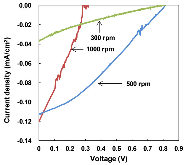
Measured J-V characteristic of PDPS(B)/PDPS(P) solar cells prepared at 300˚C is shown in Figure 2. Measured parameters of the present solar cells prepared at 300˚C and 250˚C are summarized in Table 1.
Photocurrents were observed under the illumination, and each structure showed characteristic curves with short-circuit current and open-circuit voltage. The solar cells prepared at 300˚C showed better short-circuit current compared to that prepared at 250˚C. The cell fabricated at 500 rpm and annealed at 300˚C provided the highest power conversion efficiency (η) of 0.028 %, fill factor (FF) of 0.28, short-circuit current density (Jsc) of 0.11 mA/cm2 and open-circuit voltage (Voc) of 0.81 V. A PDPS(P) solar cell provided low η, and PDPS(B) showed no photovoltaic response.
A heterojunction structure of PDPS(B)/ PDPS(P) provided higher efficiencies in the present work, which indicates formation of pn junction. The pin heterojunction solar cells were also investigated, and a higher efficiency was obtained at higher rotation speed of spin-coating, which suggests that thinner i layers of PDPS is preferred.
Figure 3 shows optical absorption spectra of PDPS (B)/PDPS(P) thin films fabricated at rotation speed of 1000 rpm. The cell annealed at 300˚C shows higher optical absorption compared to that annealed at 250˚C.
 (a)
(a)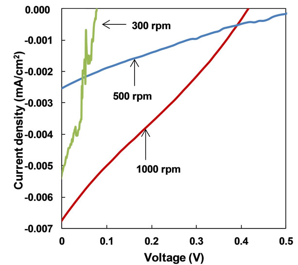 (b)
(b)
Figure 2. J-V characteristic of FTO/PEDOT:PSS/PDPS(B) PDPS(P)/Al solar cells prepared by annealing at (a) 300˚C and (b) 250˚C.
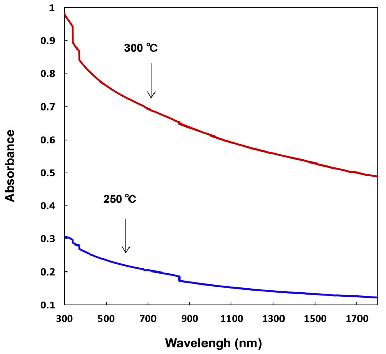
Figure 3. Absorption spectra of PDPS(B)/PDPS(P) heterojunction films after annealing at 250˚C and 300˚C.

Table 1. Measured parameters of the present solar cells.
Broad optical absorption observed in Figure 3 would be due to light scattering of PDPS.
X-ray diffraction patterns of the annealed PDPS thin films are shown in Figure 4. Some diffraction peaks were observed in the PDPS after annealing at 250˚C, which indicates microcrystalline structures, and the crystallite size is ~180 nm. After annealing at 300˚C, most of the diffraction peaks decreased and disappeared in the PDPS(B) and PDPS(P) thin films, which indicates formation of an amorphous structure from the microcrystalline structure. Addition of phosphoric acid and diethylmethoxyborane to PDPS would also enhance the decomposition of the PDPS to the amorphous structure.
Figure 5(a) is a high-resolution electron microscope (HREM) image of PDPS annealed at 300˚C, and Figure 5(b) is an electron diffraction pattern of the PDPS. Image
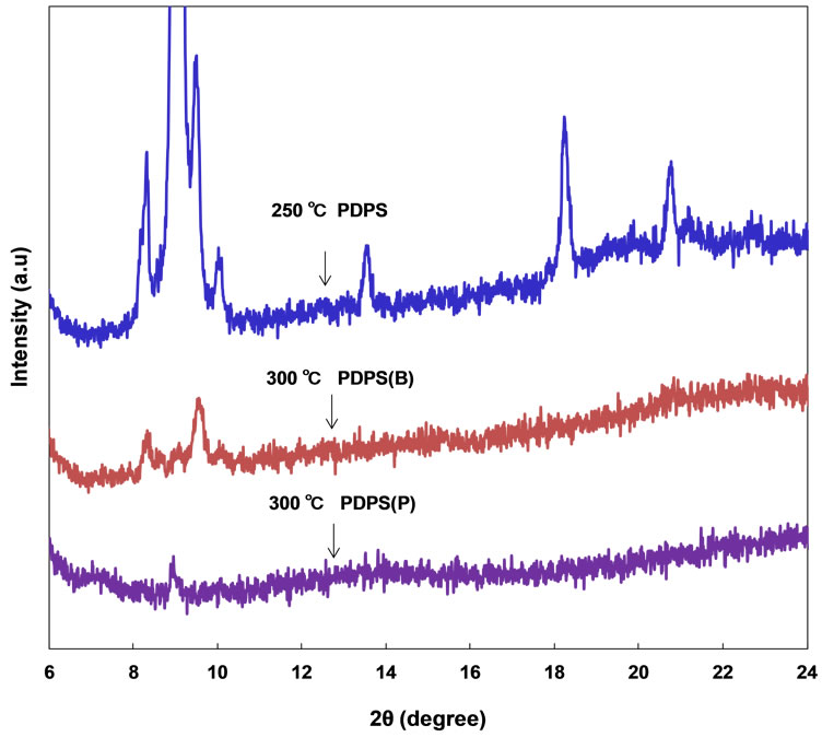
Figure 4. XRD patterns of PDPS thin films with phosphorus and boron after annealing.
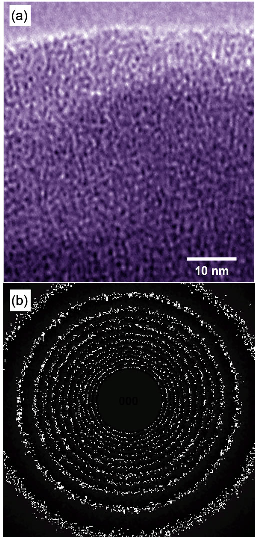
Figure 5. (a) HREM image and (b) electron diffraction pattern of PDPS thin film after annealing at 300˚C.
contrast corresponding to an amorphous structure is observed in Figure 5(a), and Figure 5(b) showed hallo-like intensity, which indicates that PDPS annealed at 300˚C had an amorphous structure.
A schematic illustration of heat treatment of PDPS is summarized as shown in Figure 6. The JSC of PDPS annealed at 300˚C is higher compared to that annealed at 250˚C. The 3-dimensional amorphous network of silicon with doping atoms would transport the carriers in the cells. Decomposition of the PDPS into the amorphous structure would be due to not only temperature of 300˚C, but also addition of phosphoric acid and diethylmethoxyborane to PDPS. To improve the efficiency, control of atomic structures by annealing and doping should be investigated further [9].
Proposed energy level diagram of the present solar cells is summarized as shown in Figure 7. Amorphous silicon doped with boron or phosphorus would function as p-type or n-type semiconductor, respectively [10]. Energy levels would be different between PDPS with B and PDPS with P, and previously reported values were used for the energy levels [11,12]. The incident of light is from ITO or FTO side. Electronic charge separation was caused by light irradiation from the ITO or FTO substrate side. Separated holes could be transferred from the valence band of Si doped with B to the ITO or FTO, and separated electrons could be transferred from the conduction band of Si doped with P to the Al electrode. In
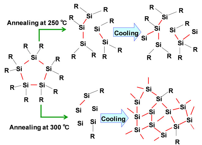
Figure 6. Schematic model of structural change during annealing.
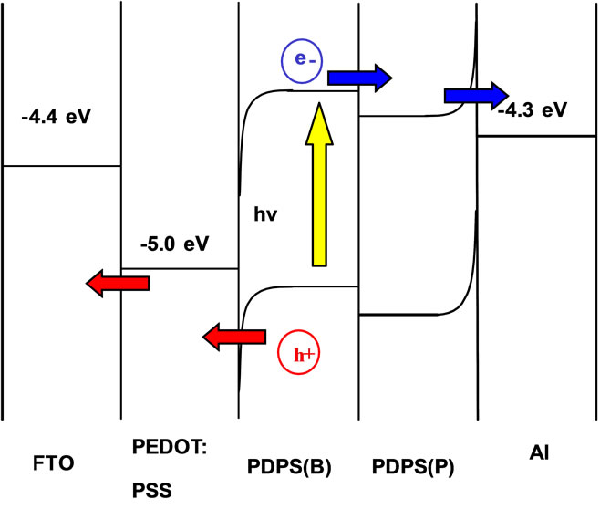
Figure 7. Energy level diagram of FTO/PEDOT:PSS/PDPS (B)/PDPS(P)/Al solar cells.
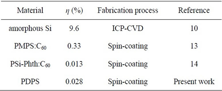
Table 2. Comparison of silicon-based solar cells.
addition, there would be energy barrier at the semiconductor/metal interfaces as indicated by band bending in Figure 7, and heavy doping of B or P would reduce the contact resistance.
The present PDPS-based solar cells were compared with other silicon-based solar cells [10,13,14] such as amorphous silicon solar cells prepared by inductively coupled plasma chemical vapor deposition (ICP-CVD) and spin coating method, as listed in Table 2. The present solar cells fabricated by spin-coating have simple fabrication process and better cost performance. Low conversion efficiency of the present solar cells would be due to high electrical resistance and carrier recombination by defects, and further improvement is mandatory.
4. Conclusion
Polysilane-based solar cells were fabricated by using mixture solution of PDPS, phosphorus and boron, and characterized by electrical measurements and microstructural analysis. A device fabricated at 500 rpm and at 300˚C provided η of 0.028%, FF of 0.28, JSC of 0.11 mA/cm2 and Voc of 0.81 V. XRD and TEM results indicated that PDPS formed an amorphous structure by annealing at 300˚C. Energy levels of the molecules and carrier transport mechanism were discussed.
REFERENCES
- M. Kakimoto, H. Kashihara, T. Kashiwagi and T. Takiguchi, “Visible Light Photoconduction of Poly(disilanyleneoligothienylene)s and Doping Effect of C60,” Macromolecules, Vol. 30, No. 25, 1997, pp. 7816-7820. doi:10.1021/ma960832a
- J. Lee, C. Seoul, J. Park and J. H. Youk, “Fullerene/ Poly(methylphenylsilane) (PMPS) Organic Photovoltaic Cells,” Synthetic Metals, Vol. 145, No. 1, 2004, pp. 11-14. doi:10.1016/j.synthmet.2004.04.022
- Y. Haga and Y. Harada, “Photovoltaic Characteristics of Phthalocyanine-Polysilane Composite Films,” Japanese Journal of Applied Physic, Vol. 40, 2001, pp. 855-861. doi:10.1143/JJAP.40.855
- A. Watanabe and O. Ito, “Photoinduced Electron Transfer between C60 and Polysilane Studied by Laser Flash Photolysis in the Near-IR Region,” The Journal of Physical Chemistry, Vol. 98, No. 31, 1994, pp. 7736-7740. doi:10.1021/j100082a052
- M. Iwase, T. Oku, A. Suzuki, T. Akiyama, K. Tokumitsu, M. Yamada and M. Nakamura, “Fabrication and Characterization of Poly[diphenylsilane]-Based Solar Cells,” Journal of Physics: Conference Series, Vol. 352, No. 1, 2012, Article ID: 012018. doi:10.1088/1742-6596/352/1/012018
- T. Shimoda, Y. Matsuki, M. Furusawa, T. Aoki, I. Yudasaka, H. Tanaka, H. Iwasawa, D. Wang, M. Miyasaka and Y. Takeuchi, “Solution-Processed Silicon Films and Transistors,” Nature, Vol. 440, 2006, pp. 783-786. doi:10.1038/nature04613
- Y. Matuki. H. Iwasawa. D. Wang. Y. Koshikiya and T. Simoda, “Solution-Processed Silicon Films and Transistors,” JSR Technical Review, Vol. 114, 2007, pp. 16-22.
- S. Kim, C. Lee and M. H. Jin, “Fourier-Transform Infrared Spectroscopic Studies of Pristine Polysilanes as Precursor Molecules for the Solution Deposition of Amorphous Silicon Thin-Films,” Solar Energy Materials and Solar Cells, Vol. 100, 2012, pp. 61-64. doi:10.1016/j.solmat.2011.04.023
- G. Raabe and J. Michl, “Multiple Bonding to Silicon,” Chemical Reviews, Vol. 85, No. 5, 1985, pp. 419-509. doi:10.1021/cr00069a005
- H. Tanaka, H. Iwasawa, D. Wang, N. Toyoda, T. Aoki, I. Yudasaka, Y. Matsuki, T. Shimoda and M. Furusawa, “Spin-On n-Type Silicon Films Using PhosphorousDoped Polysilanes,” Japanese Journal of Applied Physic, Vol. 46, 2007, pp. L886-L888. doi:10.1143/JJAP.46.L886
- T. Oku, R. Motoyoshi, K. Fujimoto, T. Akiyama, B. Jeyadevan and J. Cuya, “Structures and Photovoltaic Properties of Copper Oxides/Fullerene Solar Cells,” Journal of Physics Chemistry of Solids, Vol. 72, No. 11, 2011, pp. 1206-1211. doi:10.1016/j.jpcs.2011.06.014
- T. Oku, T. Noma, A. Suzuki, K. Kikuchi and S. Kikuchi, “Fabrication and Characterization of Fullerene/Porphyrin Bulk Heterojunction Solar Cells,” Journal of Physics Chemistry of Solids, Vol. 71, No. 4, 2010, pp. 551-555. doi:10.1016/j. jpcs.2009.12.034
- H. Y. Jung, L. Y. Chien, S. Chang-Hong, S. Jia-Min and D. Bau-Tong, “Low Cost High-Efficiency Amorphous Silicon Solar Cells with Improved Light-Soaking Stability,” Solar Energy Materials and Solar Cells, Vol. 98, 2012, pp. 277-282. doi:10.1016/j.solmat.2011.11.023
- A. Rybak, J. Jung, W. Ciesielski and J. Ulanski, “Photovoltaic Effect in Novel Polysilane with Phenothiazine Rings and Its Blends with Fullerene,” Materials Science Poland, Vol. 24, 2006, pp. 527-534.
NOTES
*Corresponding author.