Advances in Materials Physics and Chemistry
Vol.3 No.1(2013), Article ID:29121,6 pages DOI:10.4236/ampc.2013.31004
Theoretical Investigation of Electronic and Optical Properties of Si/SiGe Quantum Cascade Structures
1Applied Materials Laboratory (AML), University of Sidi Bel Abbès, Sidi Bel Abbès, Algeria
2Laboratoire de Dispositifs de Communication Conversion Photovoltaique, Ecole Nationale Polytechnique, Algiers, Algeria
Email: zellat_samira@yahoo.fr
Received January 4, 2013; revised February 5, 2013; accepted February 24, 2013
Keywords: SiGe Alloy; Electronic and Optical Properties; Quantum Cascade Lasers (QCLs)
ABSTRACT
This paper reviews the basic properties of the SiGe alloy, presents some new results on its electronic and optical properties, and discusses the approach that has been followed to model quantum wells containing SiGe layers for applications in quantum cascade lasers. The shape of the confining potential, the subband energies and their eigen envelope wave functions are calculated by solving a one-dimensional Schrödinger equation. The calculations of optical parameters are used to optimize the Si/SiGe quantum cascade structures. Our results are found to be in good agreement with other calculations.
1. Introduction
A quantum cascade laser (QCLs) is a specific type of semiconductor laser that operates through principles of quantum mechanics. Already theoretically predicted in 1971 [1], QCLs had not been realized until 1994 at Bell Laboratories [2]. They have many advantages over other types of semiconductors’ lasers. Some of these advantages include precise tuning from one wavelength to another, higher optical power, continuous wave operation and the ability to produce light in the terahertz range of the spectrum [3-6].
From the physical point of view, the unipolarity of a QC laser indicates that electrons are solely responsible for releasing energy in the form of photons. These electrons transition from one quantum energy state to another within a layer, or group of layers, of semiconductor material releasing energy in the form of photons during their descent. The binding energy necessary to pull these electrons away from the Coulombic force of the nucleus in the atom is related to the extremely thin semiconductor layers. A property of quantum mechanics known as quantum confinement occurs when the electrons are trapped within a thin semiconductor quantum well layer. These electrons can freely move in only two directions within the plane of the thin layer. In this case quantum confinement, which leads to discrete energy levels that electrons can occupy in a material smaller than the de Broglie wavelength, occurs in only one dimension due to the quantum well structure [7]. Unlike the earliest form of semiconductor lasers where the energy bandgap determines the wavelength of the light emitted, with QC lasers the thickness of the layers determines the wavelength. This is a critically important property of QC lasers because it allows them to be tuned to a desired frequency through bandgap engineering [8]. Technologically speaking, this laser type is grown by epitaxial method such as molecular beam epitaxy (MBE) [9]. Layers of different semiconductor materials each only a few atomic layers thin are deposited onto a thin slice of a semiconductor crystal. In order to optimize the electronic wave functions with respect to energy and probability distribution, we have to choose the sequence of the layers, their width and materials.
It was established that these unipolar intersubband lasers might be realized not only in III-V semiconductors [10-13] but also in IV-IV structures [14-16]. Among semiconductors, the covalent semiconductors Si and Ge have been studied extensively both theoretically and experimentally [17,18]. Group IV semiconductors alloys like Si-Ge, have the immense potential for technological applications whose include the optoelectronic devices [19-21]. By using intersubband transitions within the same band, one can circumvent the main obstacle to silicon-based lasers, the indirect band gap. The large band offsets in the valence band of pseudomorphic SiGe layers on Si substrates imply a quantum cascade scheme with hole subbands.
In our previous publication [22], we were interested to the investigation of the structural, electronic and optical properties of Si, Ge, and Si1–xGex for different compositions using the full-potential linear muffin-tin orbital (FP-LMTO) method augmented by a plane-wave basis (PLW), implemented in Lmtar code [23-25]. All the obtained results showed that the weakly strained G-rich SiGe layers possess very promising properties for both electronic and optical applications.
The aim of the present work is to provide a consistent and complete set of electronic and optical parameters of the Si/SiGe quantum well. The obtained results are going to be of use to a good understanding of the quantum phenomena of these devices. The second objective concerns the way which allows us to optimize the intrinsic parameters of the Si/SiGe quantum cascade structure.
2. Method of Calculations
Much theoretical work has been done to accompany the rapid experimental developments of QCLs as well as to better explain the design considerations of intersubband lasers. These include Monte Carlo simulations [26-29], self-consistent rate equations [30,31], as well as the nonequilibrium Green’s function formalism [32,33]. As was shown above, the quantum cascade lasers (QCL’s) are fabricated by stacking up alternating layers of semiconducting material with nanoscale thicknesses. This heterostructure of layers forms a series of conductionband quantum wells in the z direction which trap the electrons into subband states [2] (Figure 1). The calculation procedures described here follows the envelope function approach based on the effective-mass approximation [34,35]. This approximation was found to be much more computationally efficient than atomistic methods, making it more suitable as a design tool for QCLs [36].
The eigenstate of an electron in the unperturbed Hamiltonian of a QCL is the product of the Bloch envelope function B(x, y, z), the free electron wavefunction in the x and y direction, and the bound quantum-well eigen-functions ψn(z) in the z direction.
The Bloch function factor contains the effects on the electron state due to the non-uniform nature of the crystal potential on the atomic scale.
We assume the semiconductor layer widths are large compared to the atoms, so we make the approximation that the Bloch function factor is negligible. Each electron is pseudo-free in the x and y dimensions because the material is uniform in those dimensions. Even though each electron is bound to the crystal in these dimensions, we can treat each as free if we use the effective mass of the electron. The bound-state z component wave functions ψn(z) are found by numerically solving the one-dimensional Schrödinger equation when the potential profile is known. The potential profile is a combination of the
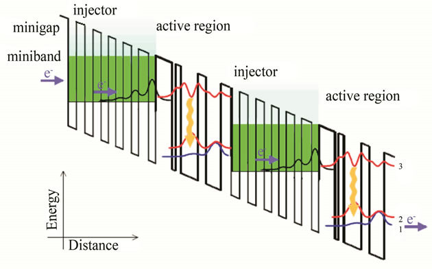
Figure 1. Conduction band profile in two adjacent stages of a generic QCL under an applied bias.
conduction-band edge quantum well profile of the material layers, the bias voltage, and the built-in potential which accounts for the effects of space charge. This minimum energy can be calculated as one of the eigen values of the Schrödinger equation along the growth direction z,
 (1)
(1)
where h is the Planck constant and Ei is the minimum energy of subband i in a QW structure. By solving this equation, one obtains the energy Ei (eigenvalues) and the wave function ψn (eingenfunctions) of the n electron state. In this method, we have taken into account the boundary conditions for the wavefunction.
An analytical solution provided by solving the Schrö- dinger equation for the conduction minimum energy of subband i has the following form Bas du formulaire
 (2)
(2)
Haut du formulaire where Lz represent the depth of the quantum well.
Bas du formulaire.
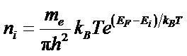
For a given temperature T, the population ni for each subband i is expressed by
 (3)
(3)
Two simplified expressions can be established for the population ni:
For the subband situated below the Fermi level  , the population is
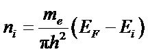 .
.
For the subband situated above the Fermi level
 , the population becomes
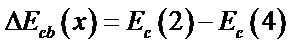
Haut du formulaire The effective states density according to x concentration for the Si/SiGe quantum well is given by
 (4)
(4)
where ΔEcb is the limit energy of the conduction band which is differentiated in two terms Ec(2) and Ec(4). Ec(2) is the value linked to both identical directions [001] and [001] while Ec(4) is the value linked to the four other identical directions [010], [010], [100] et [100].
Bas du formulaire We have then
with
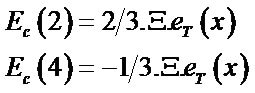
The term eT(x) is the difference between the strain tensors ezz – exx, according to directions zz and xx. These strain tensors depend of the silicon lattice parameter as well as the SiGe bowing parameter.
3. Results and Discussions
To design a desired QW structure such as the quantum cascade laser and improve a device performance, a numerical simulation is needed to compute the energy levels and for different electrons states, the corresponding envelope functions, the intersubband transition dipole moments, carrier densities, relaxation times and other parameters. Then, subband formation and energy dispersion are described in the framework of envelope functions with the effective-mass approximation for both conduction and valence band. In Figure 2, we displayed the profiles of the envelope function for different electron states.
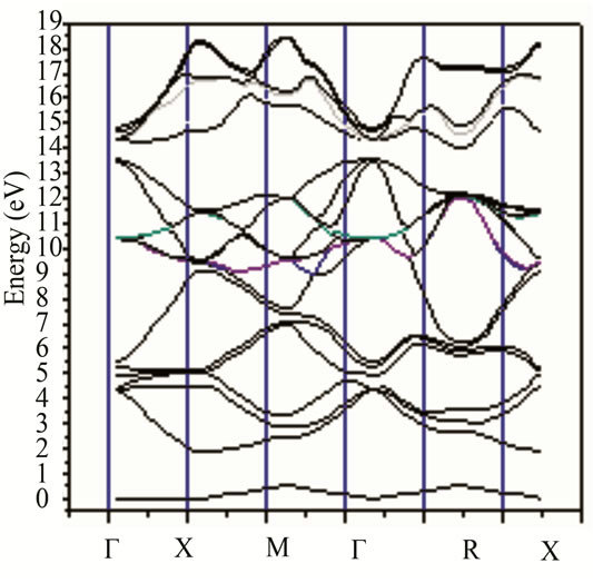
In Figure 3, we have illustrated the calculated electronic energy-band structure (a) and total DOS (b) of Si1–xGex alloy for x = 0.5. For the calculations, we have used the full-potential linear muffin-tin orbital (FP-LMTO) method augmented by a plane-wave basis (PLW), implemented in Lmtar code [23-25]. The effects of the approximations to the exchange-correlation energy were treated by the local density approximation (LDA).
Figure 4 shows the variation of the confinement energy with respect to different width wells. This energy is carried out by solving the Schrodinger equation for the Si/SiGe quantum cascade structure. It is clear from this
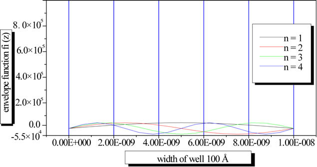
Figure 2. The profiles of the envelope function for different electron states.
 (a)
(a) (b)
(b)
Figure 3. The calculated electronic energy-band structure (a) and total DOS (b) of Si1−xGex alloy for x = 0.5.

Figure 4. The confinement energy vs the width well for different states.
results that for the low width wells the confinement energy is very important. This leads favorably to the intersubband transition. Hence, the emitted wavelength of the QCL only depends on the thicknesses of the layers. One can notice that the use of semiconductor with small effective mass excites well the confinement effects what is not the case for the material SiGe of which its effective mass is important compared to those of GaAs, InAs, equal to 0.067 m0 and 0.023 m0, respectively.
Figure 5 illustrated the variation of the effective states density with respect to germanium concentration x. We can see that the effective states density of the barrier material is very important to that of the well. Then we shall have continued and a strong carrier’s injection in the well to minimize the losses and increase the laser gain.
Figure 6, shows the relative position of minibands for two consecutive transport zones under an applied bias for our quantum cascade structure. By varying the thickness of the wells and barriers of the Si/SiGe super lattice, we modify the position and the size of these minibands. We can extract from this scheme the main functions of the transport zone, which guarantees, the transport of electrons towards the excited subband of the emission zone, the blocking by the miniband gap of the electrons transport of the excited subband towards the continuum, causing then the electron excitations by the inter subband transition. The next step is the injection of the extracted carriers from the fundamental subband towards the next emission zone.
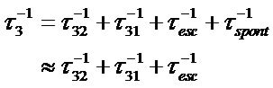
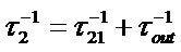
Let us to turn now to the description of the electronic relaxation process with the aim of showing the various rates occurring to describe the intersubband transitions. We consider an emission zone with 3 subbands where the intersubband transition 3 - 2 being radiative. Figure 7 schematizes the various interactions involve for the period where J is the current density, η3 is the current injection efficiency in the subband 3 and η1,2 the propor-

Figure 5. The effective states density vs the germanium concentration x.
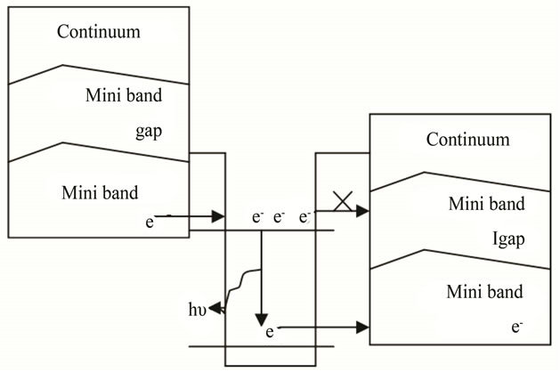
Figure 6. The relative position of minibands for two consecutive transport zones under an applied bias.
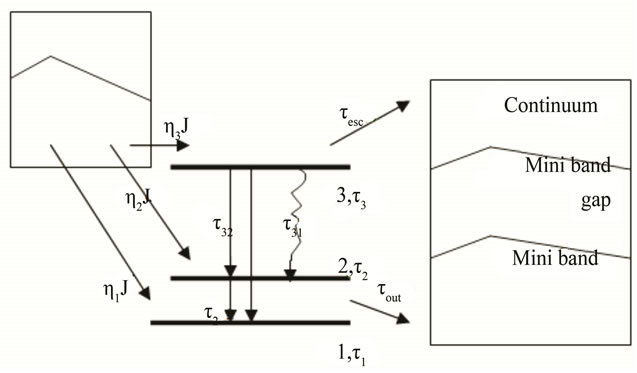
Figure 7. The schematic of the electronic relaxation process.
tions of current of flight (leak) in subbands 1 and 2.
In the present model, we shall suppose that the injection is completed (η3 = 100%). Each subband is associated a life time of electrons noted ti, i = 1, 2, 3. The Electron-phonon interaction was represented by the rate  for an electron transition from the subband i towards the subband j. The electron escape rate towards the continuum was represented by
 . Finally
  denotes the extraction rate of electrons in the miniband of the following transport zone.
According to these notations [3], the electronic relaxation process is then describes by the following equations:
 (5)
(5)
For lasing to occur between two subbands, it is necessary to induce stimulated emission between them. To sustain such emission of photons, there must be sufficient optical gain to compensate various losses in the laser structure. The intersubband optical gain can be obtained by analyzing transition rates between two subbands.
We note that the optimization of the active zone has for an essential purpose to control the electrons phonons interactions, the injection and the extraction of the carriers from the emission zone to the other one and to maximize the strength of oscillator of the radiative transition of this QCL. It is found that the oscillator strength, in the case of our considered system Si/SiGe, corresponding to the intersubband transition between the sub states i and j depends only on the electron effective mass. Hence, a high intersubband optical gain requires a high oscillator strength.
On the other hand, the optical gain is very sensitive to the values of the width well and the doping of the wave guide used in this structure.
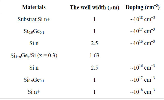
In Table 1, we have listed the optimized parameters for our waveguide based on the Si1–xGex/Si system. These results are in good agreement with other calculation [37].
4. Conclusions
In this paper, we have carried out the background knowledge necessary to appreciate the quantum cascade laser structure and operation. It begins with a discussion of laser fundamentals and quantum wells and concludes with information on Si1–xGex/Si QC Lasers.
The shape of the confining potential, the subband en-
Table 1. The optimized parameters for the Si1–xGex/Si wave guide.
ergies and their eigen envelope wave functions are calculated by solving a one-dimensional Schrödinger equation. The calculation of optical parameters is used to optimize the Si/SiGe quantum cascade structures. Our results are found to be in good agreement with other calculations. Further works are in progress.
REFERENCES
- R. F. Kazarinov and R. A. Suris. “Possibility of the Amplification of Electromagnetic Waves in a Semi-Conductor with a Superlattice,” Soviet Physics, Semi-Conductors, Vol. 5, No. 4, 1971, p. 707.
- J. Faist, F. Capasso, D. Sivco ,C. Sirtori, A. L. Hutchinson and A. Y. Cho, “Quantum Cascade Laser,” Science, Vol. 264, No. 5158, 1994, pp. 553-556. doi:10.1126/science.264.5158.553
- J. Faist, F. Capasso, C. Sirtori, D. Sivco and A. Cho, “Intersubband Transitions in Quantum Wells: Physics and Device Applications II,” Academic Press, New York, 2000, pp. 1-83.
- F. Capasso, C. Gmachl, D. L. Sivco and A. Y. Cho. Physics World, Vol. 12, 1999, p. 27.
- J. Faist, M. Beck, T. Aellen and E. Gini, “Quantum-Cascade Lasers Based on a Bound-to-Continuum Transition,” Applied Physics Letters, Vol. 78, No. 2, 2001, pp. 147-149.
- H. Page, C. Becker, A. Robertson, G. Glastre, V. Ortiz and C. Sirtori, “300 K Operation of a GaAs-Based Quantum-Cascade Laser at λ ≈ 9 μm,” Applied Physics Letters, Vol. 78, No. 22, 2001, pp. 3529-3531.
- C. J. Otten, “For Quantum Confinement, Size Matters, But So Does Shape,” Washington University, St. Louis, 2003.
- M. Fukuda, “Optical Semiconductor Devices,” John Wiley and Sons, Inc., New York, 1999.
- F.-Q. Liu, L. Li, L. J. Wang, J. Q. Liu, W. Zhang, Q. D. Zhang, W. F. Liu, Q. Y. Lu and Z. Wang, “Solid Source MBE Growth of Quantum Cascade Lasers,” Applied Physics A, Vol. 97, No. 3, 2009, pp. 527-532. doi:10.1007/s00339-009-5423-8
- C. Sirtori, P. Kruck, S. Barbieri, P. Collot, J. Nagle, M. Beck, J. Faist and U. Oesterle, “GaAs/AlxGa1−xAs Quantum Cascade Lasers,” Applied Physics Letters, Vol. 73, No. 24, 1998, p. 3486. doi:10.1063/1.122812
- F. Capasso, C. Gmachl, A. Tredicucci, A. L. Hutchinson, D. L. Sivco and A. Y. Cho, “High Performance Quantum Cascade Lasers,” Optics and Photonics News, Vol. 10, No. 10, 1999, p. 31. doi:10.1364/OPN.10.10.000031
- C. Gmachl, F. Capasso, R. K. Rohler, A. Tredicucci, A. L. Hutchinson, D. L. Sivco, J. N. Baillargeon and A. Y. Cho, “Mid-Infrared Tunable Quantum Cascade Lasers for GasSensing Applications,” IEEE Circuits Devices, Vol. 16, No. 3, 2000, pp. 10-18. doi:10.1109/101.845908
- C. R. Webster, G. J. Flesch, D. C. Scott, J. E. Swanson, R. D. May, W. S. Woodword, C. Gmachl, F. Capasso, D. L. Sivco, J. N. Baillargeon, A. L. Hutchinson and A. Y. Cho, “Quantum-Cascade Laser Measurements of Stratospheric Methane and Nitrous Oxide,” Applied Optics, Vol. 40, No. 3, 2001, p. 321. doi:10.1364/AO.40.000321
- G. Dehlinger, L. Diehl, U. Genser, H. Sigg, J. Faist, K. Ensslin, D. Grutzmacher and E. Muller. Science, Vol. 290, p. 2277.
- I. Bormann, K. Brunner, S. Hackenbuchner, G. Zandler, G. Abstreiter, S. Schmult and W. Wegscheider, “Nonradiative Relaxation Times in Diagonal Transition Si/SiGe Quantum Cascade Structures,” Applied Physics Letters, Vol. 80, 2003, p. 5371.
- I. Bormann, K. Brunner, S. Hackenbuchner, G. Abstreiter, S. Schmult and W. Wegscheider, “Nonradiative Relaxation Times in Diagonal Transition Si/SiGe Quantum Cascade Structures,” Applied Physics Letters, Vol. 83, No. 26, 2003, p. 5371. doi:10.1063/1.1631381
- J. C. Phillips, “Bonds and Bands in Semiconductors,” Academic Press, New York, 1973.
- A. R. Jivani, P. N. Gajjar and A. R. Jani, “Total Energy, Equation of States and Bulk Modulus of Si and Ge,” Semiconductor Physics, Quantum Electronics and Optoelectronics, Vol. 5, No. 3, 2002, pp. 243-246.
- T. Soma, “The Electronic Theory of SiGe Solid Solutions,” Physica Status Solidi (b), Vol. 95, No. 2, 1979, pp. 427-431. doi:10.1002/pssb.2220950212
- S. Gonazalez, “Empirical Pseudopotential Method for the Band Structure Calculations of Strained Silicon Germanium Materials,” Ph.D. Thesis, Arizona State University, Arizona, 2001.
- C. J. Williams, “Impact ionization and Auger Recombination in SiGe Heterostructures,” Ph.D. Thesis, University of Newcastle, Tyne, 1996.
- K. Zellat, B. Soudini, N. Sekkal and S. M. Ait Cheikh, “Computational Investigation of Electronic and Optical Properties of Si, Ge, and Si1−xGex Alloys Using the FPLMTO Method Augmented by a Plane-Wave Basis,” American Journal of Condensed Matter Physics, Vol. 2, No. 1, 2012, pp. 1-10. doi:10.5923/j.ajcmp.20120201.01
- S. Y. Savrasov, “Linear-Response Theory and Lattice Dynamamics: A Muffin-Tin-Orbital Approach,” Physical Review B, Vol. 54, No. 23, 1996, pp. 16470-16486. doi:10.1103/PhysRevB.54.16470
- S. Savrasov and D. Savrasov, “Full-Potential LinearMuffin-Tin-Orbital Method for Calculating Total Energies and Forces,” Physical Review B, Vol. 46, No. 19, 1992, pp. 12181-12195. doi:10.1103/PhysRevB.46.12181
- D. Rached, M. Rabah, N. Benkhettou, M. Driz and B. Soudini, “Calculated Band Structures and Optical Properties of Lead Chalcogenides PbX (X = S, Se, Te) under Hydrostatic Pressure,” Physica B: Physics of Condensed Matter, Vol. 337, No. 1-4, 2003, pp. 394-403. doi:10.1016/S0921-4526(03)00443-5
- R. C. Iotti and F. Rossi, “Nature of Charge Transport in Quantum-Cascade Laser,” Physical Review Letters, Vol. 87, No. 14, 2001, Article ID: 146603. doi:10.1103/PhysRevLett.87.146603
- F. Compagnone, A. DiCarlo and P. Lugli, “Monte Carlo Simulation of Electron Dynamics in Superlattice Quantum Cascade Lasers,” Applied Physics Letters, Vol. 80, No. 6, 2002, p. 920. doi:10.1063/1.1448664
- H. Callebaut, S. Kumar, B. S. Williams, Q. Hu and J. L. Reno, “Importance of Electron-Impurity Scattering for Electron Transport in Terahertz Quantum-Cascade Lasers,” Applied Physics Letters, Vol. 84, No. 5, 2004, p. 645. doi:10.1063/1.1644337
- O. Bonno, J. L. Thobel, and F. Dessenne, “Modeling of Electron-Electron Scattering in Monte Carlo Simulation of Quantum Cascade Lasers,” Journal of Applied Physics, Vol. 97, No. 4, 2005, Article ID: 043702. doi:10.1063/1.1840100
- D. Indjin, P. Harrison, R. W. Kelsall and Z. Ikonić, “SelfConsistent Scattering Theory of Transport and Output Characteristics of Quantum Cascade Lasers,” Journal of Applied Physics, Vol. 91, No. 11, 2002, p. 9019. doi:10.1063/1.1474613
- V. D. Jovanovic, D. Indjin, N. Vukmirovic, Z. Ikonic, P. Harrison and E. H. Linfield, “Mechanisms of Dynamic Range Limitations in GaAs/AlGaAs Quantum-Cascade Lasers: Influence of Injector Doping,” Applied Physics Letters, Vol. 86, No. 21, 2005, Article ID: 211117. doi:10.1063/1.1937993
- S. C. Lee and A. Wacker, “Nonequilibrium Green’s function Theory for Transport and Gain Properties of Quantum Cascade Structures,” Physical Review B, Vol. 66, No. 24, 2002, Article ID: 245314. doi:10.1103/PhysRevB.66.245314
- S. C. Lee, F. Banit, M. Woerner and A. Wacker, “Quantum Mechanical Wavepacket Transport in Quantum Cascade Laser Structures,” Physical Review B, Vol. 73, No. 24, 2006, Article ID: 245320. doi:10.1103/PhysRevB.73.245320
- S. R. White and L. J. Sham, “Electronic Properties of Flat-Band Semiconductor Heterostructures,” Physical Review Letters, Vol. 47, No. 12, 1981, pp. 879-882. doi:10.1103/PhysRevLett.47.879
- S. L. Chuang, “Physics of Optoelectronic Devices,” Wiley Interscience, New York, 1995.
- P. Harrison, “Quantum Wells, Wires and Dots,” 2nd Edition, Wiley, Chichester, 2005.
- G. Dehlinger, L. Diehl, U. Gennser, H. Sigg, J. Faist, K. Ensslin, D. Grützmacher and E. Müller, “Intersubband Electroluminescence from SiGe Quantum Cascade Structures,” Science, Vol. 290, 2000, p. 2277.