Optics and Photonics Journal
Vol.06 No.10(2016), Article ID:71555,14 pages
10.4236/opj.2016.610028
Photomechanical Ablation of 304L Stainless Steel, Aluminum Oxide (Al2O3) Thin Film, and Pure Silicon
Gabriel de la Rosa-Santana1, Jose Alfredo Alvarez-Chavez2, Hector R. Morano-Okuno1, Angel J. Morales-Ramirez2, Esmeralda Uribe3
1Instituto Tecnologico y de Estudios Superiores de Monterrey, Campus Estado de Mexico, Atizapan de Zaragoza, Mexico
2Instituto Politecnico Nacional-Centro de Investigacion e InnovacionTecnologica (CIITEC-IPN), Mexico City, Mexico
3Instituto Tecnologico y de Estudios Superiores de Monterrey, Campus Queretaro, Santiago de Queretaro, Mexico

Copyright © 2016 by authors and Scientific Research Publishing Inc.
This work is licensed under the Creative Commons Attribution International License (CC BY 4.0).
http://creativecommons.org/licenses/by/4.0/


Received: August 29, 2016; Accepted: October 24, 2016; Published: October 27, 2016
ABSTRACT
Recently, a number of studies have focused on micro-manufacturing processes, which find use in a variety of applications, including the production of microelectromechanical systems (MEMS). The process of ablation in materials is mainly governed by the laser source and scanning speed. The rate of material ablation is influenced by chemical and physical properties. In this work, the energy from a CO2 laser was used to ablate three different materials, namely, stainless steel 304L, a thin film of amorphous aluminum oxide (Al2O3), and pure silicon, due to their wide use in MEMS technology. The laser parameters used were an average power of 18 W and a spot size of 200 µm. The maximum depth during the photomechanical ablation process was 72 µm in the case of 304L steel and 77 µm in the case of the Al2O3 thin film for a scan rate of 24 mm/min. However, at the same scan rate, silicon did not exhibit any penetration. As expected, while increasing scanning speed the ablation depth decreases due to reduced interaction time between laser and material. The theoretical ytterbium fiber laser shown in this study can thus be employed in the manufacturing of a wide variety of materials used in the production of MEMS as well as those used in clean energy technologies.
Keywords:
Laser Ablation, MEMS, Ytterbium-Doped Fiber Laser, Thin Film

1. Introduction
The interaction of lasers with materials can result in a wide range of effects that depend on the properties of the laser, the material in question, and the environment [1] . Recently, studies have focused on direct ablation processes and have found that they can be used in a variety of devices such as biomedical devices and micro-electromechanical systems (MEMS) and for developing new materials that can be used as semiconductors and in the generation of clean energy [2] - [4] .
There is relatively little knowledge about the effect of the specific mechanical properties of materials and interaction on laser milling tests. Particularly, the effect on stainless steel has been investigated with the aim of determining its suitability for manufacturing MEMS components [5] . The surface laser irradiation of steel induces a pyrolytic reaction wherein the metal substrate undergoes a high-temperature chemical reaction with the ambient atmosphere, resulting in the growth of a film composed of elements from the substrate and the gases from the environment [6] . In general, the passive film formed on austenitic stainless steel has been described as consisting of distinct bilayers. The inner layer is rich in chromium oxide while the outer layer is a mixture of iron oxide and a hydroxide, both products of the thermal process induced by the laser interaction [7] . Recent studies have also observed that the passive oxide film formed on stainless steel consists primarily of chromium oxide (Cr2O3) and iron oxide (Fe2O3) as the inner and outer layers, respectively. Further, such bilayers and passive films exhibit semiconducting behavior and have attracted attention for use as photo-anodes in photo-electrochemical cells [8] [9] .
Aluminum oxide or alumina (Al2O3), is used in a variety of applications, including microelectronics, optical devices, and magnetic head recorders, as well as dielectric layers and protective coatings [10] - [12] . Alumina thin films have attracted a lot of interest because of their physical and chemical properties. Early interest in alumina originated in the field of aluminized solid rocket motors carcasses, where the transfer of radiative heat from the exhaust plumes had to be assessed [13] . Al2O3 films can be prepared by several methods such as atomic layer deposition, e-beam evaporation, filtered cathodic vacuum arc deposition, reactive sputtering, and nonreactive sputtering [12] . In particular, the growth of Al2O3 films as insulators by nonreactive sputtering is considered to be a less complex process compared to reactive sputtering [14] .
It is now obvious that silicon (Si) finds wide application in many areas, such as the electronics and solar cell industries [15] and is also used as a base material to produce biosensors. The use of Si allows for the low-cost detection of viral or infectious diseases. The principle of the ring biosensor is as follows: because of the adsorption of substances containing biological materials onto the ring surface, the effective refractive index of the waveguide changes and the resonance wavelength is shifted [16] .
In the present study, laser milling tests were performed on stainless steel 304L, Al2O3, and silicon using a 18 W CO2 laser. The capabilities of laser milling when employed for the machining of the materials mentioned were evaluated and the parameters determining the ablation depth were analyzed. Finally, the characteristics of laser milling with respect to material ablation were assessed.
2. Material Characterization
The effect of laser milling over three different materials has been analyzed: stainless steel, Al2O3 and silicon. These materials are affected differently by laser radiation, owing to the differences in their chemical and physical properties, which in turn determine their optical properties.
2.1. Stainless Steel
2.1.1. Chemical Composition
Stainless steel contains sufficient chromium to form a passive film of chromium oxide, which prevents further surface corrosion by blocking oxygen. It was studied an austenitic 304L steel. The chemical composition of 304L in weight (%), was provided by the producer C = 0.019, Mg = 1.570, P = 0.033, S = 0.028, Cr = 18.0, Ni = 8.050 [17] .
2.1.2. Physical Properties
It is well known that the physical properties of stainless steel are strongly dependent on its chemical composition. The following are the typical properties of 304L stainless steel: density of 8300 Kg/m3, melting point of 1399˚C - 1454˚C, boiling point of 2727˚C, electrical resistivity of 2.8400 × 10⁻⁷ Ω∙m, thermal expansion coefficient of 17.5 × 10⁻⁶ ˚C−1, thermal conductivity of 15 W/(m∙K), and specific heat of 0.5 J/g [18] . These properties are necessary for determining the optical properties of materials, such as their refractive index and extinction coefficient.
2.1.3. Refractive Index and Extinction Coefficient
The refractive index of a material depends on its chemical components, which, in turn, depend on its physical properties. The refraction index, n, and extinction coefficient, k, of metals have been calculated by Mahrle [19] as functions of the permittivity, ε, using the following relations:
 (1)
(1)
 (2)
(2)
where ε1 is the real and ε2 the imaginary part of the permittivity. In particular, the calculated values of the refractive index, n, and extinction coefficient, k, of 304L at its melting and boiling temperatures for wavelengths of 1064 nm and 10.6 µm are listed in Table 1. These parameters are dependent on the physical properties of 304L; for the calculations, the parameters used were a melting point of 1427˚C, boiling point of

Table 1. Calculated refractive index and extinction coefficient of 304L stainless steel for two different wavelengths and temperatures (melting point and boiling point).
2727˚C.
2.2. Silicon Wafer and Thin Film Alumina (Al2O3)
2.2.1. Chemical Composition
Silicon is solid at room temperature and has relatively high melting and boiling points. Further, it has a greater density in the liquid state than in the solid state. In crystalline form, pure silicon has a grey color and a metallic luster. Further, silicon is rather strong, brittle, and prone to chipping [20] .
Silicon is used to manufacture most of the electronic components used in microelectronics and semiconductor-based technologies. For this purpose, silicon wafers purity has to be > 99.9%. Pure silicon can be extracted directly from solid silica or other silicon compounds by molten salt electrolysis [21] [22] . For the case of alumina, it could be assumed that, independent of the possible formed polymorph (Alumina α, δ, θ or κ) [23] [24] , the chemical composition remains stable on the thin film [11] [12] .
2.2.2. Physical Properties
The physical properties of silicon and alumina have been studied widely and are listed in Table 2.
2.2.3. Refractive Index and Extinction Coefficient
The refractive index of pure silicon has been determined by two different methods: firstly, the observation of channel spectra in an optical flat by Eduards et al. [25] proposing a modified version of the Cauchy dispersion formula (Equation (3)) and later by Chandler-Horowitz et al. [26] calculating the real and imaginary parts of the refractive index of silicon measured as a function of photon frequency (ω) using Fourier transform infrared (FTIR) transmission spectral data. A procedure was developed to first get initial estimates for n for the high-resolution spectrum and then calculate k from the faster low-resolution spectrum. Then both initial n and final k values were used together as starting point data for a fit to the high-resolution spectrum. The coefficients values of the Sellmeier Equation (4) were determined by the nonlinear regression. In both
Table 2. Physical properties of silicon and Al2O3 [20] .
cases, the extinction coefficient was calculated to be approximately zero. Figure 1 shows the refractive index of pure silicon as a function of the wavelength using Equation (3) and Equation (4). For the present study, the calculated refractive index values for the interest wavelengths are: 3.53692 - 3.4667 for the 1064 nm, and 3.41791 - 3.42136 for 10.6 μm.
 (3)
(3)
 (4)
(4)
The refractive index and extinction coefficient of thin films of alumina have been determined from the parameters of the Cauchy equation (Equation (5)) and the parameters of the Urbach absorption equation (Equation (6)), respectively, by Houska et al. [27] . They investigated the optical properties of amorphous and γ-Al2O3 prepared in the form of thin films a wide range of deposition and annealing techniques. For the sample prepared in the current study, Table 3 shows the Cauchy and Urbach parameters as

Figure 1. Refractive index of silicon calculated by Equation (3) and Equation (4) for different incident wavelengths.
Table 3. Parameters of the Cauchy dispersion and the Urbach absorption tail (with E0 = 4.13 eV) and the calculated values of the refractive index and extinction coefficient at 1064 nm and 10.6 μm.
well as the calculated values of n and k for wavelengths of 1064 nm and 10.6 μm.
 (5)
(5)
 (6)
(6)
2.3. Theoretical Photomechanical Ablation in 304L, Al2O3, and Silicon
In order to create mechanical stress and spallation on the material surface via photo-ablation using a pulsed laser beam, Agular-Morales et al. [28] considered various parameters such as the absorption coefficient and optical penetration. The absorption coefficient values for 304L and Al2O3, determined using Equation (7) and optical penetration determined by  are shown in Table 4.
 (7)
(7)
For silicon Equation (6) cannot be used. Nevertheless, the Committee on Data for Science and Technology (CODATA) provides recommended values for silicon: for a wavelength of 1064 nm, the absorption coefficient, α, of silicon is 11.1 cm−1 and its optical penetration depth d, is 900 μm [29] . However, as the wavelength is increased, the value of the absorption coefficient decreases. For a wavelength of 10.6 µm, the absorption coefficient tends to zero and the optical penetration depth tends to infinite [30] .
In the absence of photoionization and phase changes, the laser energy on the surface is totally transformed in heat. The thermal diffusion time describes how fast this heat escapes from the focal volume and is governed by Equation (8), as follows [28] :
 (8)
(8)
where α is the absorption coefficient and K is the thermal diffusivity, which is obtained with Equation (9):
 . (9)
. (9)
The specific heat value Cp, density ρ and the thermal conductivity , were mentioned in Section 2.
2.4. Fiber Laser Design
A fiber laser is a particular laser type in which the active gain medium is an optical fiber
Table 4. Theoretical absorption coefficient (α) and optical penetration (d) values, calculated using Equation (7).
doped with rare-earth elements such as erbium, ytterbium, neodymium, dysprosium, praseodymium, or thulium [31] . A fiber laser consists of a pump source (laser diode), an input optic arrangement, and a fiber composed of a rare-earth doper core, a cladding around the core that is either a phosphor-silicate or germane-silicate-doped glass, and normally a polymer coating [32] . In a continuous-wave fiber laser, the necessary feedback is the results of the 4% Fresnel reflection from the ends, which are cut at an angle of 90˚. The reflections from these facets create the cavity [33] . In order to create a pulsed fiber laser or a Q-switched fiber laser, it is necessary cut the opposite ends of the pumped fiber at an angle different from 90˚ and to use an absorbing element such as an electro-optic modulator (e.g., Pockels cell) and an element that allows for feedback (e.g., broadband mirrors), via which Q-switching of the cavity is produced. Figure 2 shows Q-switched fiber laser scheme and its principal elements; pump source laser at 976 nm (a), collimator lens (b), dichroic mirror (c), focus lens (d), ytterbium doped fiber (e), aspheric lens (f), electro-optic modulator (g) and broadband mirror (h).
The key issue during laser ablation is to select the correct pulse energy that can ablate the material in the process. From literature, the ablation fluence threshold values suitable for machining 304L, Al2O3, and silicon, could be found. The fluence threshold for ablation for a pulse duration of the order of nanoseconds is about 0.25 J/cm for 304L [34] , and around 30 J/cm2 for silicion [35] , and up to 22 J/cm2 for Al2O3. [36] . Based on these parameters, a Q-switched ytterbium (Yb3+) fiber laser design capable of covering the entire range of fluence and pulse energy is proposed. It has the following characteristics: fiber length of 5 m, maximum average power of 16.76 W, and pulse duration of 73 ns. Approaches to the values of pulse energy and fluenceare described by the Equation (10) and Equation (11) [37] [38]
 (10)
(10)
 (11)
(11)
were  is the average power,
  is the repetition rate and
  is the a spot radius. Figure 3 shows theoretical fluence (a) and pulse energy (b) for a spot diameter of 30 µm.
3. Experimental Process
3.1. Sample Preparation
The silicon wafers used did not need any preparation before the laser ablation process.
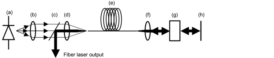
Figure 2. Q-switched fiber laser configuration.

Figure 3. Theoretical fluence (a) and pulse energy (b) of the designed ytterbium fiber laser.
The 304L stainless samples were obtained by cutting a bar into 1 mm disks using a computerized numerical control machine. The steel specimens were then sanded using ANSI/CAMI silicon carbide (SiC) papers with grit numbers of up to 1600, to make the surfaces smooth and uniform.
The alumina thin films were deposited by physical vapor deposition (PVD) on stainless steel substrate through unbalanced reactive magnetron sputtering using an Al target in mixed Ar and O2 atmosphere while employing a direct current power source. The deposition equipment and deposition process used have been described previously by Uribe et al. [20] prior to deposition, 304L substrate was polished to a mirror-like finish using a 6 mm diamond paste. The deposition run included two stages: in the first stage, a pure Aladhesion layer was deposited in a pure Ar atmosphere over a period of 5 min, while in the second stage, the oxide film was produced by the sputtering of the Al target in the Ar and O2 atmosphere. The films produced were of amorphous Al2O3 and had a fine columnar structure and a thickness of 800 nm to 1 mm. As can be observed in Figure 4, the thin film surface presents an homogenous structure with the presence of small cracks, typical of the PVD process.
3.2. Material Micromachining
The micromachining process was performed using a CO2 laser (wavelength of 10.6 µm). The parameters used were an average power of 18 W and spot diameter of 200 µm. These parameters were kept constant throughout the experiments, which consisted of machining lines with a length of 2 mm on each material at different scan rates, (24 - 4200 mm/min). Figure 5 shows the transversal micromachining depth profiles for 304L and Al2O3 for three different scan rates (24, 90, and 180 mm/min). As can be observed for both cases, it is clear that the micromachining process has been successfully achieved, and that the increment of the scan rate diminish the depth profile. As expected increasing scanning speed the ablation depth decreases due to reduced interaction time between laser and material, which generate a lower concentration of energy or fluence.
In the cases of 304L and the Al2O3 thin film, for scan rates greater than 350 mm/ min, ablation did not occur. Furthermore, there were areas where the laser beam did notcause ablation but the thin film showed fractures along the path over which the beamhad been scanned (Figure 6), presumably due to the thermal expansion with

Figure 4. Al2O3 thin film produced by PVD reactive magnetron sputtering.
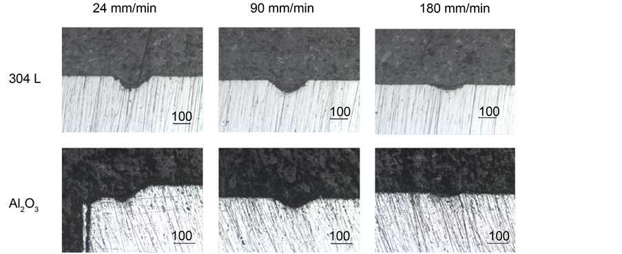
Figure 5. Transversal ablation profiles of 304L stainless steel and Al2O3.

Figure 6. Fractures generated in the Al2O3 thin film by the laser beam.
the heating process product of the interaction of the laser and the film, and the cooling when the laser is removed. This tends to produce a stress process on the surface leading to the fracture of the film. Furthermore it was observed that these cracks could contribute to the complete removal of the thin film, it can be observed that in the analyzed area. As can be observed the film was completely removed. The energy-dispersive X-ray spectroscopy (EDS) analysis (Figure 7) indicated that, in the area, the Al element was almost completely removed, and it has exposed the elements of the substrate material, as can be deduced elements present are those related with the 304L, insure the photomechanical ablation processes.
Finally, as it can be seen in Figure 8, silicon did not exhibit ablation at the lowest

Figure 7. Results of the EDS analysis of the Al2O3 thin film at 350 mm/min scan speed.

Figure 8. SEM image showing the melting of silicon when scanned using a laser with a power of 18 W at 24 mm/min.
scan rate (24 mm/min), as micromachining did not occur at a significant depth. As mentioned in Section 2.3 for a wavelength of 10.6 µm, the silicon absorption coefficient tends to be zero. It entails a high heat dissipation rate thus preventing the ablation process.
4. Conclusions
In this study, we determined the ablation thresholds for 304L, Al2O3, and silicon when scanned using a continuous-wave CO2 laser with a wavelength of 10.6 µm and average power of 18 W. In order to explore the photo-ablation process, the physical and optical properties of the materials, such as their extinction coefficients and refractive indices, were considered. Based on the design Q-switched ytterbium laser and the ablation experiments, the following are the main outcomes:
・ Laser micromachining with a continuous-wave CO2 laser can be used for micromachining conductive metals and oxides.
・ The material removal process involves different mechanisms such as ablation, melting, and vaporization. The machining mechanism is mainly based on direct melting/ ablation.
・ The properties of semiconductors make it necessary to use pulsed lasers such as the ytterbium fiber laser described, which was designed to work within the range of pulse energy and fluence values required to machine the mentioned materials.
・ The quantity of material removed by ablation is related to the laser operation mode and power. From this viewpoint, the use of the Q-switched laser was an appropriate choice, as a low frequency generates a high pulse power, which would increase the material removal rate.
・ The scan speed is an important parameter for causing ablation in the material and for manipulating the penetration depth.
The use of the fiber laser designed in this study as well as the appropriate values of parameters such as pulse energy, fluence and scan speed should aid the for the formation of complex shapes in similar materials by direct laser ablation.
Acknowledgements
All authors are grateful to ITESM-CEM, Instituto Politecnico Nacional-Centro de Investi- gacion e Innovacion Tecnologica CIITEC-IPN, SIP-IPN, ITESM-QRO, and CONACYT, all from Mexico.
Cite this paper
de la Rosa-Santana, G., Alvarez-Chavez, J.A., Morano-Okuno, H.R., Morales-Ramirez, A.J. and Uribe, E. (2016) Photomechanical Ablation of 304L Stainless Steel, Aluminum Oxide (Al2O3) Thin Film, and Pure Silicon. Optics and Photonics Journal, 6, 275-288. http://dx.doi.org/10.4236/opj.2016.610028
References
- 1. Leone, C. (2015) Experimental Investigation on Laser Milling of Aluminium Oxide Using a 30 W Q-Switched Yb:YAG Fiber Laser. Optics & Laser Technology, 76, 127-137.
http://dx.doi.org/10.1016/j.optlastec.2015.08.005 - 2. Patel, C. (1964) Continuous-Wave Laser Action on Vibrational Transitions of CO2. Physical Review, 136, 1187-1193.
http://dx.doi.org/10.1103/PhysRev.136.A1187 - 3. Boot, H. (1966) Micromachining with a Pulsed Gas Laser. Electronics Letters, 2, 1.
http://dx.doi.org/10.1049/el:19660001 - 4. Pröll, J. (2014) Laser-Printing and Femtosecond-Laser Structuring of LiMn2O4 Composite Cathodes for Li-Ion Microbatteries. Journal of Power Sources, 255, 116-124.
http://dx.doi.org/10.1016/j.jpowsour.2013.12.132 - 5. Li, Z. (2009) Analysis of Oxide Formation Induced by UV Laser Coloration of Stainless Steel. Applied Surface Science, 256, 1582-1588.
http://dx.doi.org/10.1016/j.apsusc.2009.09.025 - 6. Wautelet, M. (1990) Laser-Assisted Reaction of Metals with Oxygen. Applied Physics, 50, 131-139.
http://dx.doi.org/10.1007/BF00343408 - 7. Pacquentin, W. (2015) Effect of Microstructure and Chemical Composition on Localized Corrosion Resistance of a AISI 304L Stainless Steel after Nanopulsed-Laser Surface Melting. Applied Surface Science, 356, 561-573.
http://dx.doi.org/10.1016/j.apsusc.2015.08.015 - 8. Lawrence, S. (2013) Mechanical and Electromechanical Behavior of Oxide Coatings Grown on Stainless Steel 304L by Nanosecond Pulsed Laser Irradiation. Surface and Coatings Technology, 235, 860-866.
http://dx.doi.org/10.1016/j.surfcoat.2013.09.013 - 9. Hamadou, L. (2006) Influence of Oxidation Time on Semiconductive Behavior of Thermally Grown Oxide Films on AISI 304L. Applied Surface Science, 252, 4209-4217.
http://dx.doi.org/10.1016/j.apsusc.2005.06.036 - 10. Zhao, S. (2006) The Optical Properties of Sputtered Composite of Al-AIN. Solar Energy Materials and Solar Cells, 90, 1861-1874.
http://dx.doi.org/10.1016/j.solmat.2005.11.006 - 11. Zhao, Z. (2004) Optical Properties of Aluminium Oxide Thin Films Prepared at Room Temperature by Off-Plane Filtered Cathodic Vacuum Arc System. Thin Solid Films, 1, 14-19.
http://dx.doi.org/10.1016/j.tsf.2003.09.047 - 12. Zhao, Z. (2003) Structural Characteristics and Mechanical Properties of Aluminium Oxide Thin Films Prepared by Off-Plane Filtered Cathodic Vacuum Arc System. Surface and Coatings Technology, 167, 234-239.
http://dx.doi.org/10.1016/S0257-8972(02)00912-X - 13. Dill, K. (1990) Analysis of Crystalline Phase Aluminum Oxide Particles from Solid Propellant Exhausts. Journal of Propulsion and Power, 6, 668-671.
http://dx.doi.org/10.2514/3.23269 - 14. Panitchakana, H. (2012) Characterization of Aluminum Oxide Films Deposited on Al2O3-TiC by RF Diode Sputtering. Procedia Engineering, 32, 902-908.
http://dx.doi.org/10.1016/j.proeng.2012.02.030 - 15. Goetzberger, A. (1998) Crystalline Silicon Solar Cells. John Wiles & Sons, New York.
- 16. Taniguchi, T. (2016) Detection of Antibody-Antigen Reaction by Silicon Nitride Slot-Ring Biosensors Using Protein G. Optics Communications, 365, 16-23.
http://dx.doi.org/10.1016/j.optcom.2015.11.068 - 17. Lo, K.H. (2009) Recent Developments in Stainless Steels. Materials Science and Engineering, 69, 39-104.
http://dx.doi.org/10.1016/j.mser.2009.03.001 - 18. Aggen, S. (2005) Metals Handbook: Properties and Selection: Irons, Steels and High Performance Alloys. ASM International.
- 19. Mahrle, A. (2009) Theoretical Aspects of Fibre Laser Cutting. Journal of Physics D: Applied Physics, 42.
http://dx.doi.org/10.1088/0022-3727/42/17/175507 - 20. Hull, R. (1999) Properties of Crystalline Silicon. INSPEC, London.
- 21. Elwell, D. (1981) Electrowinning of Silicon from Solutions of Silica in Alkali Metal Fluoride/Alkaline Earth Fluoride Eutectics. Solar Energy Materials & Solar Cells, 5, 205-210.
http://dx.doi.org/10.1016/0165-1633(81)90032-0 - 22. Elwell, D. (1981) Electrocrystallization of Semiconducting Materials from Molten Salt and Organic Solutions. Journal of Crystal Growth, 52, 741-752.
http://dx.doi.org/10.1016/0022-0248(81)90371-7 - 23. Canovic, S. (2010) CVD TiC/Alumina and TiN/Alumina Multilayer Coatings Grown on Sapphire Single Crystals. International Journal of Refractory Metals and Hard Materials, 28, 163-173.
http://dx.doi.org/10.1016/j.ijrmhm.2009.08.001 - 24. Balakrishnan, G. (2010) Structural and Optical Properties of γ-Alumina Thin Films Prepared by Pulsed Laser Deposition. Thin Solid Films, 518, 3898-3902.
http://dx.doi.org/10.1016/j.tsf.2009.12.001 - 25. Edwards, D.F. and Ochoa, E. (1980) Infrared Refractive Index of Silicon. Applied Optics, 19, 4130-4131.
http://dx.doi.org/10.1364/AO.19.004130 - 26. Chandler-Horowitz, D. and Amirtharaj, P.M. (2005) High-Accuracy, Mid Infrared (450 cm-1 ≤ ω ≤ 4000 cm-1) Refractive Index Values of Silicon. Journal of Applied Physics, 97, Article ID: 123526.
- 27. Houska, J. (2012) Overview of Optical Properties of Al2O3 Films Prepared by Various Techniques. Thin Solid Films, 520, 5405-5408.
http://dx.doi.org/10.1016/j.tsf.2012.03.113 - 28. Aguilar-Morales, A. (2015) Photomechanical Ablation in Obsidianus Lapis via Q-Switched 1064-nm Laser Energy. Optical Engineering, 54, Article ID: 097101.
http://dx.doi.org/10.1117/1.oe.54.9.097101 - 29. Mohr, P.J. (2005) CODATA Recommended Values of the Fundamental Physical Constants. Reviews of Modern Physics, 77, 351-495.
http://dx.doi.org/10.1103/RevModPhys.77.1 - 30. Green, M.A. (2008) Self-Consistent Optical Parameters of Intrinsic Silicon at 300 K Including Temperature Coefficients. Solar Energy Materials & Solar Cells, 98, 1305-1310.
http://dx.doi.org/10.1016/j.solmat.2008.06.009 - 31. Hetch, J. (1993) Understanding LASERS an Entry-Level Guide. Board, New York.
- 32. Zhang, W. (2016) Fiber Laser Sensors for Micro Seismic Monitoring. Measurement, 79, 203-210.
http://dx.doi.org/10.1016/j.measurement.2015.09.046 - 33. Alvarez-Chavez, J.A. (2003) High-Power Fibre Lasers. PhD Thesis, University of Southampton, Southampton.
- 34. Ascari, A. (2014) Nanosecond Pulsed Laser Welding of High Carbon Steels. Optics & Laser Technology, 56, 25-34.
http://dx.doi.org/10.1016/j.optlastec.2013.07.016 - 35. Tao, S. (2012) Infrared Long Nanosecond Laser Pulse Ablation of Silicon: Integrated Two-Dimensional Modeling and Time-Resolved Experimental Study. Applied Surface Science, 258, 7766-7773.
http://dx.doi.org/10.1016/j.apsusc.2012.04.141 - 36. Sinha, S. (2015) Thermal Model for Nanosecond Laser Ablation of Alumina. Ceramics International, 41, 6596-6603.
http://dx.doi.org/10.1016/j.ceramint.2015.01.106 - 37. Csele, M. (2004) Fundamentals of Light Sources and Lasers. John Wiley & Sons Inc., Hoboken.
- 38. Dustin, G. and Roach, W. (2007) A Thermal Model of Laser Absorption. Conference on Optical Interactions with Tissue and Cells, 6435, 643506.