Paper Menu >>
Journal Menu >>
 J ournal o f Co m Published Onli n http://dx.doi.or g Open Access A Digi t Succes s Conve r Ling Du, Ni State Key Lab o China. Email: dulingst Received Octo b ABSTRA C A digital bac k p roximation r based on tri-l e erence capaci t To make a c o quantized twi c sion. The dif f calibration. T h b e estimated. ADC with 3 % (SNDR) is i m to 85.4 dB. Keywords: A 1. Introdu c As the dime n scale down, t h register analo prominent ov e structure. For tial building b comparator a with devices s recent years, r tensively rep o b rought dow n p rocess to d e Analog Con v match of suc h the linearity o match error i ADC if small domain back g analog-domai n mp uter and Co m n e November 2 0 g /10.4236/jcc.2 0 t al Bac k s ive A p r ter ng Ning, Sh u o f Electronic T h er@gmail.co m b e r 2013 C T k ground calib r r egister analo g e vel switchin g t or and the di g o mparison bet w c e. The unit c a f erence betwe e h e calibration Behavior si m % random cap a m proved from 5 A nalog-to-Digi t c tion n sion of CM O h e advantage s g-to-digital c o e r other ADC a charge redist r b locks, inclu d a nd digital ci r s caling down i r esearches on h o rted [1-5]. T n to the limit a l e crease the se t v erter (DAC) h small capa c o f the ADC. C i s indispensa b unit capacito r g round calibr a n calibration m munications, 2 0 13 (http://ww w 0 13.16006 k groun p proxi m u angyi Wu, h in Films and I n r ation techniq u g -to-digital co n g . The termina g ital weights o w een the size a pacitor bein g e n the two co n technique wit h m ulation is pe r a citor mismat c 5 7.2 dB to 72. 2 t al Conversio n O S technolo g s of successiv e o nverter (SA R architectures d r ibution SAR A d ing switched- r cuits, can be i nto the nano s h igh speed S A T he unit capa c l lowed by kT / t tling time o f [1-3,6,7]. Ho w c itors is sever e C alibration o f b le for high r r s are used. R a tion is more as the desig n 2 013, 1, 30-36 w .scirp.org/jour n d Cali b m ation R Qi Yu, Yan g n tegrated Devic e u e that correc t n verter (SAR tion capacitor f all other uni t of the unit ca p g calibrated is s n version result s h two referen c r formed to ve r c h. The simul a 2 dB and the S n ; Capacitor M g y continues t e approximati o R ADC) b eco m d ue to its simp A DC, the esse n capacitor arra well design e s cale domain. I A R ADC are e x c itor is usual l / C noise and t h f the Digital-t o w ever, the mi e , and degrad e f capacitor mi r esolution S A R ecently, digit a preferred th a n complexi t y n al / jcc) b ration R egiste r g Liu e s, University o f t s the capacito ADC). The t in the Digita l t capacitors ar e p acitor and t h a s wapped with s is used to c o c e capacitors i r ify the prop o a tion results s h purious Free D M ismatch; Digi t t o o n m e le n - a y, e d I n x - l y h e o - i s- e s s- A R a l- a n is transfe r device domai n p roces s In [ 8 ADC t o tical S A The di f the di g archite c and ar e b ackgr o SAR A two a n quanti z of eac h dynam i ditheri n MSB c signal weight Techn i r Anal o f Electronic Sci e r mismatches t echnique is i m l -to-Analog C o e corrected w i a t of the refer e the reference o rrect the digit a s presented to o sed calibratio n h ow that the S D ynamic Ran g t al Backgroun r red to digital scaling of C M n calibration tr s and environ m 8 ], the “split A o correct the c A R ADCs ar e f ference of th e g ital weights o c ture however e a of the an a o und digital c A DC quantizes n alog offsets. z ation results i h capacitor. In i c range is re d n g technique i apacito r weig h is injected to s are extract e i que fo r o g-to-D i e nce and Techn o error is prop o m plemented i n o nverter (DA C i th respect to t h e nce capacito r capacitor dur i a l weight of t h reduce the n u n technique b S ignal-to- N ois e g e (SFDR) is i m d Calibration; circuits whic h M OS technolo g acks the varia t m ental factors. A DC” architec t c apacitor mis m e used to qua n e ir output co d o f the capacit o , inevitably in c a log circuits. c alibration is each analog i The differe n s used to calc u this calibrati o d uced due to t i s developed i n h ts for the SA R the input si g e d from the r i gital o logy of China, o sed for succe s n SAR ADC w C ) is regarded h e reference c r , each input s i ng the secon d h e unit capaci t u mber of para m y using a 12- e and Distorti o m proved fro m SAR ADC h can benefit f g y. In addition t ions of the fa b t ure is applie d m atch error. T w n tize the inpu t d es is used to o rs. The “spl i c reases the co m A p erturbati o proposed in i nput signal t w n ce between u late the actu a o n algorithm, t t he offset inj e n [10] to exa m R ADC. The d g nal and the c dithered sig n JCC Chengdu, s sive ap- w hich is as a ref- apacitor. ample is d conver- t or under m eters to - bit SAR o n Ratio m 60.0 dB f rom the , digital- b rication d to SAR w o iden- t signals. estimate i t ADC” m plexity o n-based [9]. The w ice with the two a l weight t he input e ction. A m ine the d ithering c apacito r n al. The  A Digital Background Calibration Technique for Successive Approximation Register Analog-to-Digital Converter Open Access JCC 31 dithered signal is quantized twice to handle the problem of reduced signal range. However, an extra sample-and- hold amplifier, which holds the input signals for two ADC cycles, is needed for the calibration running in the background. This work presents a digital background calibration technique to correct the capacitor mismatch errors in SAR ADC with tri-level switching. Tri-level switching, which is widely used in SAR ADC [3,4,11], reduces the switching energy and the total capacitance [4]. In the proposed calibration technique, the termination capacitor in the DAC is regarded as a reference capacitor and the digital weights of all of other unit capacitors are cor- rected with respect to the reference capacitor. This paper is organized as follows. Section 2 intro- duces the tri-level switching method. Section 3 describes the details about the digital calibration technique. Beha- vior simulation results are presented in Section 4 and the conclusion is given in Section 5. 2. Tri-Level Switching Figure 1 shows the schematic of a 4-bit differential SAR ADC and its timing diagram. A 3-bit DAC can be used to realize a 4-bit SAR ADC based on the tri-level switching. Figure 2 shows the waveform of the reference voltage generated by the DAC and two different data formats. During the sampling phase, all the capacitors are con- nected to the input voltage and the top plates of the capa- citors are connected to VCM which equals to half of VREF. After that, all the capacitors are reset to VCM during the resetting phase. If VDAC,P > VDAC,N, C3,P is then switched from VCM to GND and C3,N is switched from VCM to VREF. All of the remaining capacitors are switched in the same manner. If the input voltage is Vi,1, the output code is “0110” according to each comparison result, as indicated in Figure 2. The output data format is offset binary. The output code can be derived in another way. The weights of the three capacitors in digital domain Wdi (i = 1, 2, and 3) are 00010, 00100 and 01000, respectively. The first bit of the digital weight is the sign bit. A 5-bit code is used to represent the digital weight of each capa- citor, which will be explained in the following para- graphs. If a capacitor is switched from VCM to VREF, the digital weight of the capacitor should be added to the output code; if a capacitor is switched from VCM to GND, the digital weight of the capacitor should be subtracted from the output code. In the above example, C3 is switched from VCM to GND while C2 and C1 are switch- ed from VCM to VREF. Therefore, the output code can be determined by Equation (1). The output data format is two’s complement. DOUT = −Wd3 + Wd2 + Wd1 = 11110 (1) (a) (b) Figure 1. (a) A 4-bit differential SAR ADC and (b) the timing diagram of the SAR ADC.  A Digital Background Calibration Technique for Successive Approximation Register Analog-to-Digital Converter Open Access JCC 32 Figure 2. The output data formats and the differential output voltage waveform of the DAC. The result of the last comparison, which is performed after the switching of C1, is useful. However, there is no capacitor that is switched after the switching of C1. The result given in Equation (1) cannot be taken directly as the final output code of the 4-bit SAR ADC. To solve this problem, a virtual capacitor CV is introduced with digital weight WdV = “00001”, which is half of the digi- tal weight of the LSB capacitor. If the last comparison indicates that VDACP > VDACN, the digital weight of the virtual capacitor should be subtracted from the output code, and vice versa. In the above example, if the input voltage is Vi,1, DOUT should be modified as DOUT = −Wd3 + Wd2 + Wd1 − WdV = 11101 (2) The higher 4-bit code, which is “1110”, is reserved as the final output code. If the input voltage is Vi,2, the last comparison would indicate that VDAC,P < VDAC,N, thus DOUT = −Wd3 + Wd2 + Wd1 + WdV = 11111. The final output code is 1111, which is also correct. 3. Digital Background Calibration 3.1. Basic Principle The capacitor array of the DAC shown in Figure 1 in- cludes eight unit capacitors. The single-ended DAC is redrawn in Figure 3(a). The binary weighted capacitors C3, C2 and C1 are composed of Cu,j (j = 4, 5, 6, and 7), Cu,j (j = 2 and 3) and Cu,1, respectively. The initial digital weight of Cu,j (j = 0, 1, …, 7) are 00010. In this calibra- tion technique, the termination capacitor Cu,0 is consi- dered as a standard capacitor and it is the reference capa- citor during the calibration. The analog weights of other unit capacitors are compared with that of Cu,0. If Cu,j is larger than Cu,0, the digital weight of Cu,j should be in- creased, and vice versa. The digital weight of Cu,0 re- mains unchanged. To compare the analog weights of Cu,j and Cu,0, each input signal is quantized twice. Figure 4 presents the timing diagram. In the first conversion, the schematic of the DAC is shown in Figure 3(a). C3, C2 and C1 are switched sequentially. In the second conversion, Cu,0 replaces Cu,j and Cu,j acts as the new termination capaci- tor. The schematic of the DAC during the second con- version is shown in Figure 3(b) assuming that Cu,3 is compared with Cu,0. As a result, C2 is composed of Cu,0 and Cu,2 rather than Cu,3 and Cu,2. As shown in Figure 4, during the second conversion, the switching activities of Cu,0 and Cu,2 are triggered after the switching of C3 whe- reas Cu,3 keeps connecting to VCM. The output code DOUT of each conversion is calculated as following: M OUTu,ju,j VV j=0 D=dWd+dWd (3) where Wdu,j is the digital weight of Cu,j; du,j = 1 or −1 if Cu,j is switched from VCM to VREF or GND; du,j = 0 if Cu,j acts as the termination capacitor; dV = ±1 according to the last comparison result; and M is the total number of unit capacitors. The difference between the two conver- sion results, ΔDOUT, can be used to correct the digital weight of Cu,j. Two cases are considered in the following. Case 1: Cu,j is switched from VCM to VREF in the first conversion. In this case, if Cu,j is larger than Cu,0, the DAC output voltage during the first conversion would be larger than that during the second conversion after Cu,j or Cu,0 is switched. Therefore, the output code of the first conver- sion would be smaller than that of the second conversion, or ΔDOUT < 0. If Cu,j is smaller than Cu,0, the DAC output voltage during the first conversion would be smaller than that  A Digital Background Calibration Technique for Successive Approximation Register Analog-to-Digital Converter Open Access JCC 33 (a) (b) Figure 3. (a) A 4-bit differential SAR ADC and (b) the timing diagram of the SAR ADC. Figure 4. The timing diagram of the DAC shown in Figure 3 when Cu,3 is under calibration. during the second conversion after Cu,j or Cu,0 is switched. Therefore, the output code of the first conversion would be larger than that of the second conversion, or ΔDOUT > 0. In case 1, the LMS (Least Mean Square) update equa- tion that is used to correct the digital weight of Cu,j can be written as: Wdu,j [n+1] = Wdu,j [n] − μΔDOUT (4) where μ is the convergence coefficient and n denotes the number of corrections. According to Equation (4), if Cu,j is larger than Cu,0, Wdu,j is increased since ΔDOUT < 0; if Cu,j is smaller than Cu,0, Wdu,j is decreased since ΔDOUT > 0. Wdu,j is corrected in the right direction in both situa- tions. When the digital weights of all unit capacitors ap- proach their final values, ΔDOUT is driven towards zero and the calibration process converges. Case 2: Cu,j is switched from VCM to GND in the first conversion In this case, if Cu,j is larger than Cu,0, the DAC output voltage during the first conversion would be smaller than that during the second conversion after Cu,j or Cu,0 is switched. Therefore, the output code of the first conver- sion would be larger than that of the second conversion, or ΔDOUT > 0. If Cu,j is smaller than Cu,0, the DAC output voltage during the first conversion would be larger than that dur- ing the second conversion after Cu,j or Cu,0 is switched. Therefore, the output code of the first conversion would be smaller than that of the second conversion, or ΔDOUT < 0. In case 2, the LMS update equation that is used to correct the digital weight of Cu,j can be written as: Wdu,j [n+1] = Wdu,j [n] + μΔDOUT (5) Wdu,j is also corrected in the right direction according to Equation (5). To reduce the estimation error of Wdu,j, the internal code length of the digital weights must be long enough. The unit capacitors are calibrated from Cu,1 to Cu,M se- quentially. The calibration process restarts from Cu,1 after Cu,M has been calibrated. The average value of the two conversion results is the final output. 3.2. Calibration Technique with Two Reference Capacitors The number of unit capacitor increases exponentially as the resolution of SAR ADC increases. For a 10-bit SAR ADC based on tri-level switching, there are 512 unit ca- 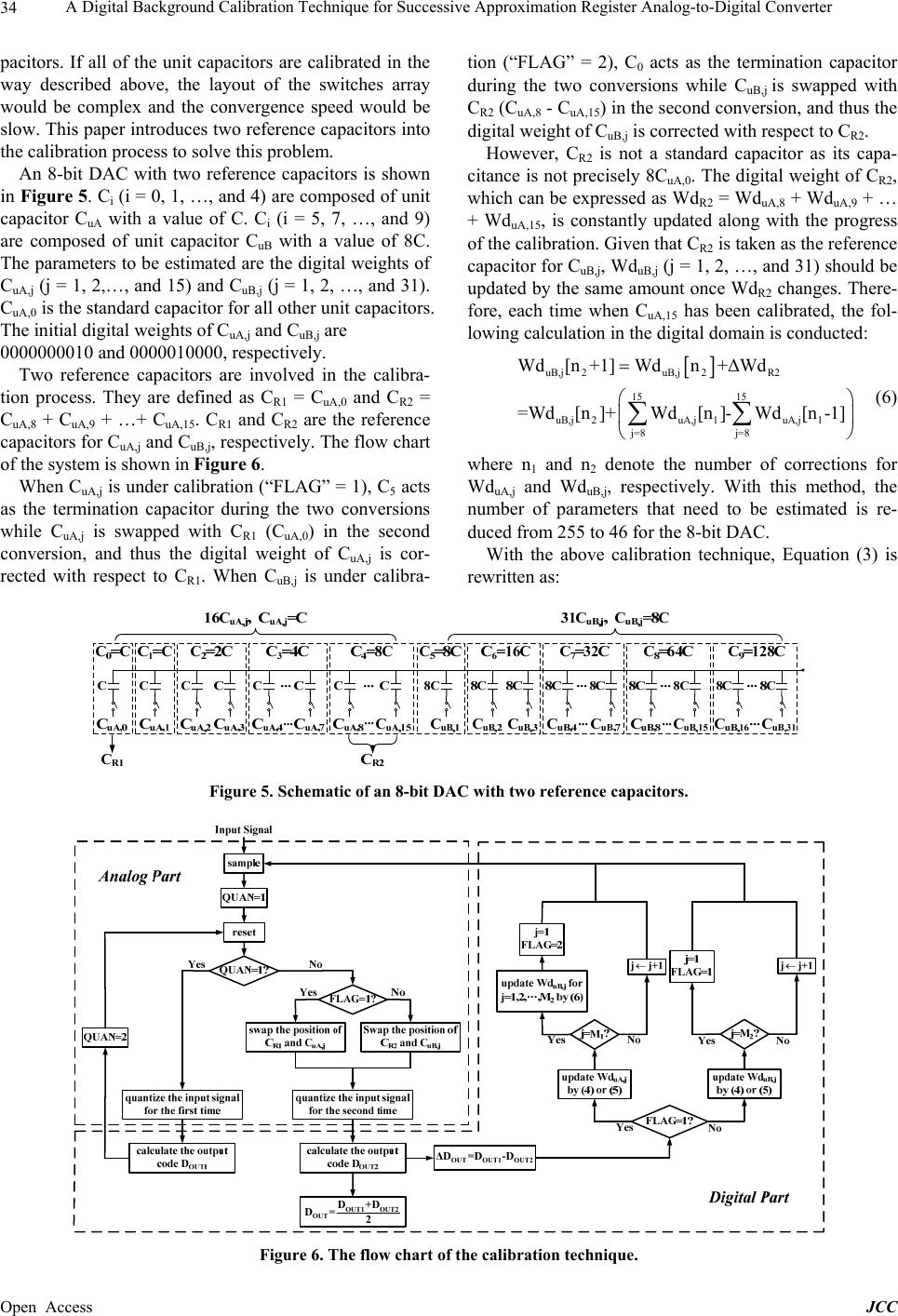 A Digital Background Calibration Technique for Successive Approximation Register Analog-to-Digital Converter Open Access JCC 34 pacitors. If all of the unit capacitors are calibrated in the way described above, the layout of the switches array would be complex and the convergence speed would be slow. This paper introduces two reference capacitors into the calibration process to solve this problem. An 8-bit DAC with two reference capacitors is shown in Figure 5. Ci (i = 0, 1, …, and 4) are composed of unit capacitor CuA with a value of C. Ci (i = 5, 7, …, and 9) are composed of unit capacitor CuB with a value of 8C. The parameters to be estimated are the digital weights of CuA,j (j = 1, 2,…, and 15) and CuB,j (j = 1, 2, …, and 31). CuA,0 is the standard capacitor for all other unit capacitors. The initial digital weights of CuA,j and CuB,j are 0000000010 and 0000010000, respectively. Two reference capacitors are involved in the calibra- tion process. They are defined as CR1 = CuA,0 and CR2 = CuA,8 + CuA,9 + …+ CuA,15. CR1 and CR2 are the reference capacitors for CuA,j and CuB,j, respectively. The flow chart of the system is shown in Figure 6. When CuA,j is under calibration (“FLAG” = 1), C5 acts as the termination capacitor during the two conversions while CuA,j is swapped with CR1 (CuA,0) in the second conversion, and thus the digital weight of CuA,j is cor- rected with respect to CR1. When CuB,j is under calibra- tion (“FLAG” = 2), C0 acts as the termination capacitor during the two conversions while CuB,j is swapped with CR2 (CuA,8 - CuA,15) in the second conversion, and thus the digital weight of CuB,j is corrected with respect to CR2. However, CR2 is not a standard capacitor as its capa- citance is not precisely 8CuA,0. The digital weight of CR2, which can be expressed as WdR2 = WduA,8 + WduA,9 + … + WduA,15, is constantly updated along with the progress of the calibration. Given that CR2 is taken as the reference capacitor for CuB,j, WduB,j (j = 1, 2, …, and 31) should be updated by the same amount once WdR2 changes. There- fore, each time when CuA,15 has been calibrated, the fol- lowing calculation in the digital domain is conducted: uB,j 2uB,j2R2 15 15 uB,j2uA,j 1uA,j 1 j=8 j=8 Wd[n +1]Wdn+ΔWd =Wd[n]+Wd[n]-Wd[n-1] (6) where n1 and n2 denote the number of corrections for WduA,j and WduB,j, respectively. With this method, the number of parameters that need to be estimated is re- duced from 255 to 46 for the 8-bit DAC. With the above calibration technique, Equation (3) is rewritten as: Figure 5. Schematic of an 8-bit DAC with two reference capacitors. OUTOUT1 OUT2 ΔD=D -D jj+1 OUT1 OUT2 OUT D+D D= 2 j j+1 Figure 6. The flow chart of the calibration technique.  A Digital Background Calibration Technique for Successive Approximation Register Analog-to-Digital Converter Open Access JCC 35 12 MM OUTuA,juA,j uB,juB,jVV j=0 j=1 D=dWd+dWd +dWd (7) 4. Simulation Results Behavior modeling and simulation has been performed with a 12-bit SAR ADC to verify the proposed calibra- tion technique. The system structure of a 12-bit SAR ADC is shown in Figure 7. The DAC is split into higher 8-bit sub-DAC and lower 3-bit sub-DAC to reduce the total capacitance. The higher 8-bit sub-DAC is the same as that shown in Figure 5 and the lower 3-bit sub-DAC is a binary weighted capacitor array. dL,j (j = 1, 2, and 3) are the bit decision results of the lower 3-bit. WdL,j (j = 1, 2, and 3) are the digital weights of the lower 3-bit and they are not updated. Mismatches of CS and the lower 3-bit capacitors do not deteriorate the ADC performance significantly. Random capacitor mismatches of 3% were added to all of the capacitors. The internal code length for the digital weights was 26-bit. The convergence coefficient μ was set to 2−12. The learning curve of the Signal-to-Noise and Distortion Ratio (SNDR) is shown in Figure 8. With calibration, the SNDR increases from 57.2 dB to 72.2 dB and the Spurious Free Dynamic Range (SFDR) increases from 60.0dB to 85.4dB. After about 700 000 samples, the SNDR converges to a stable value. The variations of WduA,1 and WduB,1, which are converted to decimal num- bers, are shown in Figure 9. The digital weights of all unit capacitors keep stable after they have converged. 5. Conclusion A digital background calibration technique for SAR ADC is proposed in this paper. Double conversions are carried out for each input sample. As the average value of the two conversion results is used as the final output, Figure 7. The system structure of a 12-bit SAR ADC. Figure 8. The learning curve of SNDR. Figure 9. The variations of WduA,1 and WduB,1. 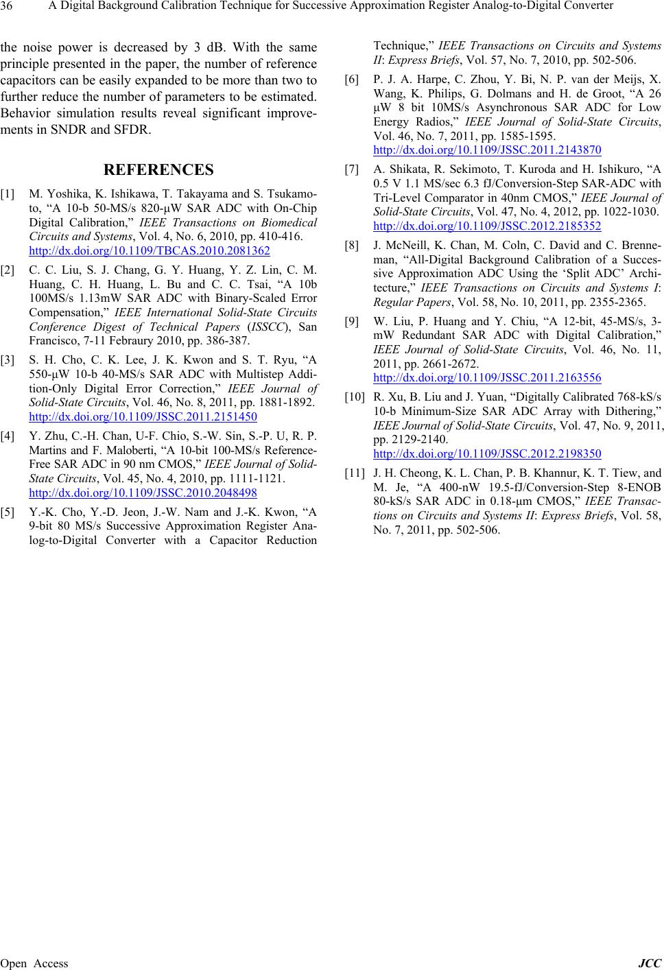 A Digital Background Calibration Technique for Successive Approximation Register Analog-to-Digital Converter Open Access JCC 36 the noise power is decreased by 3 dB. With the same principle presented in the paper, the number of reference capacitors can be easily expanded to be more than two to further reduce the number of parameters to be estimated. Behavior simulation results reveal significant improve- ments in SNDR and SFDR. REFERENCES [1] M. Yoshika, K. Ishikawa, T. Takayama and S. Tsukamo- to, “A 10-b 50-MS/s 820-μW SAR ADC with On-Chip Digital Calibration,” IEEE Transactions on Biomedical Circuits and Systems, Vol. 4, No. 6, 2010, pp. 410-416. http://dx.doi.org/10.1109/TBCAS.2010.2081362 [2] C. C. Liu, S. J. Chang, G. Y. Huang, Y. Z. Lin, C. M. Huang, C. H. Huang, L. Bu and C. C. Tsai, “A 10b 100MS/s 1.13mW SAR ADC with Binary-Scaled Error Compensation,” IEEE International Solid-State Circuits Conference Digest of Technical Papers (ISSCC), San Francisco, 7-11 Febraury 2010, pp. 386-387. [3] S. H. Cho, C. K. Lee, J. K. Kwon and S. T. Ryu, “A 550-μW 10-b 40-MS/s SAR ADC with Multistep Addi- tion-Only Digital Error Correction,” IEEE Journal of Solid-State Circuits, Vol. 46, No. 8, 2011, pp. 1881-1892. http://dx.doi.org/10.1109/JSSC.2011.2151450 [4] Y. Zhu, C.-H. Chan, U-F. Chio, S.-W. Sin, S.-P. U, R. P. Martins and F. Maloberti, “A 10-bit 100-MS/s Reference- Free SAR ADC in 90 nm CMOS,” IEEE Journal of Solid- State Circuits, Vol. 45, No. 4, 2010, pp. 1111-1121. http://dx.doi.org/10.1109/JSSC.2010.2048498 [5] Y.-K. Cho, Y.-D. Jeon, J.-W. Nam and J.-K. Kwon, “A 9-bit 80 MS/s Successive Approximation Register Ana- log-to-Digital Converter with a Capacitor Reduction Technique,” IEEE Transactions on Circuits and Systems II: Express Briefs, Vol. 57, No. 7, 2010, pp. 502-506. [6] P. J. A. Harpe, C. Zhou, Y. Bi, N. P. van der Meijs, X. Wang, K. Philips, G. Dolmans and H. de Groot, “A 26 μW 8 bit 10MS/s Asynchronous SAR ADC for Low Energy Radios,” IEEE Journal of Solid-State Circuits, Vol. 46, No. 7, 2011, pp. 1585-1595. http://dx.doi.org/10.1109/JSSC.2011.2143870 [7] A. Shikata, R. Sekimoto, T. Kuroda and H. Ishikuro, “A 0.5 V 1.1 MS/sec 6.3 fJ/Conversion-Step SAR-ADC with Tri-Level Comparator in 40nm CMOS,” IEEE Journal of Solid-State Circuits, Vol. 47, No. 4, 2012, pp. 1022-1030. http://dx.doi.org/10.1109/JSSC.2012.2185352 [8] J. McNeill, K. Chan, M. Coln, C. David and C. Brenne- man, “All-Digital Background Calibration of a Succes- sive Approximation ADC Using the ‘Split ADC’ Archi- tecture,” IEEE Transactions on Circuits and Systems I: Regular Papers, Vol. 58, No. 10, 2011, pp. 2355-2365. [9] W. Liu, P. Huang and Y. Chiu, “A 12-bit, 45-MS/s, 3- mW Redundant SAR ADC with Digital Calibration,” IEEE Journal of Solid-State Circuits, Vol. 46, No. 11, 2011, pp. 2661-2672. http://dx.doi.org/10.1109/JSSC.2011.2163556 [10] R. Xu, B. Liu and J. Yuan, “Digitally Calibrated 768-kS/s 10-b Minimum-Size SAR ADC Array with Dithering,” IEEE Journal of Soli d-State Ci rcuits, Vol. 47, No. 9, 2011, pp. 2129-2140. http://dx.doi.org/10.1109/JSSC.2012.2198350 [11] J. H. Cheong, K. L. Chan, P. B. Khannur, K. T. Tiew, and M. Je, “A 400-nW 19.5-fJ/Conversion-Step 8-ENOB 80-kS/s SAR ADC in 0.18-μm CMOS,” IEEE Transac- tions on Circuits and Systems II: Express Briefs, Vol. 58, No. 7, 2011, pp. 502-506. |