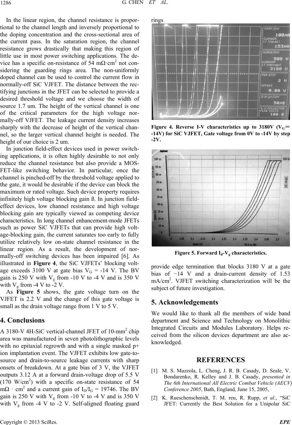
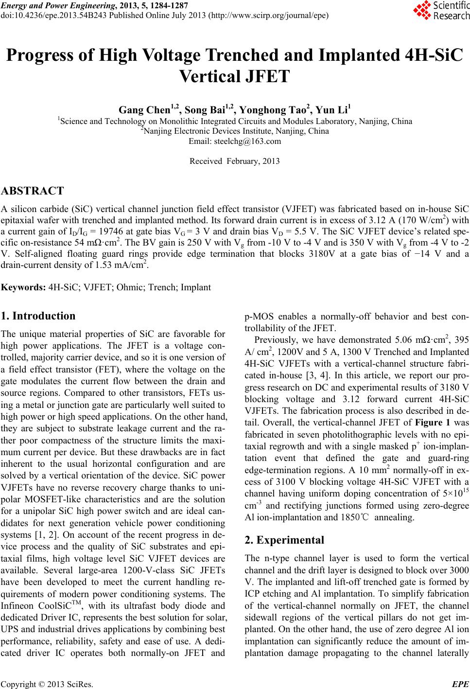
Energy and Power Engineering, 2013, 5, 1284-1287
doi:10.4236/epe.2013.54B243 Published Online July 2013 (http://www.scirp.org/journal/epe)
Progre ss of High Voltage Trenched and Implanted 4H-SiC
Vertical JFET
Gang Chen1,2, Song Bai1,2, Yonghong Tao2, Yun Li1
1Science and Technology on Monolithic Integrated Circuits and Modules Laboratory, Nanjing, China
2Nanjing Electronic Devices Institute, Nanjing, China
Email: steelchg@163.com
Received February, 2013
ABSTRACT
A silicon carbide (SiC) vertical channel junction field effect transistor (VJFET) was fabricated based on in-house SiC
epitaxial wafer with trenched and implanted method. Its forward drain current is in excess of 3.12 A (170 W/cm2) with
a current gain of ID/IG = 19746 at gate bias VG = 3 V and drain bias VD = 5.5 V. The SiC VJFET device’s related spe-
cific on-resistance 54 m·cm2. The BV gain is 250 V with Vg from -10 V to -4 V and is 350 V with Vg from -4 V to -2
V. Self-aligned floating guard rings provide edge termination that blocks 3180V at a gate bias of 14 V and a
drain-current density of 1.53 mA/cm2.
Keywords: 4H-SiC; VJFET; Ohmic; Trench; Implant
1. Introduction
The unique material properties of SiC are favorable for
high power applications. The JFET is a voltage con-
trolled, majority carrier device, and so it is one version of
a field effect transistor (FET), where the voltage on the
gate modulates the current flow between the drain and
source regions. Compared to other transistors, FETs us-
ing a metal or junction gate are particularly well suited to
high power or high speed applications. On the other hand,
they are subject to substrate leakage current and the ra-
ther poor compactness of the structure limits the maxi-
mum current per device. But these drawbacks are in fact
inherent to the usual horizontal configuration and are
solved by a vertical orientation of the device. SiC power
VJFETs have no reverse recovery charge thanks to uni-
polar MOSFET-like characteristics and are the solution
for a unipolar SiC high power switch and are ideal can-
didates for next generation vehicle power conditioning
systems [1, 2]. On account of the recent progress in de-
vice process and the quality of SiC substrates and epi-
taxial films, high voltage level SiC VJFET devices are
available. Several large-area 1200-V-class SiC JFETs
have been developed to meet the current handling re-
quirements of modern power conditioning systems. The
Infineon CoolSiCTM, with its ultrafast body diode and
dedicated Driver IC, represents the best solution for solar,
UPS and industrial drives applications by combining best
performance, reliability, safety and ease of use. A dedi-
cated driver IC operates both normally-on JFET and
p-MOS enables a normally-off behavior and best con-
trollability of the JFET.
Previously, we have demonstrated 5.06 m·cm2, 395
A/ cm2, 1200V and 5 A, 1300 V Trenched and Implanted
4H-SiC VJFETs with a vertical-channel structure fabri-
cated in-house [3, 4]. In this article, we report our pro-
gress research on DC and experimental results of 3180 V
blocking voltage and 3.12 forward current 4H-SiC
VJFETs. The fabrication process is also described in de-
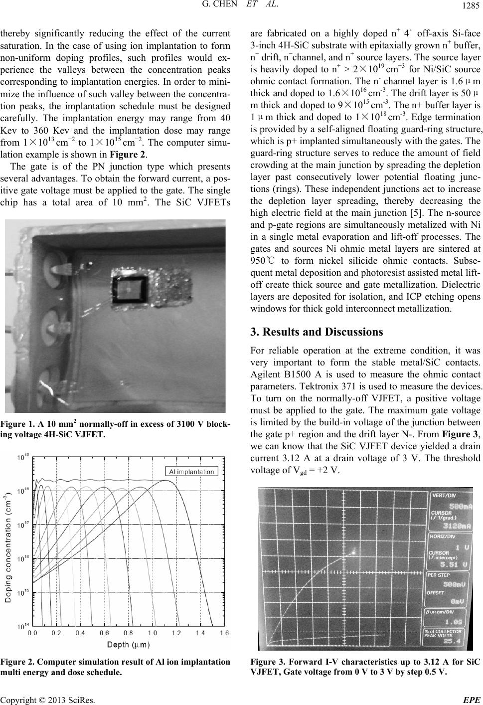
tail. Overall, the vertical-channel JFET of Figure 1 was
fabricated in seven photolithographic levels with no epi-
taxial regrowth and with a single masked p+ ion-implan-
tation event that defined the gate and guard-ring
edge-termination regions. A 10 mm2 normally-off in ex-
cess of 3100 V blocking voltage 4H-SiC VJFET with a
channel having uniform doping concentration of 5×10¹⁵
cm-3 and rectifying junctions formed using zero-degree
Al ion-implantation and 1850℃ annealing.
2. Experimental
The n-type channel layer is used to form the vertical
channel and the drift layer is designed to block over 3000
V. The implanted and lift-off trenched gate is formed by
ICP etching and Al implantation. To simplify fabrication
of the vertical-channel normally on JFET, the channel
sidewall regions of the vertical pillars do not get im-
planted. On the other hand, the use of zero degree Al ion
implantation can significantly reduce the amount of im-
plantation damage propagating to the channel laterally
Copyright © 2013 SciRes. EPE
G. CHEN ET AL. 1285
thereby significantly reducing the effect of the current
saturation. In the case of using ion implantation to form
non-uniform doping profiles, such profiles would ex-
perience the valleys between the concentration peaks
corresponding to implantation energies. In order to mini-
mize the influence of such valley between the concentra-
tion peaks, the implantation schedule must be designed
carefully. The implantation energy may range from 40
Kev to 360 Kev and the implantation dose may range
from 1×1013 cm2 to 1×1015 cm2. The computer simu-
lation example is shown in Figure 2.
The gate is of the PN junction type which presents
several advantages. To obtain the forward current, a pos-
itive gate voltage must be applied to the gate. The single
chip has a total area of 10 mm2. The SiC VJFETs
Figure 1. A 10 mm2 normally-off in excess of 3100 V block-
ing voltage 4H-SiC VJFET.
Figure 2. Computer simulation result of Al ion implantation
multi energy and dose schedule .
are fabricated on a highly doped n+ 4
off-axis Si-face
3-inch 4H-SiC substrate with epitaxially grown n+ buffer,
n drift, nchannel, and n+ source layers. The source layer
is heavily doped to n+ > 2×1019 cm3 for Ni/SiC source
ohmic contact formation. The n- channel layer is 1.6μm
thick and doped to 1.6×1016 cm-3. The drift layer is 50μ
m thick and doped to 9×1015 cm-3. The n+ buffer layer is
1μm thick and doped to 1×1018 cm-3. Edge termination
is provided by a self-aligned floating guard-ring structure,
which is p+ implanted simultaneously with the gates. The
guard-ring structure serves to reduce the amount of field
crowding at the main junction by spreading the depletion
layer past consecutively lower potential floating junc-
tions (rings). These independent junctions act to increase
the depletion layer spreading, thereby decreasing the
high electric field at the main junction [5]. The n-source
and p-gate regions are simultaneously metalized with Ni
in a single metal evaporation and lift-off processes. The
gates and sources Ni ohmic metal layers are sintered at
950 to form nickel silicide ohmic contacts. Subse-
quent metal deposition and photoresist assisted metal lift-
off create thick source and gate metallization. Dielectric
layers are deposited for isolation, and ICP etching opens
windows for thick gold interconnect metallization.
3. Results and Discussions
For reliable operation at the extreme condition, it was
very important to form the stable metal/SiC contacts.
Agilent B1500 A is used to measure the ohmic contact
parameters. Tektronix 371 is used to measure the devices.
To turn on the normally-off VJFET, a positive voltage
must be applied to the gate. The maximum gate voltage
is limited by the build-in voltage of the junction between
the gate p+ region and the drift layer N-. From Figure 3,
we can know that the SiC VJFET device yielded a drain
current 3.12 A at a drain voltage of 3 V. The threshold
voltage of Vgd = +2 V.
Figure 3. Forward I-V characteristics up to 3.12 A for SiC
VJFET, Gate voltage from 0 V to 3 V by step 0.5 V.
Copyright © 2013 SciRes. EPE
G. CHEN ET AL.
1286
In the linear region, the channel resistance is propor-
tional to the channel length and inversely proportional to
the doping concentration and the cross-sectional area of
the current pass. In the saturation region, the channel
resistance grows drastically that making this region of
little use in most power switching applications. The de-
vice has a specific on-resistance of 54 m·cm2 not con-
sidering the guarding rings area. The non-uniformly
doped channel can be used to control the current flow in
normally-off SiC VJFET. The distance between the rec-
tifying junctions in the JFET can be selected to provide a
desired threshold voltage and we choose the width of
source 1.7 um. The height of the vertical channel is one
of the critical parameters for the high voltage nor-
mally-off VJFET. The leakage current density increases
sharply with the decrease of height of the vertical chan-
nel, so the larger vertical channel height is needed. The
height of our choice is 2 um.
In junction field-effect devices used in power switch-
ing applications, it is often highly desirable to not only
reduce the channel resistance but also provide a MOS-
FET-like switching behavior. In particular, once the
channel is pinched-off by the threshold voltage applied to
the gate, it would be desirable if the device can block the
maximum or rated voltage. Such device property requires
infinitely high voltage blocking gain ß. In junction field-
effect devices, low channel resistance and high voltage
blocking gain are typically viewed as competing device
characteristics. In long channel enhancement-mode JFETs
such as power SiC VJFETs that can provide high volt-
age-blocking gain, the current saturates too early to fully
utilize relatively low on-state channel resistance in the
linear region. As a result, the development of nor-
mally-off switching devices has been impaired [6]. As
illustrated in Figure 4, the SiC VJFETs’ blocking volt-
age exceeds 3100 V at gate bias VG = -14 V. The BV
gain is 250 V with Vg from -10 V to -4 V and is 350 V
with Vg from -4 V to -2 V.
As Figure 5 shows, the gate voltage turn on the
VJFET is 2.2 V and the change of this gate voltage is
small as the drain voltage range from 1 V to 5 V.
4. Conclusions
A 3180-V 4H-SiC vertical-channel JFET of 10-mm2 chip
area was manufactured in seven photolithographic levels
with no epitaxial regrowth and with a single masked p+
ion implantation event. The VJFET exhibits low gate-to-
source and drain-to-source leakage currents with sharp
onsets of breakdown. At a gate bias of 3 V, the VJFET
outputs 3.12 A at a forward drain-voltage drop of 5.5 V
(170 W/cm2) with a specific on-state resistance of 54
m · cm2 and a current gain of ID/IG = 19746. The BV
gain is 250 V with Vg from -10 V to -4 V and is 350 V
with Vg from -4 V to -2 V. Self-aligned floating guard
rings
Figure 4. Reverse I-V characteristics up to 3180V (VG
-14V) for SiC VJFET, Gate voltage from 0V to -14V by step
-2V.
Figure 5. Forward Id-Vg characteristics.
provide edge termination that blocks 3180 V at a gate
bias of 14 V and a drain-current density of 1.53
mA/cm2. VJFET switching characterization will be the
subject of future investigation.
5. Acknowledgements
We would like to thank all the members of wide band
department and Science and Technology on Monolithic
Integrated Circuits and Modules Laboratory. Helps re-
ceived from the silicon devices department are also ac-
knowledged.
REFERENCES
[1] M. S. Mazzola, L. Cheng, J. R. B. Casady, D. Seale, V.
Bondarenko, R. Kelley and J. B. Casady, presented in
The 6th International All Electric Combat Vehicle (AECV)
Conference 2005, Bath, England, June 15, 2005,
[2] K. Rueschenschmidt, T. M. reu, R. Rupp, et al., “SiC
JFET: Currently the Best Solution for a Unipolar SiC
Copyright © 2013 SciRes. EPE
G. CHEN ET AL.
Copyright © 2013 SciRes. EPE
1287
High Power Switch,” Material Science Forum, Vol.
600-603, 2009, pp. 901-906.
doi:10.4028/www.scientific.net/MSF.600-603.901
[3] W. J. Ni, Y. Z. Li, Z. Y. Li, et al., “1200 V Normally-on
4H-SiC VJFET,” Research & Progress of Sse, Vol. 31,
No. 2, 2011, pp. 103-106.
[4] G. Chen, X. F. Song, S. Bai, et al.,5A 1300V Trenched
and Implanted 4H-SiC Vertical JFET,” Applied Mechan-
ics and Materials, Vol. 229-231, 2012, pp.
824-827.doi:10.4028/www.scientific.net/AMM.229-231.
824
[5] V. Veliadis, M. Snook, T. McNutt, H. Hearne, P. Potyraj,
A. Lelis and C. Scozzie,A 2055-V (at 0.7 mA/cm2)
24-A (at 706 W/cm2) Normally On 4H-SiC JFET With
6.8-mm2 Active Area and locking-Voltage Capability
Reaching the Material Limit,” IEEE Electronics Device
Letters, Vol. 29, No. 12, 2008, pp. 1325-1327.
[6] C. S. David and R. Andrew, “Semiconductor Devices
with Non-punch-through Semiconductor Channels Hav-
ing Enhanced Conduction and Methods of Making,” Pat-
ent No. US7994548 B2.