M. Saydé et al. / Journal of Biosciences and Medicines 1 (2013) 1-5
Copyright © 2013 SciRes. OPEN ACCESS
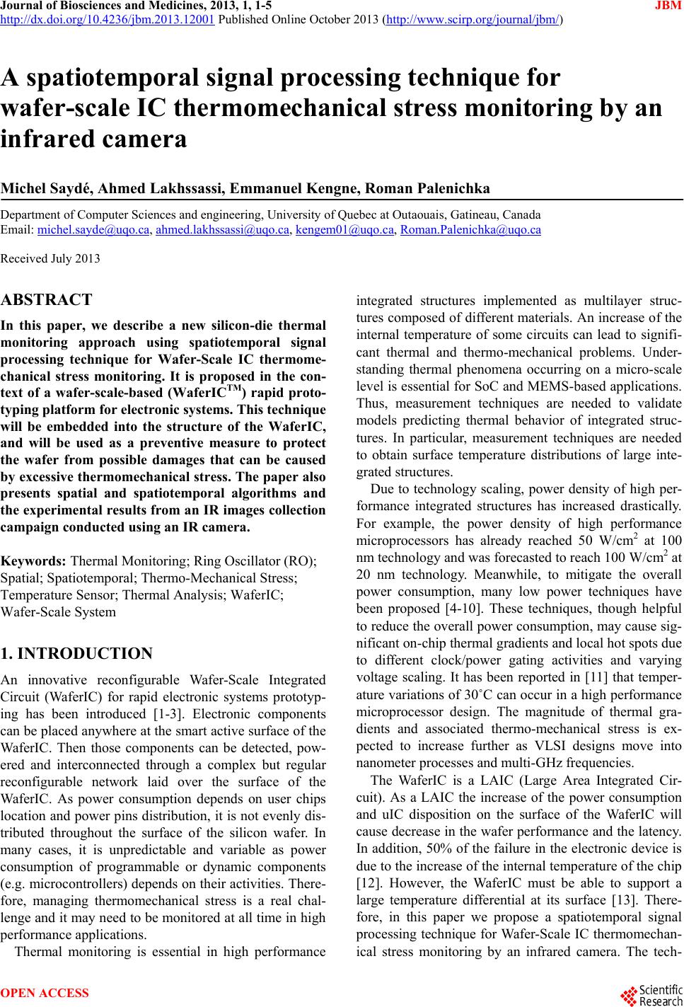
(a) (b)
Figure 5. Spatiotemporal derivative of Figure s 3(a) and (b)
give (a), then (b); and (c) give (b).
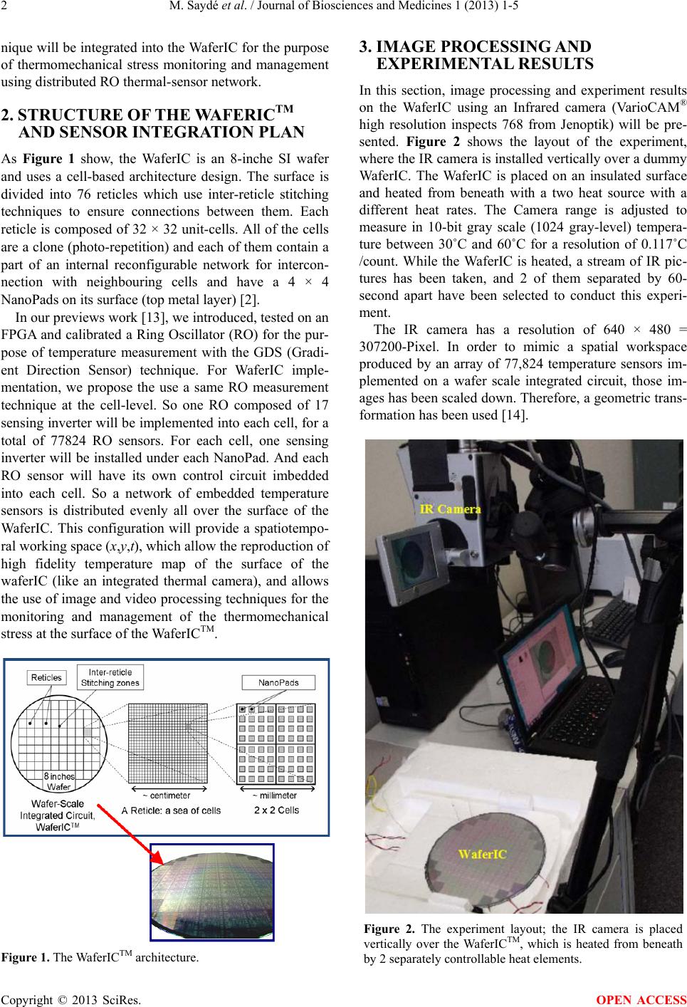
(a) (b) (c)
Figure 6. Isotherm map produced from images of Figure 3.
Then applying a median filter to produce homogenous
nn regions
(9)
Figure 6, show same images, thresholded with 16
gray-level, 7 × 7 bo x median filter is applied to generate
homogenous regions, then a Laplacien is used (which is
an isotropic second order derivative operator) to generate
a temperature isotherm map for each picture (from Fig-
ure 3). The variation of temperature from 30˚C to 60˚C
has been quantified into 16 levels (or isotherms). So each
level up represents a 1.875˚C temperature increase.
4. CONCLUSIONS
This paper has introduced a methodology to evaluate and
predict possible thermal stress in large VLSI circuits us-
ing an infrared camera. Important factors contributing to
LAIC circuit thermal heating were presented. The pro-
posed monitoring approach can be applied to produce a
thermal map of the surface of the WaferIC. Then a spatial
and spatiotemporal approach has been presented to ex-
tract from successive thermal images a relevant data
which will help to prevent thermomechanical stress from
damagi ng the WaferIC .
Results reported in this paper are encouraging and
provide a good insight into the issues that will be useful
to the process of defining an automated and embedded
method for detection and management of thermome-
chanical stress in LAICs circuit.
5. ACKNOWL EDG EMENTS
The authors thank the Natural Sciences and Engineering Research
Council of Canad a (NSERC), Le Regroupement Stratégiq ue en Micro-
systèmes du Québec (ReSMIQ) and CMC Microsystems for prov iding
design tools, support and associated technologies. The authors thank
the MITACS and Gestion TechnoCap Inc. for their financial support.
Finally, the authors thank prof. Mohand Said Allili for help with pro-
viding thermal camera.
REFERENCES
[1] Norman, R., Valorge, O., Blaquiere, Y., Lepercq, E.,
Basile-Bellavance, Y., El-Alaoui, Y., Prytula, R. and
Savaria, Y. (2008) An active reconfigurable circuit board.
2008 Joint 6th International IEEE Northeast Workshop
on Circuits and Systems and TAISA Conference, 351-354.
[2] Norman, R., Lepercq, E., Blaquiere, Y., Valorge, O.,
Basile-Bellavance, Y., Prytula, R. and Savaria, Y. (2008)
An interconnection network for a novel reconfigurable
circuit board. 2008 Joint 6th International IEEE North-
east Workshop on Circuits and Systems and TAISA Con-
ference, 129-132.
[3] Lepercq, E., Valorge, O., Basile-Bellavance, Y., Laflam-
me-Mayer, N., Blaquiere, Y. and Savaria, Y. (2009) An
interconnection network for a novel reconfigurable circuit
board. 2nd Microsystems and Nanoelectronics Research
Conference, 53-56.
[4] Sergent, J. and Krum, A. (1998) Thermal management
handbook for electronic assemblies. McGraw-Hill, New
York, Chapter 1, 1.1.
[5] Tze-chiang, C. (2006) Where CMOS is going: Trendy
hype vs. real technology. IEEE International Solid-State
Circuits Conference, Digest of Technical Papers, 1-18.
[6] Jaewon O. and Pedram, M. (2001) Gated clock routing
for low-power microprocessor design. IEEE Transactions
on Computer-Aided Design of Integrated Circuits and
Systems, 20, 715-722.
http://dx.doi.org/10.1109/43.924825
[7] Stok, L., Puri, R., Bhattacharya, S., Cohn, J., Sylvester,
D., Srivastava, A. and Kulkarni, S. (2007) Pushing ASIC
performance in a power envelope. Closing the Power
Gap between ASIC & Custom, Springer US, 323-356.
[8] Srivastava, A., Sylvester, D. and Blaauw, D. (2004) Con-
current sizing, Vdd and V<sub>th</sub> assignment for
low-power design. Proceedings of Desi gn, Automation
and Test in Europe Conference and Exhibition, 1, 718-
719.
[9] Kao, J., Chandrakasan, A. and Antoniadis, D. (1997)
Transistor sizing issues and tool for multi-threshold
CMOS technology. Proceedings of the 34th annual De-
sign Automation Conference, Anaheim, 409-414.
http://dx.doi.org/10.1109/DAC.1997.597182
[10] Changbo L. and Lei, H. (2004) Distributed sleep transis-
tor network for power reduction. IEEE Transactions on
Very Large Scale Integration (VLSI) Systems, 12, 937-
946.
[11] Gronowski, P. E., Bowhill, W.J., Preston, R.P., Gowan,
M.K. and Allmon, R.L. (1998) High-performance micro-
processor design. IEEE Journal of Solid-State Circuits,
33, 676-686.
http://dx.doi.org/10.1109/4.668981
[12] Yeh, L.T. (1995) Review of Heat Transfer Technologies
in Electronic Equipment. Journal of Electronic Packag-