K. B. TYNYSHTYKB AEV ET AL.
Copyright © 2013 SciRes. OPJ
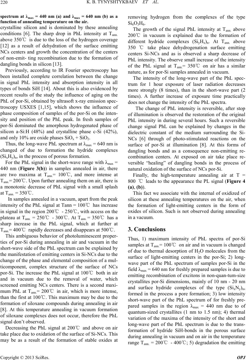
centers at Tann.> 400℃ and complete absence of PhL at
Tann.> 500℃ are observed due to the delete of hydride
SiH-bonds on the porous surface; 6) long excitation of
PL leads to heating that transforms of hydride complexes.
This fact confirms, that the light emitting centers are
formed due to hydride coverages of surface NCs por-Si;
7) a nnealing at Tann = 8 00℃ of por-Si on air leads to the
formation of light-emitting centers in the form of oxides
of silicon.
4. Acknowledgements
This work was supported financially by the Ministry of
Science and Education of Republic of Kazakhstan.
REFERENCES
[1] A. S. Lenshin, V. M. Kashkarov, S. Y. Turishchev, et al.,
“Influen ce of Natural Aging on the Photoluminescen ce o f
Porous Silicon,” Technica l Physics, Vol. 82, No. 2, 2012,
pp. 150–152.
[2] N. E. Korsunskaya, T. R. Stahr a, L. Y. Homenkova, et al.,
“Nature Emission of Porous Silicon Obtained by Chemi-
cal Etching,” Semiconductors, Vol. 44, No. 1, 2010, pp.
82-86. doi:10.1134/S1063782610010136
[3] K. B. Tynyshtykbaev, Y. A. Ryabikin, S. Z. Tokmoldin,
Т. Ajtmukan, B. A. Rakymeto v and R.B.Vermenichev,
“Morphology of Porous Silicon under Long Anodic
Etching in Electrolyte with Internal Current Source,”
Technical Physics Letters, Vol. 36, No 6, 2010, pp.
538-540.
[4] K. B. Tynyshtykbaev, Y. A. Ryabikin, K. A. Mit’, B. A.
Rakymetov, Т. Ajtmukan, “Dynamics of Formation of
Mosaic Structure of Porous Silicon at the Long-Term
Anode Etching in Electrolytes with Internal Current”.
Phys. Sol. State, Vol. 53, No. 8, 2011, pp. 1575-1580.
[5] K. B. Tynyshtykbaev, “Self-Organization of Highly Or-
dered Mosaic Structure of Porous Silicon at Long Anodic
Etching of P-Type Silicon in the Electrolyte with Internal
Current Source,” Proceedings of IEEE 2011, Vol. 7, pp.
6528-6531,2011.
[6] K. N. Yeltsov, V. A. Karavanskii, V. V. Martynov,
“Modifica t ion of Porous Silicon in Ultrahigh Vacuum and
the Contribution of Graphite Nanocrystallites Photolumi-
nescence,” JETP Lett., Vol. 63, No 2, 1996, pp. 106-111.
[7] V. A. Kiselev, S. V. Polisadin and A. V. Postnikov,
“Change the Optical Properties of Porous Silicon Due to
Thermal Annealing in A Vacuum,” Semiconductors, 1997,
Vol. 31, No. 7, pp. 830 -832. doi:10.1134/1.1187071
[8] B. M. Kostishko, I. P. Puzov and Ya. S. Nagornov, “Sta-
bilization of Light-Emitting Properties of Porous Silicon
Thermal Vacuum Annealing,” Technical Physics Letters,
Vol.26, No.1,2000, pp. 50-55. doi:10.1134/1.1262728
[9] B. M. Bulakh, N. E. Korsunskaya and L. Yu. Homenkova
et al., “The Effec t of Oxidation on the Efficienc y and the
Luminescence Spectrum of Porous Silicon,” Semicon-
ductors, Vol.40, No.5, 2006, pp. 614-620.
[10] T. P. Kolmakov, V. G. Baru, B. A. Malakho v et al.,
“Electro-and Photoluminescence in Thin Films of Porous
Silicon,” JETP Letters, Vol. 57, No. 7, 1993, pp.398-401.
[11] G. Polissky, O. M. Sreseli, A. V. Andrianov, F. Koch.
“Luminescence of Porous Silicon in the IR Spectrum at
Room Temperature,” Semiconductors, Vol.31, No 3,
1997, pp. 365- 369.
[12] P. K. Kashkarov, E. A. Konstantinova, S. A. Petrova, et
al., “On the Temperature Dependence of Photolumines-
cence of Porous Silicon,” Semiconductors, Vol . 31 , No. 6,
1997, pp.745-748. doi:10.1134/1.1187234
[13] N. E. Korsunskaya, T. B. Torchinsky, B. R. Dju maev, et
al., “Two Sources of Photoluminescence of Porous Sili-
con,” Semiconductors, Vol. 31 , No. 8, 1997, pp. 908-911.
doi:10.1134/1.1187246
[14] A. I. Belogorokhov, V. A. Karavanskii and L. I
Belogorokhov, “The Relationship Between th e Si gna l and
the Photoluminescence of Porous Silicon Surface States,
Including “free” of Porous Silicon,” Semiconductors, Vol.
30, No 7, 1999, pp. 1177-1185.
[15] A. S. Lenshin, V. M. Kashkarov, S . Ya. Turishchev, et al.,
“Influen ce of Natural Aging on the Photoluminescen ce o f
Porous Silicon,” Technical Physics Letters, Vol. 37,
No.17, 2011, pp. 1- 8.