L. X. ZOU ET AL. 67
enhanced chemical vapor deposition (PECVD) on the
laser wafe. Then, the microdisk patterns are transferred
onto the SiO2 layer using standard photolithography and
inductively coupled-plasma (ICP) etching techniques,
and the laser wafer is etched to about 4.7 μm using the
ICP technique subsequently with the patterned SiO2 layer
as hard mask. After the ICP etching process, a 200 nm
silicon nitride (SiNx) layer is deposited by PECVD on the
wafer to prepare a plane with better adhesion for the fol-
lowing DVS-BCB(divinyl siloxane bisbenzocyclobutene)
spin-coating process, and protect the cavities from the
following non-selective BCB etching process at the same
time. The DVS-BCB Cyclotene 3022-46 is coated twice
onto the wafer to create a planar cladding layer and then
experiences soft and hard cure in turn, and then the BCB
film is etched to expose the top of microdisk resonators
by Reactive Ion Etching (RIE) without any mask. After
that, a contact window is opened by ICP etching for cur-
rent injection on top of each resonator buried in BCB, on
which pad-patterned P-electrodes are formed afterward
using lifting off technology. Finally, the laser wafer is
mechanically lapped down to a thickness of about 120
μm, and an Au-Ge-Ni metallization layer is used as n-
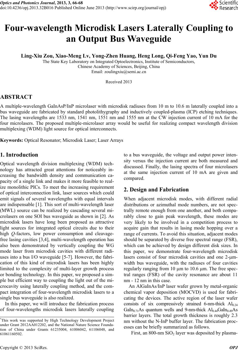
type patterned electrode. The microscopic pictures of
fabricated microdisk resonator microlasers with different
radiuses and a bus waveguide are shown in Figure 1,
where the circle patterns on the top of the resonators are
the etched current injection windows. The radiuses for
lasers 1 - 4 are 10.6 μm, 10.2 μm, 10.4 μm and 10 μm,
respectively.
3. Results and Discussion
The fabricated multi-wavelength MDL is bonded onto a
Cu heat sink and tested at room temperature without
temperature control. Metal needles are utilized to inject
continuous wave (CW) current onto each electrode pad
of the device, while a tapered fiber fixed at a three-di-
mensional stage is used to couple light out of the output
waveguide.
For MDLs with radiuses of 10 μm, 10.2 μm, 10.4 μm
and 10.6 μm, the lasing modes are coupled out using a
2-μm- width bus waveguide and collected by a tapered
multi- mode fiber. As shown in Figure 1, the bus
waveguide is tilted by 7°to avoid the Fabry-perot mode
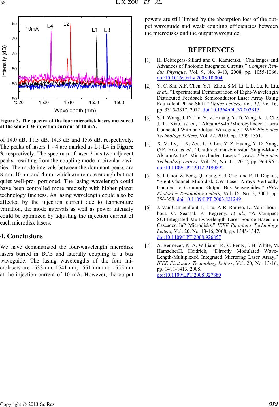
oscillation. The applied voltage and the output power
versus the CW injection current of laser 1 is shown in
Figure 2. By fitting this V-I curve, we get a series resis-
tance of 16 Ω. The output intensity of laser 1 is also
given and several kinks could be found in the L-I curves,
the first of which indicate the threshold current while the
others could be explained by the mode-jumping. The
threshold current at room temperature is about 3 mA es-
timated from the intersect point at the current axis for the
extended line of the output power curve as shown by the
dashed line in Figure 2. The maximum output powers of
the four microdisk lasers are 0.67 μW, 1.92 μW, 1.09 μW
and 3.89 μW for lasers 1 - 4, respectively. This power
diversity could be explained by the absorption effect of
bus waveguide, as it has the same quantum well struc-
tures with the microdisk cavity, thus microdisk lasers
locating further to the output facet would suffer more
absorption. Besides, the output power could also be op-
timized by improve the coupling efficiency between the
waveguide and microdisk cavities. But it is still chal-
lenging to solve those problems by conventional planar
process technology.
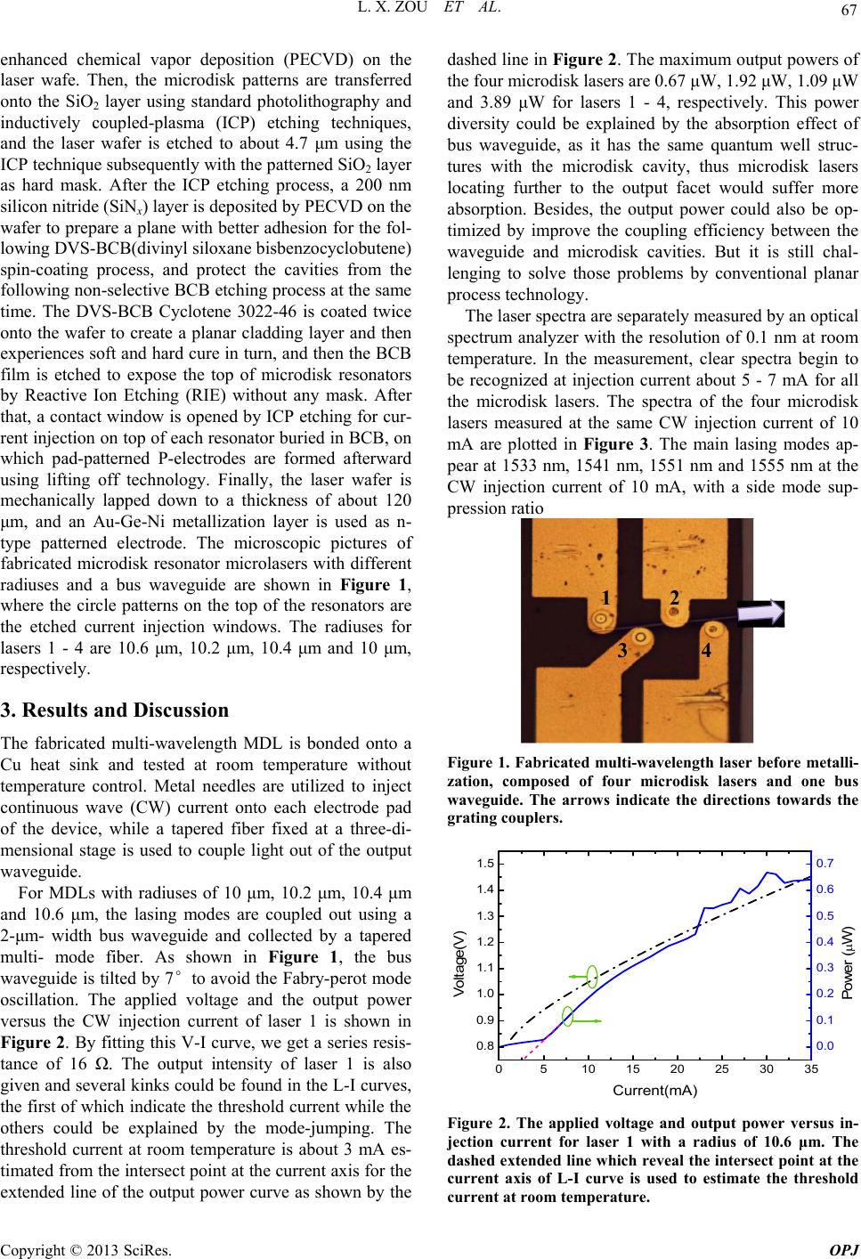
The laser spectra are separately measured by an optical
spectrum analyzer with the resolution of 0.1 nm at room
temperature. In the measurement, clear spectra begin to
be recognized at injection current about 5 - 7 mA for all
the microdisk lasers. The spectra of the four microdisk
lasers measured at the same CW injection current of 10
mA are plotted in Figure 3. The main lasing modes ap-
pear at 1533 nm, 1541 nm, 1551 nm and 1555 nm at the
CW injection current of 10 mA, with a side mode sup-
pression ratio
12
34
Figure 1. Fabricated multi-wavelength laser before metalli-
zation, composed of four microdisk lasers and one bus
waveguide. The arrows indicate the directions towards the
grating couplers.
0510 15 20 25 30 35
0.8
0.9
1.0
1.1
1.2
1.3
1.4
1.5
Current(mA)
Voltage(V)
0.0
0.1
0.2
0.3
0.4
0.5
0.6
0.7
Power (
W)
Figure 2. The applied voltage and output power versus in-
jection current for laser 1 with a radius of 10.6 μm. The
dashed extended line which reveal the intersect point at the
current axis of L-I curve is used to estimate the threshold
current at room temperature.
Copyright © 2013 SciRes. OPJ