Paper Menu >>
Journal Menu >>
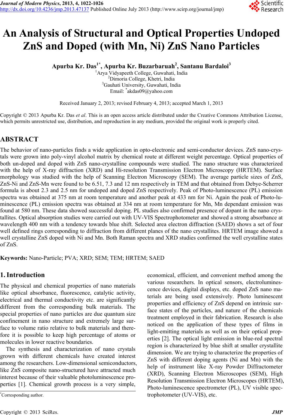 Journal of Modern Physics, 2013, 4, 1022-1026 http://dx.doi.org/10.4236/jmp.2013.47137 Published Online July 2013 (http://www.scirp.org/journal/jmp) An Analysis of Structural and Optical Prop erties Undoped ZnS and Doped (with Mn, Ni) ZnS Nano Particles Apurba Kr. Das1*, Apurba Kr. Buzarbaruah2, Santanu Bardaloi3 1Arya Vidyapeeth College, Guwahati, India 2Dimoria College, Khetri, India 3Gauhati University, Guwahati, India Email: *akdas09@yahoo.com Received January 2, 2013; revised February 4, 2013; accepted March 1, 2013 Copyright © 2013 Apurba Kr. Das et al. This is an open access article distributed under the Creative Commons Attribution License, which permits unrestricted use, distribution, and reproduction in any medium, provided the original work is properly cited. ABSTRACT The behavior of nano-particles finds a wide application in opto-electronic and semi-conductor devices. ZnS nano-crys- tals were grown into poly-vinyl alcohol matrix by chemical route at different weight percentage. Optical properties of both un-doped and doped with ZnS nano-crystalline compounds were studied. The nano structure was characterized with the help of X-ray diffraction (XRD) and Hi-resolution Transmission Electron Microscopy (HRTEM). Surface morphology was studied with the help of Scanning Electron Microscopy (SEM). The average particle sizes of ZnS, ZnS-Ni and ZnS-Mn were found to be 6.51, 7.3 and 12 nm respectively in TEM and that obtained from Debye-Scherrer formula is about 2.3 and 2.5 nm for undoped and doped ZnS respectively. Peak of Photo-luminescence (PL) emission spectra was obtained at 375 nm at room temperature and another peak at 433 nm for Ni. Again the peak of Photo-lu- minescence (PL) emission spectra was obtained at 334 nm at room temperature for Mn, Mn dependant emission was found at 580 nm. These data showed successful doping. PL studies also confirmed presence of dopant in the nano crys- tallites. Optical absorption studies were carried out with UV-VIS Spectrophotometer and showed a strong absorbance at wavelength 400 nm with a tendency towards blue shift. Selected area electron diffraction (SAED) shows a set of four well defined rings corresponding to diffraction from different planes of the nano crystallites. HRTEM image showed a well crystalline ZnS doped with Ni and Mn. Both Raman spectra and XRD studies confirmed the well crystalline states of ZnS. Keywords: Nano-Particle; PVA; XRD; SEM; TEM; HRTEM; SAED 1. Introduction The physical and chemical properties of nano materials like optical absorbance, fluorescence, catalytic activity, electrical and thermal conductivity etc. are significantly different from the corresponding bulk materials. The special properties of nano particles are due quantum size confinement in nano structure and extremely large sur- face to volume ratio relative to bulk materials and there- fore it is possible to keep high percentage of atoms or molecules in lower reactive boundaries. The synthesis and characterization of nano crystals grown with different chemicals have created interest among the researchers. Low-dimensional semiconductors, like ZnS composite nano-structured have attracted much interest because of their valuable photoluminescence pro- perties [1]. Chemical growth process is a very simple, economical, efficient, and convenient method among the various researchers. In optical sensors, electrolumines- cence devices, digital displays, etc. doped ZnS nano ma- terials are being used extensively. Photo luminescent properties and efficiency of ZnS depend on intrinsic sur- face states of the particles, and nature of the chemicals treatment employed in their fabrication. Research is also noticed on the application of these types of films in light-emitting materials as well as on their optical prop- erties [2]. The optical light emission in blue-red spectral region is characterized by blue shift at smaller crystallite dimension. We are trying to characterize the properties of ZnS with different doping agents (Ni and Mn) with the help of instrument like X-ray Powder Diffractometer (XRD), Scanning Electron Microscopes (SEM), High Resolution Transmission Electron Microscopes (HRTEM), Photo-luminescence spectrometer (PL), UV visible spec- trophotometer (UV-VIS), etc. *Corresponding author. C opyright © 2013 SciRes. JMP  A. K. DAS ET AL. 1023 Experimental The synthesisation ZnS nano-particles were done by using Polyvinyl Alcohol (PVA) as a matrix. Different weight% solutions of PVA and ZnCl2 in deion- ized water were taken and stirred at 200 rpm in a mag- netic stirrer at temperature 70˚C for 3 hours. The solution was kept overnight for complete dissolution and found to be transparent. A 2 weight% Na2S solution was added till the whole solution appears milky. The solution was kept over night inside a dark chamber. As soon as the nano- structure formed, it embedded into the gap. The chemical reaction took place as follows 22 ZnClNa SZnS 2NaCl To make different % of ZnS:Ni solution, NiCl2·6H2O was mixed by weight% with deionized water. Solution so obtained was mixed with another solution of PVA and ZnCl2. Then the solution was stirred at 200 rpm in a magnetic stirred at constant temperature 70˚C. 0.08 M weight% Na2S solution was added to the solution. Pre- cipitation found was washed with deionized water and taken for study. To make different % of ZnS:Mn solution, MnCl2·4H2O was mixed by weight% with deionized water. Solution so obtained was mixed with another solution of PVA and ZnCl2. Then the solution was stirred at 200 rpm in a magnetic stirrer at constant temperature 70˚C. 0.08 M weight% Na2S solution was added to the solution. Pre- cipitation found was washed with deionized water and taken for study. 2. Microstructure Studies 2.1. XRD Studies The XRD studies shown in Figures 1(a) and (b) were ob- tained from powder. Diffractogram was obtained from a Philips X’pert Pro Powder diffractometer using Cu Kα radiation with the operating voltage 40 kV and current 20 mA. The pattern observed was found to be within the nano range [3,4]. XRD patterns revealed the films to be polycrystalline [5]. Planes (111), (220) and (311) were found to present which tallied well with the JCPDS card No. 05-0566. The average particle size corresponding to the FWHM was calculated with the Scherrer formulae 12 0.94 cos Dp in case of undoped ZnS, which is also in good agree- 0 1020304050607080 0 10 20 30 40 50 60 70 and found to be 2.3 nm [6]. 2.2. Electron Diffraction Studies Selected area electron diffraction (SAED) was done with the help of HRTEM. Photo of SAED of undoped ZnS (Figures 2(a)-(c)) also showed a set of three well defined rings corresponding to the planes (111), (220) and (311) 80 (o %) (311) (220) (111) Intensity 2 (in Degrees) (a) 0 102030405060708090100 0 1000 2000 3000 4000 5000 Int e ns ity Wave length in nm 1% Mn 1% Ni (b) Figure 1. (a) XRD diffractogram of ZnS; (b) XRD diffrac- togram of ZnS-Mn. (a) (b) (c) Figure 2. (a) SAED of ZnS; SAED of ZnS-Ni; (c) SAED of ZnS-Mn. (b) Copyright © 2013 SciRes. JMP  A. K. DAS ET AL. 1024 ment with that of XRD data. 2.3. SEM Studies Photographs of the nano-crystalline thin film were taken crystalline doped ptical Absorbance Study f ZnS was recorded with (JEOL, JSM-6360) SEM and shown in Figure 3. The surface morphology of the film prepared at 70˚C with PVA was observed and found that all the particles formed not exactly spherical. Study showed that the sur- face of the film was smooth, uniform and without any crack. The particle sizes of ZnS-Ni, ZnS-Mn were found to be 7 - 16 and 7 - 15 nm respectively. 2.4. Photo Luminescence Studies The photo luminescence studies of nano & un-doped (Figure 4) were done at room temperature by using F-2500 FL Spectrophotometer. In all the meas- urement the excitation wavelength was 240 nm. Emis- sion spectra showed a broad peak at 378 nm and another small broad peak at 451 nm for ZnS while 375 nm and 433 nm for ZnZ-Ni (0.5%) and at 382 nm for ZnS-Ni. For Mn the emission spectra showed a broad peak at 346 nm and another small broad peak at 468 nm. PL in this region is due to the presence of S vacancies in the lattice. PL spectra of ZnS:Mn thin film revealed yellow-orange emissions. Mn dependent yellow emission was found at 580 nm which was also a confirmation successful Mn doping. Starting with the blue emission (at 468 nm), in- tensity decreases towards the orange emission (at 580 nm) [7]. PL spectra of ZnS:Ni revealed yellow-orange emis- sions. 2.5. O The optical absorbance (Figure 5) o at room temperature using a Double Beam Automated Spectrophotometer (Hitachi-U3210) where the meas- urement of optical absorbance was done in the range 200 - 800 nm. The wavelength showed strong absorption. The peak of the absorption showed at 287 nm for ZnS. The peak of the absorption showed blue shift with re- spect to bulk attributing quantum confinement effect on the nano-particles. Optical absorption studies were car- ried out with UV-VIS Spectrophotometer and showed a (a) (b) Figure 3. (a) SEMb) SEM micr graph of ZnS-Mn 200 300 400 500 600 700 800 -100 0 100 200 300 400 500 600 700 micrograph of ZnS-Ni; ( . o- 800 Intensity Wave length in nm 0% 0.5% Ni 1% Ni (a) (b) Figure 4. (a) PL spectra of Z, ZnS-Ni; (b) PL spectra of Zn-S, ZnS-Mn. ce at wavelength 400 nm with a tendency shows clear lattice fringes of the (001) peak of Raman spectra indicated −1 n-S strong absorban towards blue shift. Optical absorbance spectrum of ZnS-Ni (0.5%, 1.0%) features a strong peak around 400 nm. This spectra of undoped and Ni doped ZnS nano crystal are distinguish- able. This indicates that Ni doping has effect on the elec- tronic absorption spectra of ZnS [8]. This may be possi- ble for low doping level. 2.6. HRTEM HRTEM image plane indicating crystal growth along (001) direction. The particle size obtained from HRTEM image is 6 nm and 7.3 nm for ZnS-Ni and ZnS-Mn respectively. 2.7. Raman Studies In Figure 6 the sharp ZnS in well crystalline state. The peaks at 58 cm and 335 cm−1, 347 cm−1 are the characteristic Raman scatter- ing of ZnS and indexed to LO phonon mode [9]. Another Copyright © 2013 SciRes. JMP  A. K. DAS ET AL. Copyright © 2013 SciRes. JMP 1025 3.0 200 300 400 500 0.0 0.5 1.0 1.5 2.0 2.5 600 700 Absorbance (a.U) Wave length in nm 0% 600 400 450 500 550 0.05 0.10 0.15 0.20 0.25 0.30 0.35 0.40 0.45 Absorbance (a.u.) Wave length in nm 0.5% Ni 1% (b) Ni (a) 700 800200 300 400 500 600 0.0 0.5 1.0 1.5 2.0 2.5 Absorbance (a. U) Wave length in nm 0.5% Mn 1% Mn (c) Figure 5. (a) Absorbance spectra of ZnS; (b) Absorbanpectra of ZnS-Ni; (c) Absorbce spectra of ZnS-Mn. ce san Figure 6. Raman spectra. 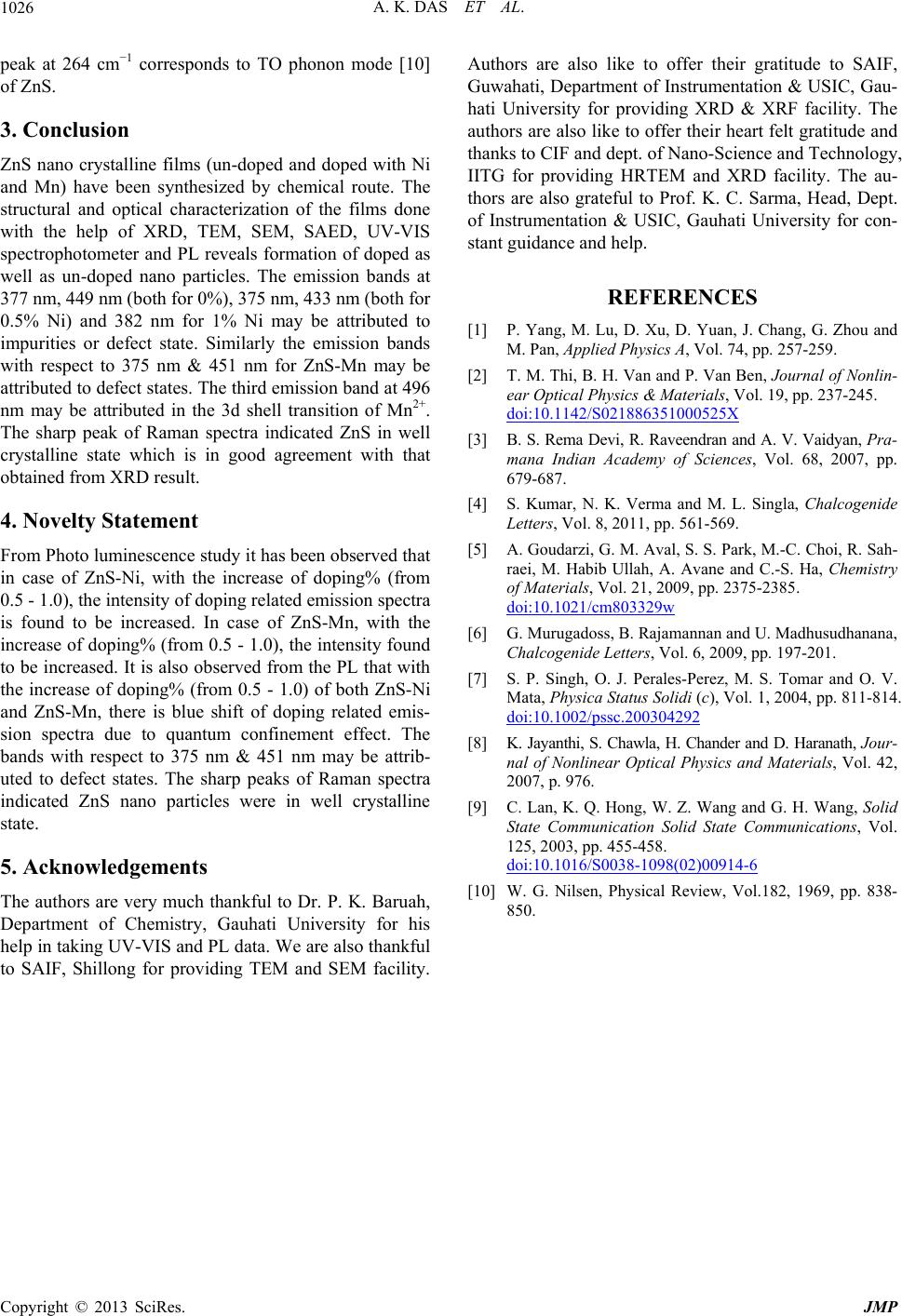 A. K. DAS ET AL. 1026 peak at 264 cm−1 corresponds to TO phonon mode [10] of ZnS. 3. Conclusion ZnS nano crystalline films (un-doped and doped with Ni and Mn) have been synthesized by chemical route. The structural and optical characterization of the films done with the help of XRD, TEM, SEM, SAED, UV-VIS spectrophotometer and PL reveals formation of doped as well as un-doped nano particles. The emission bands at 377 nm, 449 nm (both for 0%), 375 nm, 433 nm (both for 0.5% Ni) and 382 nm for 1% Ni may be attributed to impurities or defect state. Similarly the emission bands with respect to 375 nm & 451 nm for ZnS-Mn may be attributed to defect states. The third emission band at 496 nm may be attributed in the 3d shell transition of Mn2+. The sharp peak of Raman spectra indicated ZnS in well crystalline state which is in good agreement with that obtained from XRD result. From Photo luminescence study it has been observed that , with the increase of doping% (from Gauhati University for his help in taking UV-VIS and PL data. We are also tha g TEM and SEM facility. Authors are also like to offer their gratitude to SAIF, Guwahati, Department of Instrumentation & USIC, Gau- hati University for providing XRD & XRF facility. The authors are also like to offer their heart felt gratitude and thanks to CIF and dept. of Nano-Science and Technology, IITG for providing HRTEM and XRD facility. The au- thors are also grateful to Prof. K. C. Sarma, Head, Dept. of Instrumentation & USIC, Gauhati University for con- stant guidance and help. REFERENCES [1] P. Yang, M. Lu, D. Xu, D. Yuan, J. Chang, G. Zhou and M. Pan, Applied Physics A, Vol. 74, pp. 257-259. [2] T. M. Thi, B. H. Van and P. Van Ben, Journal of Nonlin- ear Optical Physics & Materials, Vol. 19, pp. 237-245. doi:10.1142/S021886351000525X [3] B. S. Rema Devi, R. Raveendran and A. V. Vaidyan, Pra- mana Indian Academy of Sciences, Vol. 68, 2007, pp. 7. . Kumar, N. K. Verma and M. L. Singla, Chalcogenide etters, Vol. 8, 2011, pp. 561-569. S. S. Park, M.-C. Choi, R. Sah- vane and C.-S. Ha, Chemistry 4. Novelty Statement in case of ZnS-Ni 0.5 - 1.0), the intensity of doping related emission spectra is found to be increased. In case of ZnS-Mn, with the increase of doping% (from 0.5 - 1.0), the intensity found to be increased. It is also observed from the PL that with the increase of doping% (from 0.5 - 1.0) of both ZnS-Ni and ZnS-Mn, there is blue shift of doping related emis- sion spectra due to quantum confinement effect. The bands with respect to 375 nm & 451 nm may be attrib- uted to defect states. The sharp peaks of Raman spectra indicated ZnS nano particles were in well crystalline state. 5. Acknowledgements The authors are very much thankful to Dr. P. K. Baruah, Department of Chemistry, nkful to SAIF, Shillong for providin 679-68 [4] S L [5] A. Goudarzi, G. M. Aval, raei, M. Habib Ullah, A. A of Materials, Vol. 21, 2009, pp. 2375-2385. doi:10.1021/cm803329w [6] G. Murugadoss, B. Rajamannan and U. Madhusudhanana, Chalcogenide Letters, Vol. 6, 2009, pp. 197-201. [7] S. P. Singh, O. J. Perales-Perez, M. S. Tomar and O. V. Mata, Physica Status Solidi (c), Vol. 1, 2004, pp. 811-814. doi:10.1002/pssc.200304292 [8] K. Jayanthi, S. Chawla, H. Chander and D. Haranath, Jour- nal of Nonlinear Optical Physics and Materials, Vol. 42, 2007, p. 976. [9] C. Lan, K. Q. Hong, W. Z. Wang and G. H. Wang, Solid State Communication Solid State Communications, Vol. 125, 2003, pp. 455-458. doi:10.1016/S0038-1098(02)00914-6 [10] W. G. Nilsen, Physical Review, Vol.182, 1969, pp. 838- 850. Copyright © 2013 SciRes. JMP |